EP1518335B1 - Verfahren zum abstimmen eines hüllkurvenverfolgungs-verstärkungssystems - Google Patents
Verfahren zum abstimmen eines hüllkurvenverfolgungs-verstärkungssystems Download PDFInfo
- Publication number
- EP1518335B1 EP1518335B1 EP03761021A EP03761021A EP1518335B1 EP 1518335 B1 EP1518335 B1 EP 1518335B1 EP 03761021 A EP03761021 A EP 03761021A EP 03761021 A EP03761021 A EP 03761021A EP 1518335 B1 EP1518335 B1 EP 1518335B1
- Authority
- EP
- European Patent Office
- Prior art keywords
- power amplifier
- supply voltage
- operating point
- determining
- signal
- Prior art date
- Legal status (The legal status is an assumption and is not a legal conclusion. Google has not performed a legal analysis and makes no representation as to the accuracy of the status listed.)
- Expired - Lifetime
Links
- 230000003321 amplification Effects 0.000 title claims abstract description 59
- 238000003199 nucleic acid amplification method Methods 0.000 title claims abstract description 59
- 238000000034 method Methods 0.000 title claims description 48
- 238000012360 testing method Methods 0.000 claims description 99
- 230000008878 coupling Effects 0.000 claims description 31
- 238000010168 coupling process Methods 0.000 claims description 31
- 238000005859 coupling reaction Methods 0.000 claims description 31
- 238000005259 measurement Methods 0.000 claims description 28
- 230000004044 response Effects 0.000 claims description 14
- 230000010363 phase shift Effects 0.000 claims description 3
- 238000005457 optimization Methods 0.000 claims 1
- 238000010586 diagram Methods 0.000 description 10
- 230000008901 benefit Effects 0.000 description 6
- 230000008569 process Effects 0.000 description 6
- 238000004891 communication Methods 0.000 description 3
- 230000006835 compression Effects 0.000 description 2
- 238000007906 compression Methods 0.000 description 2
- 238000011960 computer-aided design Methods 0.000 description 2
- 238000013461 design Methods 0.000 description 2
- 229910044991 metal oxide Inorganic materials 0.000 description 2
- 150000004706 metal oxides Chemical class 0.000 description 2
- 239000004065 semiconductor Substances 0.000 description 2
- 230000005540 biological transmission Effects 0.000 description 1
- 230000001413 cellular effect Effects 0.000 description 1
- 238000005094 computer simulation Methods 0.000 description 1
- 230000001419 dependent effect Effects 0.000 description 1
- 238000012938 design process Methods 0.000 description 1
- 230000009977 dual effect Effects 0.000 description 1
- 230000008030 elimination Effects 0.000 description 1
- 238000003379 elimination reaction Methods 0.000 description 1
- 230000005669 field effect Effects 0.000 description 1
- 229920006395 saturated elastomer Polymers 0.000 description 1
- 238000004088 simulation Methods 0.000 description 1
- 238000012358 sourcing Methods 0.000 description 1
- 238000001228 spectrum Methods 0.000 description 1
- 238000006467 substitution reaction Methods 0.000 description 1
- 238000012546 transfer Methods 0.000 description 1
Images

Classifications
-
- H—ELECTRICITY
- H03—ELECTRONIC CIRCUITRY
- H03G—CONTROL OF AMPLIFICATION
- H03G3/00—Gain control in amplifiers or frequency changers
- H03G3/004—Control by varying the supply voltage
-
- H—ELECTRICITY
- H03—ELECTRONIC CIRCUITRY
- H03F—AMPLIFIERS
- H03F1/00—Details of amplifiers with only discharge tubes, only semiconductor devices or only unspecified devices as amplifying elements
- H03F1/02—Modifications of amplifiers to raise the efficiency, e.g. gliding Class A stages, use of an auxiliary oscillation
- H03F1/0205—Modifications of amplifiers to raise the efficiency, e.g. gliding Class A stages, use of an auxiliary oscillation in transistor amplifiers
- H03F1/0211—Modifications of amplifiers to raise the efficiency, e.g. gliding Class A stages, use of an auxiliary oscillation in transistor amplifiers with control of the supply voltage or current
- H03F1/0216—Continuous control
- H03F1/0222—Continuous control by using a signal derived from the input signal
-
- H—ELECTRICITY
- H03—ELECTRONIC CIRCUITRY
- H03G—CONTROL OF AMPLIFICATION
- H03G3/00—Gain control in amplifiers or frequency changers
- H03G3/007—Control dependent on the supply voltage
-
- H—ELECTRICITY
- H03—ELECTRONIC CIRCUITRY
- H03G—CONTROL OF AMPLIFICATION
- H03G3/00—Gain control in amplifiers or frequency changers
- H03G3/20—Automatic control
- H03G3/30—Automatic control in amplifiers having semiconductor devices
- H03G3/3036—Automatic control in amplifiers having semiconductor devices in high-frequency amplifiers or in frequency-changers
- H03G3/3042—Automatic control in amplifiers having semiconductor devices in high-frequency amplifiers or in frequency-changers in modulators, frequency-changers, transmitters or power amplifiers
-
- H—ELECTRICITY
- H03—ELECTRONIC CIRCUITRY
- H03F—AMPLIFIERS
- H03F2200/00—Indexing scheme relating to amplifiers
- H03F2200/102—A non-specified detector of a signal envelope being used in an amplifying circuit
Definitions
- the present invention relates generally to wireless communication devices and in particular to an envelope tracking amplification system of a wireless communication device.
- Power amplifiers for wireless transmission applications such as radio frequency (RF) power amplifiers
- RF radio frequency
- the input-output transfer function of a power amplifier should be linear, that is, should implement a constant gain adjustment and phase adjustment of an input signal, wherein a perfect replica of the input signal, increased in amplitude, appears at the output of the power amplifier.
- various RF systems such as cellular systems, attempt to run power amplifiers at or near their saturation levels, in which the actual output power of the amplifier is just below its maximum rated power output level.
- This power output level is generally related to the supply voltage (or supply power) to the power amplifier, such that a greater supply voltage will produce a correspondingly greater output power from the amplifier; for higher power input signals, a correspondingly greater actual power output is required to maintain the amplifier at or near saturation.
- the supply voltage to the power amplifier is fixed.
- PSM power supply modulation
- the supply voltage of the amplifier tracks the input signal variations, typically utilizing a signal detector in conjunction with a tracking power supply.
- the various PSM techniques have generally been limited to narrowband applications, or have poor efficiency characteristics.
- EER envelope elimination and restoration
- a limiter to provide an essentially constant drive level to the power amplifier to maintain the amplifier in a hard saturation state and increase efficiency.
- Use of the limiter greatly expands the bandwidth of the RF signal input to the amplifier and requires very accurate tracking of the input signal envelope, with a power supply switching frequency approximately ten times greater than the bandwidth of the RF input signal. As these switching frequencies increase, the transistors within the tracking power supply become less efficient, resulting in excessive power losses.
- the resulting bandwidth expansion of the limiter also requires the bandwidth capability of the amplifier to be significantly greater than the input signal bandwidth, limiting the EER configuration to narrow bandwidth applications, such as amplitude modulation (AM) RF broadcasts.
- AM amplitude modulation
- envelope tracking does not utilize the limiter of EER. Consequently, envelope tracking power amplification systems may be more suitable for higher bandwidth applications. Since envelope tracking power amplification systems modulate the supply voltage provided to the power amplifier, in order to maintain linearity the power amplifier of an envelope tracking power amplifier system must be capable of maintaining a constant gain across varying supply voltages. Operational constraints of the envelope tracking power amplification system are then defined by the supply voltages at which a specified level of gain can no longer be achieved.
- envelope tracking amplification systems are tuned for optimal gain and intermodulation distortion (IM) only at a maximum tracking power supply voltage.
- the maximum tracking power supply voltage is a rated voltage, that is, a maximum drain (for a metal-oxide semiconductor field effect transistor (MOSFET)) or collector (for a bipolar junction transistor) supply voltage, of a power transistor included in the power amplifier, which power transistor amplifies an input signal coupled to the envelope tracking amplification system.
- MOSFET metal-oxide semiconductor field effect transistor
- tuning at a maximum tracking power supply voltage may yield a sub-optimal range of supply voltages across which a constant gain may be achieved, resulting in a limited range of linear operation of the envelope tracking amplification system.
- US 6,141,541 discloses a method and device for providing a linear power amplifier that generates a variable-envelope radio frequency RF signal. Tuning is performed to determine algorithm coefficients. However, US 6,141,541 does not disclose any subject matter relating to how to tune an envelope tracking amplification system.
- the present invention provides a method for tuning an envelope tracking amplification system having a radio frequency (RF) power amplifier, as claimed in claim 1.
- RF radio frequency
- an optimal operating point of an envelope tracking amplification system that includes a radio frequency (RF) power amplifier having an RF amplifying element is determined based on an application to the RF power amplifier of a supply voltage that is less than the rated voltage of the RF amplifying element.
- RF radio frequency
- one embodiment of the present invention encompasses a method for tuning an RF power amplifier.
- the method includes steps of determining a preferred operating point for the RF power amplifier for each supply voltage of a first set of supply voltages to produce multiple preferred operating points and, for each preferred operating point of the multiple preferred operating points, determining, for each supply voltage of a second set of supply voltages, a relationship between an operating parameter of the RF power amplifier and a signal coupled to an input of the RF power amplifier to produce multiple relationships associated with the preferred operating point.
- the method further includes steps of, for each preferred operating point of the multiple preferred operating points, determining a range of acceptable operation of the RF power amplifier based on the multiple relationships associated with the preferred operating point and comparing the range of acceptable operation determined with respect to each preferred operating point of the multiple preferred operating points to the ranges of acceptable operation determined with respect to the other preferred operating points of the multiple preferred operating points to produce at least one comparison.
- the method further includes a step of determining an optimal operating point based on the at least one comparison.
- Another embodiment of the present invention encompasses a method for tuning an envelope tracking amplification system having a radio frequency (RF) power amplifier.
- the method includes steps of determining an operating point for each supply voltage of multiple supply voltages to produce multiple operating points and setting a first operating point of the multiple operating points.
- the method further includes steps of, in response to setting the first operating point, coupling a first supply voltage to the RF power amplifier, coupling a first input signal to an input of the RF power amplifier, amplifying the first input signal to produce a first amplified signal, and measuring an operating parameter of the RF power amplifier based on the first amplified signal to produce a first operating parameter measurement.
- RF radio frequency
- the method further includes steps of, in response to setting the first operating point, coupling a second supply voltage to the RF power amplifier, coupling a second input signal to the input of the RF power amplifier, amplifying the second input signal to produce a second amplified signal, and measuring an operating parameter of the RF power amplifier based on the input signal and the second amplified signal to produce a second operating parameter measurement.
- the method further includes steps of setting a second operating point of the multiple operating points and, in response to setting the second operating point, coupling the first supply voltage to the RF power amplifier, coupling a third input signal to the input of the RF power amplifier, amplifying the third input signal to produce a third amplified signal, and measuring an operating parameter of the RF power amplifier based on the third amplified signal to produce a third operating parameter measurement.
- the method further includes steps of, in response to setting the second operating point, coupling the second supply voltage to the RF power amplifier, coupling a fourth input signal to an input of the RF power amplifier, amplifying the fourth input signal to produce a fourth amplified signal, and measuring an operating parameter of the RF power amplifier based on the fourth amplified signal to produce a fourth operating parameter measurement.
- the method further includes a step of determining an optimal operating point based on the first operating parameter measurement, the second operating parameter measurement, the third operating parameter measurement, and the fourth operating parameter measurement.
- Yet another embodiment of the present invention encompasses a method for tuning an envelope tracking amplification system that includes a RF power amplifier having an RF amplifying element.
- the method includes steps of coupling a predetermined supply voltage to the RF power amplifier, wherein the predetermined supply voltage is less than a rated voltage of the RF amplifying element and determining a preferred operating point for the RF power amplifier based on the predetermined supply voltage.
- FIG. 1 is a block diagram of envelope tracking amplification system 100 in accordance with an embodiment of the present invention.
- Envelope tracking amplification system 100 includes an input 102 coupled to each of an envelope detector 104 and a radio frequency (RF) power amplifier 110.
- Envelope tracking amplification system 100 further includes a tracking power supply 106 coupled to the envelope detector and further coupled to RF power amplifier 110.
- Envelope tracking amplification system 100 may further include a delay circuit 108 interposed between input 102 and RF power amplifier 110. Delay circuit 108 is utilized to delay, and thereby synchronize, a version of input signal 101 that is applied to RF power amplifier 110 with a corresponding control signal 107 that is sourced by tracking power supply 106 to the RF power amplifier.
- RF power amplifier 110 includes an RF input 109, a supply voltage input 122, and an output 111 and further includes at least one RF amplifying element 114 such as a power transistor, preferably a lateral drain metal-oxide semiconductor (LDMOS) transistor, an input matching circuit 112, an output matching circuit 116, and biasing and decoupling circuitry as are necessary to allow the functionality of the RF amplifying element and to bias the RF amplifying element class AB; however, those of ordinary skill in the art realize that other biases, such as classes A, B, or C, may be used here without departing from the scope of the present invention.
- RF amplifying element 114 such as a power transistor, preferably a lateral drain metal-oxide semiconductor (LDMOS) transistor, an input matching circuit 112, an output matching circuit 116, and biasing and decoupling circuitry as are necessary to allow the functionality of the RF amplifying element and to bias the RF amplifying element class AB; however, those of ordinary skill in the art
- output matching circuit 116 includes an adjustable load circuit.
- Adjustable load circuits are well known in the art and will not be described in detail.
- an adjustable load circuit whose load impedance may be adjusted in response to a control signal is described in detail in U.S. patent number 5,060,294 , entitled “Dual Mode Power Amplifier for Radiotelephone,” which patent is assigned to the assignee of the present invention.
- An envelope tracking amplification system controller 120 controls the adjustable load circuit, thereby controlling an output impedance presented to RF amplifying element 114.
- envelope tracking amplification system controller 120 is able to effectuate a desired operating point for RF power amplifier 110.
- envelope tracking amplification system controller 120 can control the gain applied to an amplified signal and the distortion components introduced to the amplified signal by RF power amplifier 110.
- output matching circuit 116 may include multiple, parallel load circuits and a multiple output switching device, such as a demultiplexer or multiple RF switching devices such as PIN diodes or GASFET switches, that is coupled between each load circuit of the multiple, parallel load circuits and RF amplifying element 114.
- the multiple output switching device is further coupled to envelope tracking amplification system controller 120, which, by controlling the multiple output switching device, controls which load circuit of the multiple load circuits is coupled to RF amplifying element 114.
- envelope tracking amplification system controller 120 is again able to control the output impedance presented to the RF amplifying element and to effectuate a desired operating point for RF power amplifier 110.
- Envelope tracking amplification system 100 operates as follows. An RF signal 101 comprising carrier components is input into envelope tracking amplification system 100. Envelope tracking amplification system 100 routes input signal 101 to envelope detector 104. Envelope detector 104 tracks or detects an envelope of input signal 101 to produce an envelope detector signal 105, typically a voltage. A tracking power supply 106 is then utilized to further track (or quantize) the envelope detector voltage or signal 105 and to adjust a control signal 107 that is based on the envelope of input signal 101 and is sourced by the tracking power supply to RF power amplifier 110.
- control signal 107 is a supply voltage sourced to RF power amplifier 110.
- envelope detector 104 and tracking power supply 106 provide a variable supply voltage 107 to RF power amplifier 110 and enable the main amplifier to be maintained at or near saturation over a wide range of magnitudes of input signal 101, thereby providing for highly efficient amplification of the input signal.
- an RF power amplifier portion of an envelope tracking amplification system is tuned for optimal gain, phase shift, and/or intermodulation distortion (IM) at a rated supply voltage of a RF amplifying element included in the amplification system.
- RF amplifying element 114 may be an MRF286 power transistor or a MRF187 power transistor, each available from Motorola, Inc., of Schaumburg, Illinois.
- MRF286 is a 26 volt (V) part, that is, is rated for a supply voltage of 26V
- MRF187 is a 27 volt (V) part.
- an envelope tracking amplification system of the prior art having an RF power amplifier that includes an MRF187 power transistor is tuned by coupling a supply voltage of 27V to the envelope tracking amplification system and then effectuating a desired operating point for the amplification system based on the 27V supply voltage.
- FIG. 2 is a block diagram of a test system 200 for a tuning of envelope tracking amplification system 100, and in particular RF power amplifier 110, in accordance with an embodiment of the present invention.
- Test system 200 includes a signal generator 202 that is coupled to input 109 of RF power amplifier 110 and that sources at least one test signal 203 to the RF power amplifier to produce at least one amplified signal 205.
- Test system 200 further includes a signal measurement device 204 that measures an operating parameter associated with the at least one amplified signal 205, and a load 206 to receive the at least one amplified signal 205.
- test system 200 can be either a physical test system or a simulated test system.
- test system 200 may be set up in a factory or an envelope tracking amplification system design laboratory using discrete hardware components.
- test system 200 may be implemented in a computer aided design (CAD) system and may be utilized as part of a computer simulation design process for determining an optimal design of an envelope tracking amplification system, and in particular an RF power amplifier.
- CAD computer aided design
- test system 200 may be utilized as part of a simulation process to determine optimal values for components of an output matching circuit of the RF power amplifier, which component values can then be implemented in a hardware version of the output matching circuit.
- Test system 200 further includes a test system controller 208 that is operably coupled to, and controls, signal generator 202 and measurement device 204 and that stores their respective readings. Alternatively, the functions described herein of test system controller 208 may be performed by envelope tracking system controller 120. Test system controller 208 further may be operably coupled to RF power amplifier 110 and may control an adjustment of a load presented by output matching circuit 116 to RF amplifying element 114. Test system 200 further includes a variable voltage power supply 210 that is coupled to supply voltage input 122 of RF power amplifier 110 and is further coupled to, and controlled by, test system controller 208. Variable voltage supply 210 performs the function of tracking power supply 106 during the tuning process by sourcing a supply voltage 211 to RF power amplifier 110. Alternatively, the functions described herein of variable voltage supply 210 may be performed by tracking power supply 106.
- signal measurement device 204 is a power meter that measures a power of the at least one amplified signal 205.
- the type of measurement device comprising signal measurement device 204 depends upon the operating parameter being measured.
- measurement device 204 may comprise a spectrum analyzer or a phase analyzer coupled to, or implemented in, controller 208.
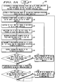
- FIGs. 3A and 3B are a logic flow diagram 300 of steps performed by test system 200 in tuning RF power amplifier 110 in accordance with an embodiment of the present invention.
- envelope tracking amplification system 100 is designed to operate over a range of supply voltages.
- Logic flow 300 begins (302) when test system 200 determines (304) a preferred operating point for envelope tracking amplification system 100 for each supply voltage of a first set of supply voltages, thereby producing multiple preferred operating points.
- a preferred operating point associated with each supply voltage of the first set of supply voltages may be predetermined by the designer of RF power amplifier 110 and stored in controller 208.
- a determination of a preferred operating point for each supply voltage of the first set of supply voltages may include the following steps.
- Variable voltage power supply 210 couples a first supply voltage of the first set of supply voltages to RF amplifying element 114 of RF power amplifier 110.
- signal generator 202 generates at least one test signal 203 that is coupled to input 109 of RF power amplifier 110.
- Test system controller 208 adjusts output matching circuit 116 in order to adjust an output impedance presented to RF amplifying element 114 and thereby an operating point of RF amplifying element 114.
- RF amplifying element 114 amplifies the at least one test signal based on the adjusted operating point to produce at least one amplified signal.
- Measurement device 204 measures an operating parameter, such as gain, phase, or IM, of RF power amplifier 110 based on the at least one amplified signal and the adjusted operating point.
- Test system controller 208 determines a preferred operating point associated with the first supply voltage by selecting an operating point corresponding to an optimal measured operating parameter.
- the preferred operating point is an operating point of RF amplifying element 114 that yields an optimal operating parameter.
- test system controller 208 adjusts an operating point of RF amplifying element 114 by adjusting the output impedance presented to the RF amplifying element. Controller 208 then determines an optimal operating point that corresponds to the optimal operating parameter as measured by measurement device 204.
- test system controller 208 determines a preferred operating point associated with the second supply voltage. The above process continues until a preferred operating point is determined for each supply voltage of the first set of supply voltages, thereby producing multiple preferred operating points.
- the at least one test signal may be set at multiple power levels, such as a swept power signal or signals, or may be set at a single power level, such as a lower end, a mid-range, or an upper end of a specified input signal power range of RF power amplifier 110.
- Test system controller 208 then optimizes an operating parameter of RF power amplifier 110 by adjusting output matching circuit 116 of the RF power amplifier in response to receipt of the test signal.
- the at least one test signal may comprise multiple test signals, wherein each test signal of the multiple test signals is at a same power level, but at a different frequency, than the other test signals of the multiple test signals.
- Test system controller 208 then optimizes an operating parameter of RF power amplifier 110 by adjusting output matching circuit 116 such that the operating parameter is optimized across each of the multiple test signal frequencies or such that the operating parameter attains a predetermined operating parameter threshold, which threshold is stored in the controller, at each of the multiple test signal frequencies.
- test system 200 Upon determining the multiple preferred operating points, test system 200, preferably test system controller 208, then sets (306) a first preferred operating point of the multiple preferred operating points for RF power amplifier 110, preferably by adjusting output matching circuit 116 of the RF power amplifier.
- test system 200 preferably variable voltage power supply 210, couples (308) to RF power amplifier 110 a first supply voltage of a second set of supply voltages.
- the second set of supply voltages may be the same as the first set of supply voltages. However, those who are of ordinary skill in the art realize that the second set of supply voltages may differ the first set of supply voltages without departing from the scope of the present invention.
- test system 200 preferably signal generator 202, couples (310) at least one test signal to input 109 of RF power amplifier 110, which at least one test signal may or may not be the same as the at least one test signal utilized to determine the multiple preferred operating points.
- RF power amplifier 110 Based on the coupled supply voltage of the second set of supply voltages, RF power amplifier 110 amplifies (312) the at least one test signal to produce at least one amplified signal.
- Test system 200 preferably measurement device 204 in conjunction with controller 208, then measures (314) an operating parameter of RF amplifier 110 based on the at least one amplified signal. For example, test system 200 may measure an output power of the at least one amplified signal, a gain or a phase shift of the at least one amplified signal relative to the corresponding test signal, or a distortion, such as IM, introduced to the at least one amplified signal by RF power amplifier 110.
- Test system 200 determines (316) a relationship between the at least one test signal, preferably a power associated with the at least one test signal, and the corresponding operating parameter measurements, and stores (318) information related to the determined relationship, such as data points or an algorithm describing a curve that defines the relationship.
- Test system 200 determines (320) whether each supply voltage of the second set of supply voltages has been coupled to RF power amplifier 110. When test system 200 determines that at least one supply voltage of the second set of supply voltages has not yet been coupled to RF power amplifier 110, test system 200, preferably variable voltage power supply 210, couples (322) one of the remaining, not yet coupled, supply voltages included in the second set of supply voltages to RF power amplifier 110 and repeats steps (310)-(320).
- test system 200 determines (324) an acceptable range of operation with respect to the set operating point.
- the determination of the acceptable range of operation is based on the relationship determined between the at least one test signal and the corresponding operating parameter measurements for each supply voltage of the second set of supply voltages.
- the acceptable range of operation describes the range of supply voltages over which RF power amplifier 110 is able to attain an acceptable operating parameter level.
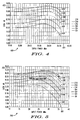
- FIGs. 4 and 5 depict an acceptable range of operation, that is, a range of supply voltages capable of providing a constant gain, for each of two different operating points of an RF power amplifier such as RF power amplifier 110.
- the RF power amplifier underlying each of FIGs. 4 and 5 includes an MRF187 power transistor, available from Motorola, Inc., of Schaumburg, Illinois, as the RF amplifying element included in the RF power amplifier.
- MRF187 is a 27 volt (V) part, that is, is rated for a maximum supply voltage of 27V.
- FIG. 4 graphs data produced by the RF power amplifier when tuned to a preferred operating point at the rated supply voltage of the RF amplifying element, that is, at 27V.
- FIG. 5 graphs data produced by the RF power amplifier when tuned to a preferred operating point at a lower supply voltage, that is, at 17V.
- FIG. 4 is a graphical representation 400 of a relationship between input signal power and gain for the RF power amplifier when tuned to a preferred operating point at 27V.
- a horizontal axis 401 of graph 400 depicts a power level (in dBm) of an input signal applied to the RF power amplifier, and a vertical axis 402 depicts a power gain (in decibels, or dB) of a signal output by the RF power amplifier in response to the application of the input signal.
- FIG. dBm power level of an input signal applied to the RF power amplifier
- a vertical axis 402 depicts a power gain (in decibels, or dB) of a signal output by the RF power amplifier in response to the application of the input signal.
- each curve 404-409 graphs a relationship between an input signal, that is, a power of the input signal, and an operating parameter, that is, a gain of the amplification system, for one of multiple supply voltages (six shown).
- the curves 404-409 respectively correspond to coupled supply voltages of 27 volts (V), 24V, 21V, 18V, 15V, and 12V.
- the variation in gain among the multiple supply voltage curves 404-409 is sufficiently dramatic that the RF power amplifier can maintain a constant gain (i.e., a constant gain trajectory) across only a very limited range of supply voltages. That is, the RF power amplifier depicted in FIG. 4 is able to achieve a constant gain, of approximately 14dB, only for supply voltages from 21 V to 27V. For supply voltages of less than 21 V, the RF power amplifier is unable to attain a gain of approximately 14dB regardless of the input power level, while for a supply voltage of 27V the RF power amplifier is unable to reduce its gain much below 14dB regardless of the input power level. Thus an acceptable range of operation for the RF power amplifier tuned at 27V is a supply voltage range of 21 V to 27V.
- FIG. 5 is a graphical representation 500 of a relationship between input signal power and gain for the RF power amplifier when tuned to a preferred operating point at 17V. Similar to FIG. 4 , a horizontal axis 501 of graph 500 depicts a power level (in dBm) of an input signal applied to the RF power amplifier, and a vertical axis 502 depicts a power gain (in dB) of a signal output by the RF power amplifier in response to the application of the input signal.
- FIG. 5 is a graphical representation 500 of a relationship between input signal power and gain for the RF power amplifier when tuned to a preferred operating point at 17V. Similar to FIG. 4 , a horizontal axis 501 of graph 500 depicts a power level (in dBm) of an input signal applied to the RF power amplifier, and a vertical axis 502 depicts a power gain (in dB) of a signal output by the RF power amplifier in response to the application of the input signal.
- each curve 504-510 graphs a relationship between an input signal, that is, a power of the input signal, and an operating parameter, that is, a gain of the RF power amplifier, for one of multiple supply voltages (seven shown).
- the curves 504-510 respectively correspond to applied supply voltages of 27 volts (V), 24V, 21V, 18V, 15V, 12V, and 9V.
- FIG. 5 depicts an RF power amplifier that is able to maintain a constant gain (i.e., a constant gain trajectory) across supply voltages ranging from 15V to 27V.
- a constant gain i.e., a constant gain trajectory
- test system 200 determines that each supply voltage of the second set of supply voltages has been coupled to RF power amplifier 110
- test system 200 preferably test system controller 208, further determines (326) whether each operating point of the multiple preferred operating points has been set for RF power amplifier 110.
- test system 200 determines that at least one operating point of the multiple preferred operating points has not been set for RF power amplifier 110
- test system 200 preferably controller 208, sets (328) one of the remaining, not yet set, operating points of the multiple preferred operating points for RF power amplifier 110.
- Test system 200 then repeats steps (308)-(326).
- test system 200 determines that each operating points of the multiple preferred operating points has been set for RF power amplifier 110
- test system 200 compares (330) the acceptable range of operation determined for each operating point of the multiple preferred operating points to the acceptable ranges of operation determined for the other operating points of the multiple preferred operating points to produce at least one comparison.
- Test system 200 preferably test system controller 208, then determines (332) an optimal operating point based on the at least one comparison. Based on the determined optimal operating point, test system 200, preferably test system controller 208, can determine (334) an optimal supply voltage for a tuning of RF power amplifier 110, which preferably is the supply voltage associated with the optimal operating point.
- Logic flow 300 then ends (336). The optimal operating point may then be implemented in RF power amplifier 110.
- FIG. 4 depicts an acceptable range of operation, that is, a range of supply voltages over which a constant gain can achieved (i.e., a constant gain trajectory), for an operating point that is set when an RF power amplifier is tuned at a supply voltage of 27V.
- the acceptable range of operation depicted by FIG. 4 is a supply voltage of 21V to 27V.
- FIG. 5 depicts an acceptable range of operation, that is, a supply voltage range of 15V to 27V, when the RF power amplifier is tuned at a supply voltage of 17V.
- tuning system 200 tunes RF power amplifier 110 at each of multiple supply voltages to determine a preferred operating point corresponding to each supply voltage. Tuning system 200 then determines an acceptable range of operation corresponding to each preferred operating point by setting RF power amplifier 110 at the preferred operating point and testing a performance of the RF power amplifier across a range of supply voltages. Tuning system 200 then compares the acceptable ranges of operation determined with respect the preferred operating points and determines an acceptable range of operation, and a corresponding preferred operating point, that yields the optimal performance. As a result, by tuning RF power amplifier 110 supply voltages that are less than a rated supply voltage of RF amplifying element 114, test system 200 is able to determine an optimal operating point with a broader range of acceptable operation than the prior art.
- RF power amplifier 110 may be tuned by test system 200 without determining a preferred operating point for each of multiple supply voltages.
- improvements in linearity of an RF power amplifier can be achieved by tuning the RF power amplifier, that is, by determining an optimal operating point based on adjustments of an output match of an RF amplifying element of the RF power amplifier, at a supply voltage that is significantly lower than the rated, or maximum, voltage of the RF amplifying element. Therefore, instead of determining a preferred operating point for each of multiple supply voltages, a tuning voltage that is less than the rated, or maximum, voltage of the RF amplifying element may be predetermined.
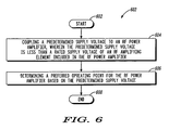
- FIG. 6 is a logic flow diagram 600 of a method for tuning RF power amplifier 110 without determining a preferred operating point for each of multiple supply voltages.
- Logic flow diagram 600 begins (602) when test system 200, preferably variable voltage supply 210, couples (604) a predetermined supply voltage to RF power amplifier 110. The predetermined supply voltage is less than a rated voltage of RF amplifying element 114. Test system 200 then determines (606) a preferred operating point for RF power amplifier 110 based on the predetermined supply voltage, and the logic flow ends (608).
- the step of determining (604) a preferred operating point includes the following steps.
- Test system 200 preferably signal generator 202, couples at least one test signal to RF power amplifier 110.
- Test system controller 208 adjusts output matching circuit 116 in order to adjust an output impedance presented to RF amplifying element 114 and thereby an operating point of the RF amplifying element 114.
- RF amplifying element 114 amplifies the at least one test signal based on the adjusted operating point to produce at least one amplified signal.
- Measurement device 204 measures an operating parameter, such as gain, phase, or IM, of RF power amplifier 110 based on the at least one amplified signal and the adjusted operating point.
- Test system controller 208 determines a preferred operating point associated with the predetermined supply voltage by selecting an operating point corresponding to an optimal measured operating parameter.
- the optimal tuning supply voltage has the same relationship to the rated, or maximum, voltage of the RF amplifying element as the average power of amplified signals produced by the RF power amplifier 110 has to the maximum linear output power, that is, to a power level corresponding to a 1dB gain compression point.
- the supply voltage used to tune up the RF power amplifier is approximately V rated /Sqrt(5), that is, the rated voltage divided by the square root of 5.
- V rated /Sqrt(5) the supply voltage used to tune the RF power amplifier for class B operation.
- an optimal tuning supply voltage for class AB operation is also less than the rated voltage of the RF amplifying element, as shown in FIGs.
- Optimal tuning supply voltages for other classes of operation can be determined and set by the designer of the RF power amplifier.
- test system 200 is able to determine an optimal operating point with a broader range of acceptable operation than the prior art.
- the implementation of the optimal operating point in envelope tracking amplification system 100 produces an amplification system of improved linearity over the amplification systems of the prior art.
Landscapes
- Engineering & Computer Science (AREA)
- Power Engineering (AREA)
- Amplifiers (AREA)
- Stabilization Of Oscillater, Synchronisation, Frequency Synthesizers (AREA)
- Input Circuits Of Receivers And Coupling Of Receivers And Audio Equipment (AREA)
- Paper (AREA)
- Variable-Direction Aerials And Aerial Arrays (AREA)
- Aerials With Secondary Devices (AREA)
Claims (12)
- Verfahren zum Abstimmen eines Hüllkurvenverfolgungsverstärkungssystems (100), das einen Radiofrequenz-(RF)-Leistungsverstärker (110) aufweist, wobei das Verfahren die folgenden Schritte umfasst:Bestimmen eines bevorzugten Betriebspunktes für den RF-Leistungsverstärker (110) für jede Versorgungsspannung einer ersten Reihe von Versorgungsspannungen zum Erhalt einer Vielzahl an bevorzugten Betriebspunkten;für jeden bevorzugten Betriebspunkt aus der Vielzahl an bevorzugten Betriebspunkten, Bestimmen, für jede Versorgungsspannung einer zweiten Reihe von Versorgungsspannungen, einer Beziehung zwischen einem Betriebsparameter des RF-Leistungsverstärkers (110) und einem Signal, das mit einem Eingang des RF-Leistungsverstärkers (110) gekoppelt ist, zum Erhalt einer Vielzahl an Beziehungen, die mit dem bevorzugten Betriebspunkt verknüpft sind;für jeden bevorzugten Betriebspunkt aus der Vielzahl an bevorzugten Betriebspunkten, Bestimmen eines Bereichs für den akzeptablen Betrieb des RF-Leistungsverstärkers (110) auf der Basis einer Vielzahl an Beziehungen, die mit dem bevorzugten Betriebspunkt verknüpft sind; undVergleichen des Bereichs des akzeptablen Betriebs, der in Bezug auf jeden bevorzugten Betriebspunkt aus der Vielzahl an bevorzugten Betriebspunkten bestimmt wird, mit den Bereichen des akzeptablen Betriebs, die in Bezug auf die anderen bevorzugten Betriebspunkte aus der Vielzahl an bevorzugten Betriebspunkten bestimmt werden, zum Erhalt von mindestens einem Vergleich; undBestimmen eines optimalen Betriebspunktes auf der Basis des mindestens einen Vergleichs.
- Verfahren nach Anspruch 1, weiterhin umfassend einen Schritt des Bestimmens einer optimalen Versorgungsspannung für ein Abstimmen des Radiofrequenz-Leistungsverstärkers (110) auf der Basis des bestimmten optimalen Betriebspunktes.
- Verfahren nach Anspruch 1, wobei der Schritt des Bestimmens eines bevorzugten Betriebspunktes für den Radiofrequenz-(RF)-Leistungsverstärker (110) für jede Versorgungsspannung einer ersten Reihe von Versorgungsspannungen die folgenden Schritte umfasst:Koppeln jeder Versorgungsspannung einer ersten Reihe von Versorgungsspannungen mit dem RF-Leistungsverstärker (110); und,als Antwort auf das Koppeln jeder Versorgungsspannung der ersten Reihe von Versorgungsspannungen mit dem RF-Leistungsverstärker (110), Bestimmen eines bevorzugten Betriebspunktes zum Erhalt einer Vielzahl an bevorzugten Betriebspunkten.
- Verfahren nach Anspruch 3, wobei der Radiofrequenz-(RF)-Leistungsverstärker (110) ein Radiofrequenzverstärkungselement umfasst, das mit einer Ausgangsabgleichschaltung gekoppelt ist, und wobei der Schritt des Bestimmens eines bevorzugten Betriebspunktes als Antwort auf das Koppeln jeder Versorgungsspannung der ersten Reihe von Versorgungsspannungen mit dem RF-Leistungsverstärker (110) einen Schritt des Anpassens der Ausgangsabgleichschaltung zum Erhalt eines bevorzugten Betriebspunktes für den RF-Leistungsverstärker (110) umfasst.
- Verfahren nach Anspruch 3, wobei der Schritt des Bestimmens eines bevorzugten Betriebspunktes für jede Versorgungsspannung einer ersten Reihe von Versorgungsspannungen zum Erhalt einer Vielzahl an bevorzugten Betriebspunkten die folgenden Schritte umfasst:für jede Versorgungsspannung einer ersten Reihe von Versorgungsspannungen:Koppeln der Versorgungsspannung mit dem Radiofrequenz-(RF)-Leistungsverstärker (110);Koppeln von mindestens einem Testsignal mit dem RF-Leistungsverstärker (110);Verstärken des mindestens einen Testsignals zum Erhalt von mindestens einem verstärkten Signal; undBestimmen eines bevorzugten Betriebspunktes für die Versorgungsspannung auf der Basis des mindestens einen verstärkten Signals.
- Verfahren nach Anspruch 5, wobei der Betriebsparameter eine Verstärkung des Radiofrequenz-(RF)-Leistungsverstärkers (110) umfasst und wobei der Schritt des Bestimmens eines Bereichs für den akzeptablen Betrieb des RF-Leistungsverstärkers (110) für jeden bevorzugten Betriebspunkt aus der Vielzahl an bevorzugten Betriebspunkten einen Schritt des Bestimmens einer stetigen Verstärkungskurve für jeden bevorzugten Betriebspunkt aus der Vielzahl an bevorzugten Betriebspunkten umfasst.
- Verfahren nach Anspruch 1, wobei der Schritt des Bestimmens einer Beziehung zwischen einem Betriebsparameter des Radiofrequenz-(RF)-Leistungsverstärkers (110) und eines Signals, das mit einem Eingang des RF-Leistungsverstärkers (110) für jede Versorgungsspannung einer zweiten Reihe von Versorgungsspannungen gekoppelt ist, die folgenden Schritte umfasst:für jede Versorgungsspannung einer zweiten Reihe von Versorgungsspannungen:Ermitteln eines bevorzugten Betriebspunktes des RF-Leistungsverstärkers (110);Koppeln der Versorgungsspannung mit dem Radiofrequenz-(RF)-Leistungsverstärker (110);Koppeln einer Vielzahl an Testsignalen mit dem RF-Leistungsverstärker (110);Hervorbringen einer Vielzahl an verstärkten Signalen auf der Basis der Vielzahl an Testsignalen, wobei jedes verstärkte Signal aus der Vielzahl an verstärkten Signalen einem Testsignal aus der Vielzahl an Testsignalen entspricht;Bestimmen, in Bezug auf jedes Testsignal und das entsprechende verstärkte Signal, eines Betriebsparameters des RF-Leistungsverstärkers (110) zum Erhalt einer Vielzahl an Betriebsparametern; undBestimmen einer Beziehung zwischen der Vielzahl an Testsignalen und der Vielzahl an Betriebsparametern.
- Verfahren nach Anspruch 1, wobei für jeden bevorzugten Betriebspunkt aus der Vielzahl an bevorzugten Betriebspunkten, für jede Versorgungsspannung einer zweiten Reihe von Versorgungsspannungen, das Bestimmen einer Beziehung zwischen einem Betriebsparameter des RF-Leistungsverstärkers (110) und einem Signal, das mit einem Eingang des RF-Leistungsverstärkers (110) gekoppelt ist, zum Erhalt einer Vielzahl an Beziehungen, die mit dem bevorzugten Betriebspunkt verknüpft sind, die folgenden Schritte umfasst:Festsetzen eines ersten Betriebspunktes aus der Vielzahl an Betriebspunkten und als Antwort auf das Festsetzen des ersten Betriebspunktes:Koppeln einer ersten Versorgungsspannung der zweiten Reihe von Versorgungsspannungen mit dem RF-Leistungsverstärker (110);Koppeln eines ersten Eingangssignals mit einem Eingang des RF-Leistungsverstärkers (110);Verstärken des ersten Eingangssignals zum Erhalt eines ersten verstärkten Signals;Messen eines Betriebsparameters des RF-Leistungsverstärkers (110) auf der Basis des ersten verstärkten Signals zum Erhalt einer ersten Betriebsparametermessung;Koppeln einer zweiten Versorgungsspannung einer zweiten Reihe von Versorgungsspannungen mit dem RF-Leistungsverstärker (110);Koppeln eines zweiten Eingangssignals mit dem Eingang des RF-Leistungsverstärkers (110);Verstärken des zweiten Eingangssignals zum Erhalt eines zweiten verstärkten Signals;Messen eines Betriebsparameters des RF-Leistungsverstärkers (110) auf der Basis des Eingangssignals und des zweiten verstärkten Signals zum Erhalt einer zweiten Betriebsparametermessung;Festsetzen eines zweiten Betriebspunktes aus der Vielzahl an Betriebspunkte und als Antwort auf das Festsetzen des zweiten Betriebspunktes:wobei das Bestimmen eines optimalen Betriebspunktes das Bestimmen eines optimalen Betriebspunktes auf der Basis der ersten Betriebsparametermessung, der zweiten Betriebsparametermessung, der dritten Betriebsparametermessung und der vierten Betriebsparametermessung umfasst.Koppeln der ersten Versorgungsspannung der zweiten Reihe von Versorgungsspannungen mit dem RF-Leistungsverstärker (110);Koppeln eines dritten Eingangssignals mit dem Eingang des RF-Leistungsverstärkers (110);Verstärken des dritten Eingangssignals zum Erhalt eines dritten verstärkten Signals;Messen eines Betriebsparameters des RF-Leistungsverstärkers (110) auf der Basis des dritten verstärkten Signals zum Erhalt einer dritten Betriebsparametermessung;Koppeln der zweiten Versorgungsspannung der zweiten Reihe von Versorgungsspannungen mit dem RF-Leistungsverstärker (110);Koppeln eines vierten Eingangssignals mit einem Eingang des RF-Leistungsverstärkers (110);Verstärken des vierten Eingangssignals zum Erhalt eines vierten verstärkten Signals;Messen eines Betriebsparameters des RF-Leistungsverstärkers (110) auf der Basis des vierten verstärkten Signals zum Erhalt einer vierten Betriebsparametermessung; und
- Verfahren nach Anspruch 8, weiterhin umfassend einen Schritt des Bestimmens einer optimalen Versorgungsspannung für ein Abstimmen des Radiofrequenz-Leistungsverstärkers (110) auf der Basis des bestimmten optimalen Betriebspunktes.
- Verfahren nach Anspruch 8, wobei jeder der gemessenen Betriebsparameter mindestens eines von Folgendem umfasst: eine Verstärkung des Radiofrequenz-Leistungsverstärkers (110), eine Verzerrung, die dem jeweiligen verstärkten Signal durch den Radiofrequenz-Leistungsverstärker (110) zugefügt wurde, oder eine mit dem Radiofrequenz-Leistungsverstärker (110) verknüpfte Phasenverschiebung.
- Verfahren zum Abstimmen eines Hüllkurvenverfolgungsverstärkungssystems, umfassend einen Radiofrequenz-(RF)-Leistungsverstärker mit einem RF-Verstärkungselement, wobei das Verfahren die folgenden Schritte umfasst:Koppeln einer vorbestimmten Versorgungsspannung mit dem RF-Leistungsverstärker (110), wobei die vorbestimmte Versorgungsspannung weniger als eine Nennspannung des RF-Verstärkungselements beträgt; undBestimmen eines bevorzugten Betriebspunktes für den RF-Leistungsverstärker auf der Basis der vorbestimmten Versorgungsspannung.
- Verfahren nach Anspruch 11, wobei das Radiofrequenz-(RF-) Verstärkungselement mit einer anpassungsfähigen Ausgangsabgleichschaltung gekoppelt ist und wobei der Schritt des Bestimmens eines bevorzugten Betriebspunktes die folgenden Schritte umfasst:Koppeln von mindestens einem Testsignal mit dem RF-Leistungsverstärker;als Antwort auf das Koppeln des mindestens einen Testsignals mit dem RF-Leistungsverstärker, Anpassen der Ausgangsabgleichschaltung, um einen festgelegten Betriebsparameter des RF-Leistungsverstärkers zu optimieren; undBestimmen eines bevorzugten Betriebspunktes auf der Basis der Optimierung des festgelegten Betriebsparameters.
Applications Claiming Priority (3)
| Application Number | Priority Date | Filing Date | Title |
|---|---|---|---|
| US10/175,666 US6725021B1 (en) | 2002-06-20 | 2002-06-20 | Method for tuning an envelope tracking amplification system |
| US175666 | 2002-06-20 | ||
| PCT/US2003/013902 WO2004002006A1 (en) | 2002-06-20 | 2003-05-05 | Method for tuning an envelope tracking amplification system |
Publications (3)
| Publication Number | Publication Date |
|---|---|
| EP1518335A1 EP1518335A1 (de) | 2005-03-30 |
| EP1518335A4 EP1518335A4 (de) | 2005-08-17 |
| EP1518335B1 true EP1518335B1 (de) | 2009-07-01 |
Family
ID=29999048
Family Applications (1)
| Application Number | Title | Priority Date | Filing Date |
|---|---|---|---|
| EP03761021A Expired - Lifetime EP1518335B1 (de) | 2002-06-20 | 2003-05-05 | Verfahren zum abstimmen eines hüllkurvenverfolgungs-verstärkungssystems |
Country Status (8)
| Country | Link |
|---|---|
| US (1) | US6725021B1 (de) |
| EP (1) | EP1518335B1 (de) |
| AT (1) | ATE435532T1 (de) |
| AU (1) | AU2003243194A1 (de) |
| CA (1) | CA2489796A1 (de) |
| DE (1) | DE60328190D1 (de) |
| IL (1) | IL165799A0 (de) |
| WO (1) | WO2004002006A1 (de) |
Families Citing this family (98)
| Publication number | Priority date | Publication date | Assignee | Title |
|---|---|---|---|---|
| AU2002367231A1 (en) * | 2001-12-24 | 2003-07-15 | Koninklijke Philips Electronics N.V. | Power amplifier |
| US7079818B2 (en) * | 2002-02-12 | 2006-07-18 | Broadcom Corporation | Programmable mutlistage amplifier and radio applications thereof |
| FI115935B (fi) * | 2003-02-25 | 2005-08-15 | Nokia Corp | Menetelmä ja laite tehovahvistimen ominaisuuksien säätämiseksi |
| WO2007016965A1 (en) * | 2005-08-09 | 2007-02-15 | Freescale Semiconductor, Inc | Wireless communication unit, integrated circuit and method for biasing a power amplifier |
| JP4868846B2 (ja) * | 2005-12-22 | 2012-02-01 | 富士通株式会社 | 電圧制御信号調整装置及び電圧制御信号調整方法 |
| US7519336B2 (en) * | 2006-05-05 | 2009-04-14 | Nokia Corporation | Method and arrangement for optimizing efficiency of a power amplifier |
| US7570931B2 (en) * | 2006-06-02 | 2009-08-04 | Crestcom, Inc. | RF transmitter with variably biased RF power amplifier and method therefor |
| US7620377B2 (en) * | 2006-08-30 | 2009-11-17 | General Dynamics C4 Systems | Bandwidth enhancement for envelope elimination and restoration transmission systems |
| WO2008032264A2 (en) * | 2006-09-12 | 2008-03-20 | Nxp B.V. | Amplifier architecture for polar modulation |
| US7729670B2 (en) * | 2006-09-29 | 2010-06-01 | Broadcom Corporation | Method and system for minimizing power consumption in a communication system |
| US8064851B2 (en) * | 2008-03-06 | 2011-11-22 | Crestcom, Inc. | RF transmitter with bias-signal-induced distortion compensation and method therefor |
| US8320850B1 (en) * | 2009-03-18 | 2012-11-27 | Rf Micro Devices, Inc. | Power control loop using a tunable antenna matching circuit |
| WO2011002171A2 (ko) * | 2009-07-02 | 2011-01-06 | 삼성전자 주식회사 | 휴대 단말기 안테나의 정합 방법 및 이를 위한 장치 |
| US9112452B1 (en) | 2009-07-14 | 2015-08-18 | Rf Micro Devices, Inc. | High-efficiency power supply for a modulated load |
| US20110217926A1 (en) * | 2010-03-03 | 2011-09-08 | Qualcomm Incorporated | Reverse link signaling via impedance modulation |
| GB2479859B (en) * | 2010-03-30 | 2017-08-30 | Snaptrack Inc | Signal alignment for envelope tracking system |
| US8583062B2 (en) | 2010-04-15 | 2013-11-12 | Apple Inc. | Methods for determining optimum power supply voltages for radio-frequency power amplifier circuitry |
| US9431974B2 (en) | 2010-04-19 | 2016-08-30 | Qorvo Us, Inc. | Pseudo-envelope following feedback delay compensation |
| WO2011133542A1 (en) | 2010-04-19 | 2011-10-27 | Rf Micro Devices, Inc. | Pseudo-envelope following power management system |
| US8519788B2 (en) | 2010-04-19 | 2013-08-27 | Rf Micro Devices, Inc. | Boost charge-pump with fractional ratio and offset loop for supply modulation |
| US8633766B2 (en) | 2010-04-19 | 2014-01-21 | Rf Micro Devices, Inc. | Pseudo-envelope follower power management system with high frequency ripple current compensation |
| US9099961B2 (en) | 2010-04-19 | 2015-08-04 | Rf Micro Devices, Inc. | Output impedance compensation of a pseudo-envelope follower power management system |
| US8981848B2 (en) | 2010-04-19 | 2015-03-17 | Rf Micro Devices, Inc. | Programmable delay circuitry |
| US8866549B2 (en) | 2010-06-01 | 2014-10-21 | Rf Micro Devices, Inc. | Method of power amplifier calibration |
| CN102340283B (zh) * | 2010-07-14 | 2014-05-28 | 大唐移动通信设备有限公司 | 一种包络跟踪的方法及装置 |
| WO2012027039A1 (en) | 2010-08-25 | 2012-03-01 | Rf Micro Devices, Inc. | Multi-mode/multi-band power management system |
| US9954436B2 (en) | 2010-09-29 | 2018-04-24 | Qorvo Us, Inc. | Single μC-buckboost converter with multiple regulated supply outputs |
| US8782107B2 (en) | 2010-11-16 | 2014-07-15 | Rf Micro Devices, Inc. | Digital fast CORDIC for envelope tracking generation |
| US8588713B2 (en) | 2011-01-10 | 2013-11-19 | Rf Micro Devices, Inc. | Power management system for multi-carriers transmitter |
| WO2012106437A1 (en) * | 2011-02-02 | 2012-08-09 | Rf Micro Devices, Inc. | Fast envelope system calibration |
| US8624760B2 (en) | 2011-02-07 | 2014-01-07 | Rf Micro Devices, Inc. | Apparatuses and methods for rate conversion and fractional delay calculation using a coefficient look up table |
| JP5996559B2 (ja) * | 2011-02-07 | 2016-09-21 | スカイワークス ソリューションズ, インコーポレイテッドSkyworks Solutions, Inc. | 包絡線トラッキング較正のための装置および方法 |
| CN103444076B (zh) | 2011-02-07 | 2016-05-04 | 射频小型装置公司 | 用于功率放大器包络跟踪的群延迟校准方法 |
| DE102011012927B4 (de) * | 2011-03-03 | 2020-01-02 | Snaptrack, Inc. | Verstärkermodul |
| US9247496B2 (en) | 2011-05-05 | 2016-01-26 | Rf Micro Devices, Inc. | Power loop control based envelope tracking |
| US9379667B2 (en) | 2011-05-05 | 2016-06-28 | Rf Micro Devices, Inc. | Multiple power supply input parallel amplifier based envelope tracking |
| US9246460B2 (en) | 2011-05-05 | 2016-01-26 | Rf Micro Devices, Inc. | Power management architecture for modulated and constant supply operation |
| CN103748794B (zh) | 2011-05-31 | 2015-09-16 | 射频小型装置公司 | 一种用于测量发射路径的复数增益的方法和设备 |
| US9019011B2 (en) | 2011-06-01 | 2015-04-28 | Rf Micro Devices, Inc. | Method of power amplifier calibration for an envelope tracking system |
| US8760228B2 (en) | 2011-06-24 | 2014-06-24 | Rf Micro Devices, Inc. | Differential power management and power amplifier architecture |
| WO2013012787A2 (en) | 2011-07-15 | 2013-01-24 | Rf Micro Devices, Inc. | Modified switching ripple for envelope tracking system |
| US8626091B2 (en) | 2011-07-15 | 2014-01-07 | Rf Micro Devices, Inc. | Envelope tracking with variable compression |
| US8952710B2 (en) | 2011-07-15 | 2015-02-10 | Rf Micro Devices, Inc. | Pulsed behavior modeling with steady state average conditions |
| US9263996B2 (en) | 2011-07-20 | 2016-02-16 | Rf Micro Devices, Inc. | Quasi iso-gain supply voltage function for envelope tracking systems |
| US8761698B2 (en) | 2011-07-27 | 2014-06-24 | Intel Mobile Communications GmbH | Transmit circuit, method for adjusting a bias of a power amplifier and method for adapting the provision of a bias information |
| US8618868B2 (en) | 2011-08-17 | 2013-12-31 | Rf Micro Devices, Inc. | Single charge-pump buck-boost for providing independent voltages |
| US8942652B2 (en) | 2011-09-02 | 2015-01-27 | Rf Micro Devices, Inc. | Split VCC and common VCC power management architecture for envelope tracking |
| US8957728B2 (en) | 2011-10-06 | 2015-02-17 | Rf Micro Devices, Inc. | Combined filter and transconductance amplifier |
| US9484797B2 (en) | 2011-10-26 | 2016-11-01 | Qorvo Us, Inc. | RF switching converter with ripple correction |
| CN103988406B (zh) | 2011-10-26 | 2017-03-01 | Qorvo美国公司 | 射频(rf)开关转换器以及使用rf开关转换器的rf放大装置 |
| US9024688B2 (en) | 2011-10-26 | 2015-05-05 | Rf Micro Devices, Inc. | Dual parallel amplifier based DC-DC converter |
| CN103959189B (zh) | 2011-10-26 | 2015-12-23 | 射频小型装置公司 | 基于电感的并行放大器相位补偿 |
| US8975959B2 (en) | 2011-11-30 | 2015-03-10 | Rf Micro Devices, Inc. | Monotonic conversion of RF power amplifier calibration data |
| US9515621B2 (en) | 2011-11-30 | 2016-12-06 | Qorvo Us, Inc. | Multimode RF amplifier system |
| US9250643B2 (en) | 2011-11-30 | 2016-02-02 | Rf Micro Devices, Inc. | Using a switching signal delay to reduce noise from a switching power supply |
| US9256234B2 (en) | 2011-12-01 | 2016-02-09 | Rf Micro Devices, Inc. | Voltage offset loop for a switching controller |
| US9041365B2 (en) | 2011-12-01 | 2015-05-26 | Rf Micro Devices, Inc. | Multiple mode RF power converter |
| US9041364B2 (en) | 2011-12-01 | 2015-05-26 | Rf Micro Devices, Inc. | RF power converter |
| US8947161B2 (en) | 2011-12-01 | 2015-02-03 | Rf Micro Devices, Inc. | Linear amplifier power supply modulation for envelope tracking |
| US9494962B2 (en) | 2011-12-02 | 2016-11-15 | Rf Micro Devices, Inc. | Phase reconfigurable switching power supply |
| US9813036B2 (en) | 2011-12-16 | 2017-11-07 | Qorvo Us, Inc. | Dynamic loadline power amplifier with baseband linearization |
| US9298198B2 (en) | 2011-12-28 | 2016-03-29 | Rf Micro Devices, Inc. | Noise reduction for envelope tracking |
| GB2500709A (en) * | 2012-03-30 | 2013-10-02 | Nujira Ltd | Characterisation of an envelope-tracking amplifier by use of a set of envelope shaping functions |
| US8981839B2 (en) | 2012-06-11 | 2015-03-17 | Rf Micro Devices, Inc. | Power source multiplexer |
| US9020451B2 (en) | 2012-07-26 | 2015-04-28 | Rf Micro Devices, Inc. | Programmable RF notch filter for envelope tracking |
| US9225231B2 (en) | 2012-09-14 | 2015-12-29 | Rf Micro Devices, Inc. | Open loop ripple cancellation circuit in a DC-DC converter |
| US9197256B2 (en) | 2012-10-08 | 2015-11-24 | Rf Micro Devices, Inc. | Reducing effects of RF mixer-based artifact using pre-distortion of an envelope power supply signal |
| WO2014062902A1 (en) | 2012-10-18 | 2014-04-24 | Rf Micro Devices, Inc | Transitioning from envelope tracking to average power tracking |
| US9627975B2 (en) | 2012-11-16 | 2017-04-18 | Qorvo Us, Inc. | Modulated power supply system and method with automatic transition between buck and boost modes |
| US10243519B2 (en) | 2012-12-28 | 2019-03-26 | Psemi Corporation | Bias control for stacked transistor configuration |
| US9680434B2 (en) * | 2012-12-28 | 2017-06-13 | Mediatek, Inc. | Method and apparatus for calibrating an envelope tracking system |
| US11128261B2 (en) | 2012-12-28 | 2021-09-21 | Psemi Corporation | Constant Vds1 bias control for stacked transistor configuration |
| US9219445B2 (en) | 2012-12-28 | 2015-12-22 | Peregrine Semiconductor Corporation | Optimization methods for amplifier with variable supply power |
| US9716477B2 (en) | 2012-12-28 | 2017-07-25 | Peregrine Semiconductor Corporation | Bias control for stacked transistor configuration |
| WO2014116933A2 (en) | 2013-01-24 | 2014-07-31 | Rf Micro Devices, Inc | Communications based adjustments of an envelope tracking power supply |
| US8824981B2 (en) * | 2013-01-31 | 2014-09-02 | Intel Mobile Communications GmbH | Recalibration of envelope tracking transfer function during active transmission |
| US9178472B2 (en) | 2013-02-08 | 2015-11-03 | Rf Micro Devices, Inc. | Bi-directional power supply signal based linear amplifier |
| US9203353B2 (en) | 2013-03-14 | 2015-12-01 | Rf Micro Devices, Inc. | Noise conversion gain limited RF power amplifier |
| WO2014152903A2 (en) | 2013-03-14 | 2014-09-25 | Rf Micro Devices, Inc | Envelope tracking power supply voltage dynamic range reduction |
| US9479118B2 (en) | 2013-04-16 | 2016-10-25 | Rf Micro Devices, Inc. | Dual instantaneous envelope tracking |
| KR101738730B1 (ko) | 2013-04-23 | 2017-05-22 | 스카이워크스 솔루션즈, 인코포레이티드 | 전력 증폭기 시스템에서의 엔벨로프 정형화 장치 및 방법 |
| US8909180B1 (en) | 2013-06-26 | 2014-12-09 | Motorola Solutions, Inc. | Method and apparatus for power supply modulation of a radio frequency signal |
| US9166830B2 (en) | 2013-07-18 | 2015-10-20 | Intel Deutschland Gmbh | Systems and methods utilizing adaptive envelope tracking |
| US9374005B2 (en) | 2013-08-13 | 2016-06-21 | Rf Micro Devices, Inc. | Expanded range DC-DC converter |
| US9882536B2 (en) * | 2013-09-18 | 2018-01-30 | Hitachi Kokusai Electric Inc. | Wireless apparatus and method for controlling voltage supplied to amplifier unit |
| US20150236877A1 (en) * | 2014-02-14 | 2015-08-20 | Mediatek Inc. | Methods and apparatus for envelope tracking system |
| US9520907B2 (en) | 2014-02-16 | 2016-12-13 | Mediatek Inc. | Methods and apparatus for envelope tracking system |
| US9614476B2 (en) | 2014-07-01 | 2017-04-04 | Qorvo Us, Inc. | Group delay calibration of RF envelope tracking |
| DE102015110238A1 (de) | 2015-06-25 | 2016-12-29 | Intel IP Corporation | Eine Schaltung und ein Verfahren zum Erzeugen eines Radiofrequenzsignals |
| US20170005624A1 (en) | 2015-06-30 | 2017-01-05 | Skyworks Solutions, Inc. | Parallel amplifier linearization in a radio frequency system |
| US9912297B2 (en) | 2015-07-01 | 2018-03-06 | Qorvo Us, Inc. | Envelope tracking power converter circuitry |
| US9948240B2 (en) | 2015-07-01 | 2018-04-17 | Qorvo Us, Inc. | Dual-output asynchronous power converter circuitry |
| US9973147B2 (en) | 2016-05-10 | 2018-05-15 | Qorvo Us, Inc. | Envelope tracking power management circuit |
| US9837965B1 (en) | 2016-09-16 | 2017-12-05 | Peregrine Semiconductor Corporation | Standby voltage condition for fast RF amplifier bias recovery |
| US9960737B1 (en) | 2017-03-06 | 2018-05-01 | Psemi Corporation | Stacked PA power control |
| US10276371B2 (en) | 2017-05-19 | 2019-04-30 | Psemi Corporation | Managed substrate effects for stabilized SOI FETs |
| US10476437B2 (en) | 2018-03-15 | 2019-11-12 | Qorvo Us, Inc. | Multimode voltage tracker circuit |
| US12206363B2 (en) * | 2021-05-26 | 2025-01-21 | Skyworks Solutions, Inc. | Load modulated power amplifiers |
Family Cites Families (13)
| Publication number | Priority date | Publication date | Assignee | Title |
|---|---|---|---|---|
| US5251331A (en) | 1992-03-13 | 1993-10-05 | Motorola, Inc. | High efficiency dual mode power amplifier apparatus |
| US5420536A (en) * | 1993-03-16 | 1995-05-30 | Victoria University Of Technology | Linearized power amplifier |
| KR970007602B1 (ko) * | 1994-05-31 | 1997-05-13 | 삼성전자 주식회사 | 전송기의 출력전력을 제어 및 측정하기 위한 장치 및 그에 따른 방법 |
| US6163706A (en) * | 1997-11-18 | 2000-12-19 | Conexant Systems, Inc. | Apparatus for and method of improving efficiency of transceivers in radio products |
| US6138042A (en) * | 1997-12-31 | 2000-10-24 | Motorola, Inc. | Method, device, phone, and base station for providing an efficient tracking power converter for variable signals |
| US6141541A (en) * | 1997-12-31 | 2000-10-31 | Motorola, Inc. | Method, device, phone and base station for providing envelope-following for variable envelope radio frequency signals |
| US6064269A (en) * | 1998-07-31 | 2000-05-16 | Motorola, Inc. | Power amplifier with variable input voltage source |
| US6043707A (en) * | 1999-01-07 | 2000-03-28 | Motorola, Inc. | Method and apparatus for operating a radio-frequency power amplifier as a variable-class linear amplifier |
| US5977759A (en) | 1999-02-25 | 1999-11-02 | Nortel Networks Corporation | Current mirror circuits for variable supply voltages |
| US6349216B1 (en) * | 1999-07-22 | 2002-02-19 | Motorola, Inc. | Load envelope following amplifier system |
| US6449465B1 (en) * | 1999-12-20 | 2002-09-10 | Motorola, Inc. | Method and apparatus for linear amplification of a radio frequency signal |
| GB0028689D0 (en) * | 2000-11-24 | 2001-01-10 | Qualcomm Uk Ltd | Amplifier circuit |
| US6348781B1 (en) | 2000-12-11 | 2002-02-19 | Motorola, Inc. | Buck or boost power converter |
-
2002
- 2002-06-20 US US10/175,666 patent/US6725021B1/en not_active Expired - Lifetime
-
2003
- 2003-05-05 DE DE60328190T patent/DE60328190D1/de not_active Expired - Fee Related
- 2003-05-05 AU AU2003243194A patent/AU2003243194A1/en not_active Abandoned
- 2003-05-05 CA CA002489796A patent/CA2489796A1/en not_active Abandoned
- 2003-05-05 EP EP03761021A patent/EP1518335B1/de not_active Expired - Lifetime
- 2003-05-05 AT AT03761021T patent/ATE435532T1/de not_active IP Right Cessation
- 2003-05-05 WO PCT/US2003/013902 patent/WO2004002006A1/en not_active Ceased
-
2004
- 2004-12-16 IL IL16579904A patent/IL165799A0/xx unknown
Also Published As
| Publication number | Publication date |
|---|---|
| WO2004002006A1 (en) | 2003-12-31 |
| EP1518335A1 (de) | 2005-03-30 |
| DE60328190D1 (de) | 2009-08-13 |
| AU2003243194A1 (en) | 2004-01-06 |
| IL165799A0 (en) | 2006-01-15 |
| CA2489796A1 (en) | 2003-12-31 |
| EP1518335A4 (de) | 2005-08-17 |
| ATE435532T1 (de) | 2009-07-15 |
| US6725021B1 (en) | 2004-04-20 |
Similar Documents
| Publication | Publication Date | Title |
|---|---|---|
| EP1518335B1 (de) | Verfahren zum abstimmen eines hüllkurvenverfolgungs-verstärkungssystems | |
| US6735419B2 (en) | High efficiency wideband linear wireless power amplifier | |
| US5915213A (en) | Transmitter apparatus with linearizing circuit to compensate for distortion in power amplifier | |
| US6160449A (en) | Power amplifying circuit with load adjust for control of adjacent and alternate channel power | |
| US5625322A (en) | Amplifier bias control device | |
| KR100372857B1 (ko) | 인접 채널 및 대체 채널 전력을 제어하기 위해 공급 조정을 갖는 전력 증폭 회로 | |
| US7444125B2 (en) | Communications signal amplifiers having independent power control and amplitude modulation | |
| US6677820B2 (en) | Distortion compensation apparatus | |
| US20050287965A1 (en) | Low current direct conversion transmitter architecture | |
| US20110269416A1 (en) | Transmitter | |
| US6696866B2 (en) | Method and apparatus for providing a supply voltage based on an envelope of a radio frequency signal | |
| US20140210558A1 (en) | Systems and methods for biasing amplifiers using adaptive closed-loop control and adaptive predistortion | |
| US20080261543A1 (en) | Transmission circuit and communication device | |
| US8270916B2 (en) | Methods for tuning and controlling output power in polar transmitters | |
| US20090011730A1 (en) | Methods and Apparatus for Controlling Power in a Polar Modulation Transmitter | |
| US5373251A (en) | Transmission output amplifier | |
| JP3396643B2 (ja) | 増幅器線形化装置の適応制御方法 | |
| JP4286455B2 (ja) | 利得制御回路およびパイロット信号を用いる可変増幅器の利得制御を与える方法 | |
| EP2091144B1 (de) | Übertragungsverfahren und übertragungseinrichtung | |
| JP2004527140A (ja) | 第2の集積回路の信号利得に基づく第1の集積回路におけるバイアス電流の調整 | |
| EP1601096A1 (de) | Verfahren und elektronische Schleifenschaltung zur Einstellung der Vorspannung | |
| MXPA00007176A (en) | Power amplifying circuit with load adjust for control of adjacent and alternate channel power |
Legal Events
| Date | Code | Title | Description |
|---|---|---|---|
| PUAI | Public reference made under article 153(3) epc to a published international application that has entered the european phase |
Free format text: ORIGINAL CODE: 0009012 |
|
| 17P | Request for examination filed |
Effective date: 20050120 |
|
| AK | Designated contracting states |
Kind code of ref document: A1 Designated state(s): AT BE BG CH CY CZ DE DK EE ES FI FR GB GR HU IE IT LI LU MC NL PT RO SE SI SK TR |
|
| AX | Request for extension of the european patent |
Extension state: AL LT LV MK |
|
| A4 | Supplementary search report drawn up and despatched |
Effective date: 20050705 |
|
| RIC1 | Information provided on ipc code assigned before grant |
Ipc: 7H 03F 1/02 B Ipc: 7H 03G 3/30 B Ipc: 7H 03G 3/00 B Ipc: 7H 04B 7/00 A |
|
| DAX | Request for extension of the european patent (deleted) | ||
| GRAP | Despatch of communication of intention to grant a patent |
Free format text: ORIGINAL CODE: EPIDOSNIGR1 |
|
| GRAS | Grant fee paid |
Free format text: ORIGINAL CODE: EPIDOSNIGR3 |
|
| GRAA | (expected) grant |
Free format text: ORIGINAL CODE: 0009210 |
|
| AK | Designated contracting states |
Kind code of ref document: B1 Designated state(s): AT BE BG CH CY CZ DE DK EE ES FI FR GB GR HU IE IT LI LU MC NL PT RO SE SI SK TR |
|
| REG | Reference to a national code |
Ref country code: GB Ref legal event code: FG4D |
|
| REG | Reference to a national code |
Ref country code: CH Ref legal event code: EP |
|
| REG | Reference to a national code |
Ref country code: IE Ref legal event code: FG4D |
|
| REF | Corresponds to: |
Ref document number: 60328190 Country of ref document: DE Date of ref document: 20090813 Kind code of ref document: P |
|
| PG25 | Lapsed in a contracting state [announced via postgrant information from national office to epo] |
Ref country code: SI Free format text: LAPSE BECAUSE OF FAILURE TO SUBMIT A TRANSLATION OF THE DESCRIPTION OR TO PAY THE FEE WITHIN THE PRESCRIBED TIME-LIMIT Effective date: 20090701 |
|
| NLV1 | Nl: lapsed or annulled due to failure to fulfill the requirements of art. 29p and 29m of the patents act | ||
| PG25 | Lapsed in a contracting state [announced via postgrant information from national office to epo] |
Ref country code: FI Free format text: LAPSE BECAUSE OF FAILURE TO SUBMIT A TRANSLATION OF THE DESCRIPTION OR TO PAY THE FEE WITHIN THE PRESCRIBED TIME-LIMIT Effective date: 20090701 Ref country code: SE Free format text: LAPSE BECAUSE OF FAILURE TO SUBMIT A TRANSLATION OF THE DESCRIPTION OR TO PAY THE FEE WITHIN THE PRESCRIBED TIME-LIMIT Effective date: 20090701 Ref country code: AT Free format text: LAPSE BECAUSE OF FAILURE TO SUBMIT A TRANSLATION OF THE DESCRIPTION OR TO PAY THE FEE WITHIN THE PRESCRIBED TIME-LIMIT Effective date: 20090701 Ref country code: EE Free format text: LAPSE BECAUSE OF FAILURE TO SUBMIT A TRANSLATION OF THE DESCRIPTION OR TO PAY THE FEE WITHIN THE PRESCRIBED TIME-LIMIT Effective date: 20090701 Ref country code: ES Free format text: LAPSE BECAUSE OF FAILURE TO SUBMIT A TRANSLATION OF THE DESCRIPTION OR TO PAY THE FEE WITHIN THE PRESCRIBED TIME-LIMIT Effective date: 20091012 |
|
| PG25 | Lapsed in a contracting state [announced via postgrant information from national office to epo] |
Ref country code: NL Free format text: LAPSE BECAUSE OF FAILURE TO SUBMIT A TRANSLATION OF THE DESCRIPTION OR TO PAY THE FEE WITHIN THE PRESCRIBED TIME-LIMIT Effective date: 20090701 |
|
| PG25 | Lapsed in a contracting state [announced via postgrant information from national office to epo] |
Ref country code: BG Free format text: LAPSE BECAUSE OF FAILURE TO SUBMIT A TRANSLATION OF THE DESCRIPTION OR TO PAY THE FEE WITHIN THE PRESCRIBED TIME-LIMIT Effective date: 20091001 Ref country code: PT Free format text: LAPSE BECAUSE OF FAILURE TO SUBMIT A TRANSLATION OF THE DESCRIPTION OR TO PAY THE FEE WITHIN THE PRESCRIBED TIME-LIMIT Effective date: 20091102 |
|
| PG25 | Lapsed in a contracting state [announced via postgrant information from national office to epo] |
Ref country code: DK Free format text: LAPSE BECAUSE OF FAILURE TO SUBMIT A TRANSLATION OF THE DESCRIPTION OR TO PAY THE FEE WITHIN THE PRESCRIBED TIME-LIMIT Effective date: 20090701 Ref country code: CZ Free format text: LAPSE BECAUSE OF FAILURE TO SUBMIT A TRANSLATION OF THE DESCRIPTION OR TO PAY THE FEE WITHIN THE PRESCRIBED TIME-LIMIT Effective date: 20090701 Ref country code: RO Free format text: LAPSE BECAUSE OF FAILURE TO SUBMIT A TRANSLATION OF THE DESCRIPTION OR TO PAY THE FEE WITHIN THE PRESCRIBED TIME-LIMIT Effective date: 20090701 |
|
| PLBE | No opposition filed within time limit |
Free format text: ORIGINAL CODE: 0009261 |
|
| STAA | Information on the status of an ep patent application or granted ep patent |
Free format text: STATUS: NO OPPOSITION FILED WITHIN TIME LIMIT |
|
| PG25 | Lapsed in a contracting state [announced via postgrant information from national office to epo] |
Ref country code: SK Free format text: LAPSE BECAUSE OF FAILURE TO SUBMIT A TRANSLATION OF THE DESCRIPTION OR TO PAY THE FEE WITHIN THE PRESCRIBED TIME-LIMIT Effective date: 20090701 Ref country code: BE Free format text: LAPSE BECAUSE OF FAILURE TO SUBMIT A TRANSLATION OF THE DESCRIPTION OR TO PAY THE FEE WITHIN THE PRESCRIBED TIME-LIMIT Effective date: 20090701 |
|
| 26N | No opposition filed |
Effective date: 20100406 |
|
| PG25 | Lapsed in a contracting state [announced via postgrant information from national office to epo] |
Ref country code: GR Free format text: LAPSE BECAUSE OF FAILURE TO SUBMIT A TRANSLATION OF THE DESCRIPTION OR TO PAY THE FEE WITHIN THE PRESCRIBED TIME-LIMIT Effective date: 20091002 |
|
| PG25 | Lapsed in a contracting state [announced via postgrant information from national office to epo] |
Ref country code: MC Free format text: LAPSE BECAUSE OF NON-PAYMENT OF DUE FEES Effective date: 20100531 |
|
| REG | Reference to a national code |
Ref country code: CH Ref legal event code: PL |
|
| REG | Reference to a national code |
Ref country code: GB Ref legal event code: 732E Free format text: REGISTERED BETWEEN 20110127 AND 20110202 |
|
| PG25 | Lapsed in a contracting state [announced via postgrant information from national office to epo] |
Ref country code: LI Free format text: LAPSE BECAUSE OF NON-PAYMENT OF DUE FEES Effective date: 20100531 Ref country code: CH Free format text: LAPSE BECAUSE OF NON-PAYMENT OF DUE FEES Effective date: 20100531 |
|
| PG25 | Lapsed in a contracting state [announced via postgrant information from national office to epo] |
Ref country code: IT Free format text: LAPSE BECAUSE OF FAILURE TO SUBMIT A TRANSLATION OF THE DESCRIPTION OR TO PAY THE FEE WITHIN THE PRESCRIBED TIME-LIMIT Effective date: 20090701 |
|
| PG25 | Lapsed in a contracting state [announced via postgrant information from national office to epo] |
Ref country code: DE Free format text: LAPSE BECAUSE OF NON-PAYMENT OF DUE FEES Effective date: 20101201 Ref country code: IE Free format text: LAPSE BECAUSE OF NON-PAYMENT OF DUE FEES Effective date: 20100505 |
|
| REG | Reference to a national code |
Ref country code: FR Ref legal event code: TP Owner name: MOTOROLA MOBILITY, INC., US Effective date: 20110912 |
|
| PG25 | Lapsed in a contracting state [announced via postgrant information from national office to epo] |
Ref country code: CY Free format text: LAPSE BECAUSE OF FAILURE TO SUBMIT A TRANSLATION OF THE DESCRIPTION OR TO PAY THE FEE WITHIN THE PRESCRIBED TIME-LIMIT Effective date: 20090701 |
|
| PG25 | Lapsed in a contracting state [announced via postgrant information from national office to epo] |
Ref country code: LU Free format text: LAPSE BECAUSE OF NON-PAYMENT OF DUE FEES Effective date: 20100505 Ref country code: HU Free format text: LAPSE BECAUSE OF FAILURE TO SUBMIT A TRANSLATION OF THE DESCRIPTION OR TO PAY THE FEE WITHIN THE PRESCRIBED TIME-LIMIT Effective date: 20100102 |
|
| PG25 | Lapsed in a contracting state [announced via postgrant information from national office to epo] |
Ref country code: TR Free format text: LAPSE BECAUSE OF FAILURE TO SUBMIT A TRANSLATION OF THE DESCRIPTION OR TO PAY THE FEE WITHIN THE PRESCRIBED TIME-LIMIT Effective date: 20090701 |
|
| REG | Reference to a national code |
Ref country code: FR Ref legal event code: PLFP Year of fee payment: 14 |
|
| REG | Reference to a national code |
Ref country code: FR Ref legal event code: PLFP Year of fee payment: 15 |
|
| PGFP | Annual fee paid to national office [announced via postgrant information from national office to epo] |
Ref country code: GB Payment date: 20170530 Year of fee payment: 15 Ref country code: FR Payment date: 20170525 Year of fee payment: 15 |
|
| REG | Reference to a national code |
Ref country code: GB Ref legal event code: 732E Free format text: REGISTERED BETWEEN 20170831 AND 20170906 |
|
| REG | Reference to a national code |
Ref country code: FR Ref legal event code: CD Owner name: GOOGLE TECHNOLOGY HOLDINGS LLC, US Effective date: 20171214 Ref country code: FR Ref legal event code: TP Owner name: GOOGLE TECHNOLOGY HOLDINGS LLC, US Effective date: 20171214 |
|
| GBPC | Gb: european patent ceased through non-payment of renewal fee |
Effective date: 20180505 |
|
| PG25 | Lapsed in a contracting state [announced via postgrant information from national office to epo] |
Ref country code: FR Free format text: LAPSE BECAUSE OF NON-PAYMENT OF DUE FEES Effective date: 20180531 Ref country code: GB Free format text: LAPSE BECAUSE OF NON-PAYMENT OF DUE FEES Effective date: 20180505 |
|
| P01 | Opt-out of the competence of the unified patent court (upc) registered |
Effective date: 20230511 |