EP1517441A2 - Ultrahochfrequenz-Kerbfilter - Google Patents
Ultrahochfrequenz-Kerbfilter Download PDFInfo
- Publication number
- EP1517441A2 EP1517441A2 EP04250563A EP04250563A EP1517441A2 EP 1517441 A2 EP1517441 A2 EP 1517441A2 EP 04250563 A EP04250563 A EP 04250563A EP 04250563 A EP04250563 A EP 04250563A EP 1517441 A2 EP1517441 A2 EP 1517441A2
- Authority
- EP
- European Patent Office
- Prior art keywords
- capacitor
- notch filter
- conductor
- notch
- trace
- Prior art date
- Legal status (The legal status is an assumption and is not a legal conclusion. Google has not performed a legal analysis and makes no representation as to the accuracy of the status listed.)
- Withdrawn
Links
Images



Classifications
-
- H—ELECTRICITY
- H05—ELECTRIC TECHNIQUES NOT OTHERWISE PROVIDED FOR
- H05K—PRINTED CIRCUITS; CASINGS OR CONSTRUCTIONAL DETAILS OF ELECTRIC APPARATUS; MANUFACTURE OF ASSEMBLAGES OF ELECTRICAL COMPONENTS
- H05K1/00—Printed circuits
- H05K1/02—Details
- H05K1/0213—Electrical arrangements not otherwise provided for
- H05K1/0216—Reduction of cross-talk, noise or electromagnetic interference
- H05K1/023—Reduction of cross-talk, noise or electromagnetic interference using auxiliary mounted passive components or auxiliary substances
- H05K1/0233—Filters, inductors or a magnetic substance
-
- H—ELECTRICITY
- H01—ELECTRIC ELEMENTS
- H01P—WAVEGUIDES; RESONATORS, LINES, OR OTHER DEVICES OF THE WAVEGUIDE TYPE
- H01P1/00—Auxiliary devices
- H01P1/20—Frequency-selective devices, e.g. filters
-
- H—ELECTRICITY
- H05—ELECTRIC TECHNIQUES NOT OTHERWISE PROVIDED FOR
- H05K—PRINTED CIRCUITS; CASINGS OR CONSTRUCTIONAL DETAILS OF ELECTRIC APPARATUS; MANUFACTURE OF ASSEMBLAGES OF ELECTRICAL COMPONENTS
- H05K2201/00—Indexing scheme relating to printed circuits covered by H05K1/00
- H05K2201/10—Details of components or other objects attached to or integrated in a printed circuit board
- H05K2201/10007—Types of components
- H05K2201/1006—Non-printed filter
-
- H—ELECTRICITY
- H05—ELECTRIC TECHNIQUES NOT OTHERWISE PROVIDED FOR
- H05K—PRINTED CIRCUITS; CASINGS OR CONSTRUCTIONAL DETAILS OF ELECTRIC APPARATUS; MANUFACTURE OF ASSEMBLAGES OF ELECTRICAL COMPONENTS
- H05K2201/00—Indexing scheme relating to printed circuits covered by H05K1/00
- H05K2201/10—Details of components or other objects attached to or integrated in a printed circuit board
- H05K2201/10613—Details of electrical connections of non-printed components, e.g. special leads
- H05K2201/10621—Components characterised by their electrical contacts
- H05K2201/10636—Leadless chip, e.g. chip capacitor or resistor
-
- Y—GENERAL TAGGING OF NEW TECHNOLOGICAL DEVELOPMENTS; GENERAL TAGGING OF CROSS-SECTIONAL TECHNOLOGIES SPANNING OVER SEVERAL SECTIONS OF THE IPC; TECHNICAL SUBJECTS COVERED BY FORMER USPC CROSS-REFERENCE ART COLLECTIONS [XRACs] AND DIGESTS
- Y02—TECHNOLOGIES OR APPLICATIONS FOR MITIGATION OR ADAPTATION AGAINST CLIMATE CHANGE
- Y02P—CLIMATE CHANGE MITIGATION TECHNOLOGIES IN THE PRODUCTION OR PROCESSING OF GOODS
- Y02P70/00—Climate change mitigation technologies in the production process for final industrial or consumer products
- Y02P70/50—Manufacturing or production processes characterised by the final manufactured product
Definitions
- This invention relates to suppression of electromagnetic interference (EMI).
- LANs local area networks
- An example thereof is the Gigabit Ethernet LAN.
- the high-frequency transmission affected by such transmission lines make suppression of their radiated emissions a significant challenge, on account of the fact that radiated emissions, and the crosstalk to other signal lines caused thereby, increase as transmission frequency increases.
- a notch filter is designed to reject a band of frequencies while passing through all other frequencies.
- notch filters to filter out EMI is known (see, e.g., U.S. patent no. 6,539,253)
- a technical challenge in developing a notch filter for EMI suppression is how to effectively deal with parasitic inductance and capacitance, which can deleteriously affect the intended performance of the filter.
- parasitic inductance and capacitance can deleteriously affect the intended performance of the filter.
- Even small parasitic effects can cause significant problems and therefore must be accounted for in the notch filter design.
- an apparatus comprises a capacitor having a body and a pair of terminals attached to the body, and a conductor defined on the body and connecting the terminals, the conductor having an inductance defining together with a capacitance of the capacitor a parallel LC circuit.
- the circuit is tuned by varying the width of the traces.
- the apparatus is illustratively suited for use as a notch filter.
- a notch filter having a notch center frequency comprises a capacitor that has a body and a pair of terminals attached to the body and that has a resonant frequency equal to or greater than the notch center frequency, and further comprises a conductive trace that has an inductance and that extends along the body and connects the terminals.
- PCB printed circuit board
- a PCB comprises a signal conductor comprising a pair of discrete conductor segments defined by the PCB, a ground plane defined by the PCB, a capacitor having a body and a pair of terminals on the body that connect the capacitor between the segments, and a conductor defined on the body and connecting the pair of terminals.
- the conductor has an inductance and forms with the capacitor a notch filter for the signal conductor such that the product of the inductance and the capacitance of a virtual conductive loop formed by the notch filter and the ground plane equals a center frequency of the notch of the notch filter.
- Advantages of the invention include a notch filter that is effective at ultra-high frequencies, that is easy to construct, that is tuneable, that minimizes the number of parts used in its construction, that is compact so that it takes up little real estate on a printed circuit board, and that is compatible with surface-mount circuit-assembly techniques.
- Fig. 1 shows an illustrative embodiment of a notch filter 100 mounted on a printed-circuit board (PCB) 120.
- Notch filter 100 spans two segments 124a and 124b of a printed-circuit conductor 124 carrying signals that are to be filtered for EMI.
- Each segment of conductor 124 terminates in a solder pad 126 to which notch filter 100 is electrically connected, e.g., by a component surface-mounting process.
- Notch filter 100 consists of a capacitor 102, preferably a surface-mount capacitor, and a conductive trace 106 of width w and length I defined by (e.g., plated or printed on) and extending the length of body 103 of capacitor 102.
- Capacitor 102 is electrically connected to solder pads 126 by conductive terminals 104 that extend from opposite ends of body 103 of capacitor 102.
- Trace 106 is electrically connected to terminals 104, and acts as an inductor there between.
- Capacitor 102 and trace 106 together form a parallel inductive-capacitive (LC) circuit between the segments of conductor 124.
- PCB 120 has a ground plane 122 as one of its layers, which serves as a return path for signals conducted by conductor 124.
- Ground plane 122, capacitor 102, and trace 106 together form a virtual conductive loop 130 at the resonant frequency of the structure that is formed by them.
- Loop 130 has a height h l which is the distance between trace 106 and ground plane 122.
- h l consists of the height h c of capacitor 102 and depth h g at which ground plane 122 is buried in PCB 120.
- a standard thickness of PCB 120 is 62 mils; consequently, h g is normally anywhere between 1 mil and 61 mils.
- the product of the capacitance (C) and inductance (L) of loop 130 define the center frequency f n of the notch implemented by filter 100 that will be filtered out of the signals on conductor 124.
- capacitors have an individual resonant frequency f c below which they behave capacitively and above which they behave inductively.
- f c of capacitor 102 equal or exceed f n .
- L is tuned by varying the width w of trace 106. It is assumed that the thickness t of trace 106 is a standard and unvarying approximately 1 mil (. ⁇ 7 to ⁇ 1.4 mil) of copper, aluminum, or other conductor; i.e., the standard thickness of a printed circuit trace. Given the dimensions of conventional surface-mountable capacitors, values of L that are reasonably achievable by varying the width w of trace 106 are between about .2 nH and about 1.5 nH.
- an available suitable capacitor 102 is selected.
- an illustrative commercially-available capacitor is a surface-mountable 0603-type capacitor (length of 60 mils, width and height of 30 mils) of 27 pF.
- the selection of capacitor 102 determines height h l of loop 130 (h g being fixed by PCB 120 ) and length l of trace 106.
- the inductance L of loop 130 therefore must be tuned to produce the desired value of f n by varying the width w of trace 106.
- the proper width w of trace 106 is determined from the following formulas.
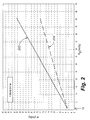
- load line 204 is derived by superimposing two surface plots, with their intersection being the load line for a given notch filter center frequency fn.
- One of the surface plots is a plot of the achievable resonant frequencies as a function of the width w of trace 106 and the depth h g of the reference return path. This surface plot is for a given fixed capacitance of 27 pF in this example.
- h l (30 + h g ) mils.
- a reference plane is superimposed onto the aforementioned first surface plot.
- This reference plane is the desired notch filter resonant frequency f n of 1 GHz in this example.
- the intersection of these two surfaces is line 204 that highlights the needed width of trace 106 as a function of the depth h g of ground plane 122 within printed circuit board 120.
- the 27 pF 0603-type capacitor is currently believed to be the only capacitor that will provide a 1 GHz notch filter for any depth of ground plane 122 within a conventional 62 mil thick printed circuit board 120 .
- the depth h g of ground plane 122 must be greater than some minimal depth, or will only work within some subset of the entire 62 mil PCB thickenss.
- a plurality of capacitors can be connected in parallel to form capacitor 102, and one or more of those capacitors can carry traces that together, in parallel, form trace 106. If capacitors of slightly-different values are used in parallel, the result is a plurality of slightly-different notch filters - or, equivalently, a notch filter having a wider notch - resuting in improved EMI attenuation.
- One of the advantages of a notch filter 100 constructed in the illustrative manner is that it occupies a very small amount of PCB real estate.
- the capacitors may be vertically stacked, illustratively as described in U.S. patent aplication serial no. 10/292,670, filed on November 12, 2002, and assigned to the same assignee as this application.
- a 23 pF 0603-type capacitor may be used in parallel with the 27 pF capacitor.
- the load line for the parallel combination of the 23 pF and 27 pF capacitors is shown as load line 202 in Fig. 2.
- Fig. 3 shows a load line 304 for a surface-mountable 0402-type capacitor (length of 40 mils, width and height of 20 mils) of 1.7 pF used to implement a 4.8 GHz notch filter.
- the 1.7 pF capacitor may advantageously be used in parallel with a 0402-type capacitor of 1.508 pF to implement the 4.8 GHz notch filter.
- the load line for the parallel combination of the two capacitors is shown as load line 302 in Fig. 3.
- Fig. 3 shows a load line 304 for a surface-mountable 0402-type capacitor (length of 40 mils, width and height of 20 mils) of 1.7 pF used to implement a 4.8 GHz notch filter.
- the 1.7 pF capacitor may advantageously be used in parallel with a 0402-type capacitor of 1.508 pF to implement the 4.8 GHz notch filter.
- the load line for the parallel combination of the two capacitors is shown as load line 302 in Fig. 3.
- the load line for the parallel combination of the two capacitors is shown as load line 402 in Fig. 4.
Landscapes
- Physics & Mathematics (AREA)
- Electromagnetism (AREA)
- Engineering & Computer Science (AREA)
- Microelectronics & Electronic Packaging (AREA)
- Filters And Equalizers (AREA)
- Control Of Motors That Do Not Use Commutators (AREA)
Applications Claiming Priority (2)
| Application Number | Priority Date | Filing Date | Title |
|---|---|---|---|
| US661137P | 2003-09-12 | ||
| US10/661,137 US7427904B2 (en) | 2003-09-12 | 2003-09-12 | Ultra-high-frequency notch filter having an inductance set by selecting a conductor width |
Publications (1)
| Publication Number | Publication Date |
|---|---|
| EP1517441A2 true EP1517441A2 (de) | 2005-03-23 |
Family
ID=34227068
Family Applications (1)
| Application Number | Title | Priority Date | Filing Date |
|---|---|---|---|
| EP04250563A Withdrawn EP1517441A2 (de) | 2003-09-12 | 2004-02-03 | Ultrahochfrequenz-Kerbfilter |
Country Status (7)
| Country | Link |
|---|---|
| US (1) | US7427904B2 (de) |
| EP (1) | EP1517441A2 (de) |
| JP (1) | JP2005094730A (de) |
| KR (1) | KR100702751B1 (de) |
| CN (1) | CN1595797A (de) |
| CA (1) | CA2457252A1 (de) |
| MX (1) | MXPA04008642A (de) |
Families Citing this family (19)
| Publication number | Priority date | Publication date | Assignee | Title |
|---|---|---|---|---|
| JP4850518B2 (ja) * | 2006-01-18 | 2012-01-11 | 株式会社日立製作所 | 電源回路及びそれを用いた映像表示装置 |
| EP2349453A4 (de) * | 2008-10-30 | 2015-07-01 | Greatbatch Ltd | Physikalisch seriell angeordnete kondensator- sowie induktorelemente mit parallel geschalteten konzentrierten parametern zur formung eines kerbfilters |
| US9699278B2 (en) | 2013-06-06 | 2017-07-04 | Zih Corp. | Modular location tag for a real time location system network |
| US11423464B2 (en) | 2013-06-06 | 2022-08-23 | Zebra Technologies Corporation | Method, apparatus, and computer program product for enhancement of fan experience based on location data |
| US10437658B2 (en) | 2013-06-06 | 2019-10-08 | Zebra Technologies Corporation | Method, apparatus, and computer program product for collecting and displaying sporting event data based on real time data for proximity and movement of objects |
| US9517417B2 (en) | 2013-06-06 | 2016-12-13 | Zih Corp. | Method, apparatus, and computer program product for performance analytics determining participant statistical data and game status data |
| US10609762B2 (en) | 2013-06-06 | 2020-03-31 | Zebra Technologies Corporation | Method, apparatus, and computer program product improving backhaul of sensor and other data to real time location system network |
| US9715005B2 (en) | 2013-06-06 | 2017-07-25 | Zih Corp. | Method, apparatus, and computer program product improving real time location systems with multiple location technologies |
| US20140365194A1 (en) | 2013-06-06 | 2014-12-11 | Zih Corp. | Method, apparatus, and computer program product for dynamics/kinetics model selection |
| WO2015094214A1 (en) * | 2013-12-18 | 2015-06-25 | Intel Corporation | Ground routing device and method |
| US9661455B2 (en) | 2014-06-05 | 2017-05-23 | Zih Corp. | Method, apparatus, and computer program product for real time location system referencing in physically and radio frequency challenged environments |
| US20150375083A1 (en) | 2014-06-05 | 2015-12-31 | Zih Corp. | Method, Apparatus, And Computer Program Product For Enhancement Of Event Visualizations Based On Location Data |
| DE112015002651B4 (de) | 2014-06-05 | 2023-02-16 | Zebra Technologies Corporation | Systeme, Vorrichtung und Verfahren zur Ratenvariablen Ultrabreitbandkommunikation |
| WO2015186044A1 (en) | 2014-06-05 | 2015-12-10 | Zih Corp. | Receiver processor for adaptive windowing and high-resolution toa determination in a multiple receiver target location system |
| US10261169B2 (en) | 2014-06-05 | 2019-04-16 | Zebra Technologies Corporation | Method for iterative target location in a multiple receiver target location system |
| US9626616B2 (en) | 2014-06-05 | 2017-04-18 | Zih Corp. | Low-profile real-time location system tag |
| US9668164B2 (en) | 2014-06-05 | 2017-05-30 | Zih Corp. | Receiver processor for bandwidth management of a multiple receiver real-time location system (RTLS) |
| WO2015186043A1 (en) | 2014-06-06 | 2015-12-10 | Zih Corp. | Method, apparatus, and computer program product improving real time location systems with multiple location technologies |
| US9759803B2 (en) | 2014-06-06 | 2017-09-12 | Zih Corp. | Method, apparatus, and computer program product for employing a spatial association model in a real time location system |
Family Cites Families (11)
| Publication number | Priority date | Publication date | Assignee | Title |
|---|---|---|---|---|
| US5186647A (en) * | 1992-02-24 | 1993-02-16 | At&T Bell Laboratories | High frequency electrical connector |
| JPH0673901U (ja) * | 1993-03-18 | 1994-10-18 | 株式会社村田製作所 | 誘電体フィルタ |
| JP3438859B2 (ja) * | 1996-11-21 | 2003-08-18 | ティーディーケイ株式会社 | 積層型電子部品とその製造方法 |
| US5952607A (en) * | 1997-01-31 | 1999-09-14 | Lucent Technologies Inc. | Local area network cabling arrangement |
| US6211754B1 (en) * | 1997-06-04 | 2001-04-03 | Sanyo Electric Co., Ltd, | Integrated resonance circuit consisting of a parallel connection of a microstrip line and a capacitor |
| US6094112A (en) | 1997-10-15 | 2000-07-25 | Avx Corporation | Surface mount filter device |
| KR19990049687A (ko) * | 1997-12-15 | 1999-07-05 | 이형도 | 듀플렉스 유전체 필터 |
| JP3548821B2 (ja) * | 1999-05-10 | 2004-07-28 | 株式会社村田製作所 | 積層コンデンサ、ならびにこれを用いた電子装置および高周波回路 |
| US6539253B2 (en) * | 2000-08-26 | 2003-03-25 | Medtronic, Inc. | Implantable medical device incorporating integrated circuit notch filters |
| KR20010000674A (ko) | 2000-10-12 | 2001-01-05 | 박병우 | 분포선로를 이용한 lc 공진 안테나 |
| KR100802570B1 (ko) * | 2002-02-07 | 2008-02-13 | 엘지이노텍 주식회사 | 멀티레이어 필터장치 |
-
2003
- 2003-09-12 US US10/661,137 patent/US7427904B2/en not_active Expired - Fee Related
-
2004
- 2004-02-03 EP EP04250563A patent/EP1517441A2/de not_active Withdrawn
- 2004-02-09 CA CA002457252A patent/CA2457252A1/en not_active Abandoned
- 2004-03-10 JP JP2004066514A patent/JP2005094730A/ja not_active Abandoned
- 2004-09-06 MX MXPA04008642A patent/MXPA04008642A/es active IP Right Grant
- 2004-09-07 CN CNA2004100768192A patent/CN1595797A/zh active Pending
- 2004-09-10 KR KR1020040072390A patent/KR100702751B1/ko not_active Expired - Fee Related
Also Published As
| Publication number | Publication date |
|---|---|
| KR20050027049A (ko) | 2005-03-17 |
| US7427904B2 (en) | 2008-09-23 |
| US20050059998A1 (en) | 2005-03-17 |
| CN1595797A (zh) | 2005-03-16 |
| MXPA04008642A (es) | 2004-12-09 |
| CA2457252A1 (en) | 2005-03-12 |
| JP2005094730A (ja) | 2005-04-07 |
| KR100702751B1 (ko) | 2007-04-03 |
Similar Documents
| Publication | Publication Date | Title |
|---|---|---|
| EP1517441A2 (de) | Ultrahochfrequenz-Kerbfilter | |
| EP1354502B1 (de) | Hochfrequenzleiterplattenkontaktlocher | |
| KR100638755B1 (ko) | 집적 회로 인터페이스용 필터 구조물 | |
| US5801602A (en) | Isolation and signal filter transformer | |
| CN101453828B (zh) | 电磁带隙结构与印刷电路板 | |
| US8314663B2 (en) | Directional coupler | |
| US9947979B2 (en) | High-frequency filter and electronic device | |
| US20090033439A1 (en) | Multilayer filter | |
| EP2466999A1 (de) | Leiterplatte | |
| US6297965B1 (en) | Wiring arrangement including capacitors for suppressing electromagnetic wave radiation from a printed circuit board | |
| US8283990B2 (en) | Signal transmission communication unit and coupler | |
| US5912597A (en) | Printed circuit board | |
| CN101610636A (zh) | 电磁带隙结构及印刷电路板 | |
| JP2007180073A (ja) | フィルタ素子 | |
| US5760662A (en) | Methods and apparatus for improving frequency response of integrated RC filters with additional ground pins | |
| CN113114382B (zh) | 电源滤波的装置 | |
| JPH1197962A (ja) | 高周波部品 | |
| US6879223B2 (en) | Distributed constant type filter | |
| US8508317B2 (en) | Broadband coupling filter | |
| Yoon et al. | NOrte et al. | |
| CN211352595U (zh) | 一种射频印刷电路板、射频装置及终端设备 | |
| JPH1022703A (ja) | 誘電体フィルタ | |
| US20060274478A1 (en) | Etched capacitor laminate for reducing electrical noise | |
| JP2006101149A (ja) | 積層型分波器 | |
| JP2005184244A (ja) | 結合装置及び高周波モジュール |
Legal Events
| Date | Code | Title | Description |
|---|---|---|---|
| PUAI | Public reference made under article 153(3) epc to a published international application that has entered the european phase |
Free format text: ORIGINAL CODE: 0009012 |
|
| AK | Designated contracting states |
Kind code of ref document: A2 Designated state(s): AT BE BG CH CY CZ DE DK EE ES FI FR GB GR HU IE IT LI LU MC NL PT RO SE SI SK TR |
|
| AX | Request for extension of the european patent |
Extension state: AL LT LV MK |
|
| STAA | Information on the status of an ep patent application or granted ep patent |
Free format text: STATUS: THE APPLICATION IS DEEMED TO BE WITHDRAWN |
|
| 18D | Application deemed to be withdrawn |
Effective date: 20090303 |