EP1517333A1 - Zustandskennzeichen (Flag) für einen bezüglich Löschen und Schreiben asymmetrischen Speicher - Google Patents
Zustandskennzeichen (Flag) für einen bezüglich Löschen und Schreiben asymmetrischen Speicher Download PDFInfo
- Publication number
- EP1517333A1 EP1517333A1 EP04018551A EP04018551A EP1517333A1 EP 1517333 A1 EP1517333 A1 EP 1517333A1 EP 04018551 A EP04018551 A EP 04018551A EP 04018551 A EP04018551 A EP 04018551A EP 1517333 A1 EP1517333 A1 EP 1517333A1
- Authority
- EP
- European Patent Office
- Prior art keywords
- state
- flag
- memory
- value
- switching
- Prior art date
- Legal status (The legal status is an assumption and is not a legal conclusion. Google has not performed a legal analysis and makes no representation as to the accuracy of the status listed.)
- Granted
Links
- 230000015654 memory Effects 0.000 title claims abstract description 146
- 238000000034 method Methods 0.000 claims abstract description 44
- 238000012217 deletion Methods 0.000 claims description 13
- 230000037430 deletion Effects 0.000 claims description 13
- 230000000694 effects Effects 0.000 claims description 2
- XUIMIQQOPSSXEZ-UHFFFAOYSA-N Silicon Chemical compound [Si] XUIMIQQOPSSXEZ-UHFFFAOYSA-N 0.000 description 1
- 101150074062 Tnfsf11 gene Proteins 0.000 description 1
- 230000003139 buffering effect Effects 0.000 description 1
- 238000010276 construction Methods 0.000 description 1
- 230000001419 dependent effect Effects 0.000 description 1
- 238000005516 engineering process Methods 0.000 description 1
- 229910052710 silicon Inorganic materials 0.000 description 1
- 239000010703 silicon Substances 0.000 description 1
- 230000002123 temporal effect Effects 0.000 description 1
Images
Classifications
-
- G—PHYSICS
- G11—INFORMATION STORAGE
- G11C—STATIC STORES
- G11C16/00—Erasable programmable read-only memories
- G11C16/02—Erasable programmable read-only memories electrically programmable
- G11C16/06—Auxiliary circuits, e.g. for writing into memory
- G11C16/10—Programming or data input circuits
- G11C16/14—Circuits for erasing electrically, e.g. erase voltage switching circuits
- G11C16/16—Circuits for erasing electrically, e.g. erase voltage switching circuits for erasing blocks, e.g. arrays, words, groups
-
- G—PHYSICS
- G11—INFORMATION STORAGE
- G11C—STATIC STORES
- G11C16/00—Erasable programmable read-only memories
- G11C16/02—Erasable programmable read-only memories electrically programmable
- G11C16/06—Auxiliary circuits, e.g. for writing into memory
- G11C16/10—Programming or data input circuits
Definitions
- the invention relates to a memory device having a plurality of Memory cells having, with respect to the writing and erasing asymmetric electronic memory with at least one in the memory Implemented state flag (Flag), which optionally has a first (set, valid) state value or a second (not set, invalid) state value, and that between the first and the second state value is switchable.
- Flag Implemented state flag
- An electronic memory is usually in a plurality of memory cells divided.
- the individual memory cells of one first memory state for example, a logic "1" in one second memory state, for example a logical "0", and vice versa, for which deletions and writes are performed.
- Which state of the deleted and the described memory state while a logical "1" and which is a logical "0" is usually freely selectable and is usually already by the manufacturer of the store established.
- a plurality of electronic memories are related to writing and erasing data asymmetric, for example, by the time taken to clear the Memory is required (erase time or erase duration), is different the amount of time required to write to the memory (Writing time or writing time).
- the power consumption be different from the power consumption when writing Clear.
- the programming voltage is which has to be created for programming, different, depending on whether the memory is written or deleted. Under the programming voltage is actually the memory cell to understand voltage applied from an external, from a voltage source generated voltage used to generate the programming voltage used can be different.
- a state flag or equivalent flag marked For different operations, such as programming operations, in a memory, it is necessary that the state of a predetermined Memory section is known, so that, for example, the condition as a condition can be used for subsequent operation steps.
- a state flag or equivalent flag marked On the state value (Flag value) may be, for example, writing (or reading) in the memory section either forbidden or allowed.
- Subject of the invention is a state flag or flag in this sense, ie a flag through which a state is indicated.
- atomic writes which are distinguished by being only either complete or not at all.
- An example of such atomic writing represents the writing of data into a smart card for example, to update a misoperation counter or to charge an electronic purse with a payment (Rankl, Effing, Handbuch der Chip Actually, 4th edition, Carl Hanser Verlag Kunststoff Vienna, 2002, chapter 5.10 "Atomic Processes", pp. 293-295). Should new data in a memory section of the smart card will be written first the original data before writing in the memory section stored in a non-volatile buffer memory of the smart card copied (e.g., into an EEPROM memory of the smart card).
- the state flag or flag has a valid one in this case State value.
- the new data e.g., new amount of money in the electronic purse, which is equal to the original one Amount of money reduced by the amount to be paid
- a conventional state flag consists of a single state flag Memory cell, e.g. a single bit set to zero "0" or one "1" is, depending on whether the state value of the state flag (flags) valid (Flag set) or invalid (flag not set).
- the object of the invention is a memory device of the aforementioned To create a way to more efficiently switch the state flag allows, and a corresponding identification method using to create a condition indicator.
- the memory device according to the invention according to the independent claim 1 has an electronic memory with a plurality of binary Memory cells.
- Each memory cell is through a programming process between a cleared and a described state switchable, wherein can be produced by a deletion of the deleted state and by a write operation of the described state can be produced.
- the memory is asymmetric with respect to writes and erasures, where this means in more detail that one or more Programming parameters have a different (different) value than during a deletion process.
- the programming parameters can include: the programming time, i. the amount of time it takes to get one complete programming process, in particular writing or Deletion process, perform; the programming voltage, i. the voltage, which are applied to the memory, in particular to each individual memory cell must be to perform a programming operation.
- the storage device has a switching device, with the value of the state flag between the first and the second state value is switchable, wherein for switching the state value at least one programming operation on at least one memory cell is carried out.
- the switching device, with the the value of the state flag is switched i. optionally set and delete, can be implemented such that the switching from the first to second state value and for switching from the second to the first state value the same kind of programming process, in particular Write or delete operation is performed.
- the switching device with the the value of the state flag is switched, i. optionally set and delete
- both for setting the flag and for deleting the flag a write operation is performed on a memory cell.
- both for setting the flag as well as for deleting the flag an erase operation performed on a memory cell.
- the memory device has the advantage that the state identifier (Flag) with respect to its placement and deletion symmetric is. That In particular, they have one or more programming parameters such as programming time and / or programming voltage at erase and when setting the same value. This requires no case distinction after that, whether the state flag (flag) is set or cleared, leaving a switching device with a simple Construction can be used. Switching the state flag This makes it more efficient than known storage devices.
- a memory device which is a enables more efficient switching of the state flag.
- the memory may for example be an (ordinary) EEPROM or a flash EEPROM (Flash ROM), which in the above sense asymmetric is.
- the components of the storage device according to the invention such as the state identifier and the switching device, in software form, in Hardware form or partly implemented in software form, partly in hardware form be.
- the state flag and the switching device and optionally implemented further components in software form.
- the asymmetry regarding writes and deletes includes according to an embodiment of the invention, that a write operation a has shorter programming time (shorter) than a deletion or vice versa.
- a write operation a has shorter programming time (shorter) than a deletion or vice versa.
- the switching device for switching between the first and second state values of the state flag (Flag) of that programming operation of the Write operation and the deletion process is used, which is a shorter Programming duration has.
- This preferred embodiment has the following Advantage, that the state flag for switching its state value only "fast" programming operations used. This is the result Condition indicator particularly time-saving and therefore efficient.
- the asymmetry comprises regarding writes and deletions that a Write another, different (higher or lower) program voltage needed as a deletion.
- the Switching the state flag of that programming process used which requires the lower programming voltage is particularly energy efficient when switching its state value.
- the memory device further has a reset device, with which an initial state of the state flag is adjustable.
- Starting from the initial state is at least one switching operation to Switching, in particular setting or deleting, the state identifier (Flag) possible.
- the state identifier Flag
- the state flag is one from the initial state Plural of successive switching operations possible in which the state value of the state flag alternately between valid and is invalidated, i. alternately always from invalid becomes valid and is switched from valid to invalid once. In doing so, according to the invention, for switching in each case the same type of programming operation used, regardless of whether the state flag is switched to valid or invalid.
- the reset device is further preferably implemented such that to set the initial state, the other programming operation used by the write and delete operations when he was to Switching between the first and second state values of the state flag (Flag) is used.
- for switching the state flag (Flag) uses the faster programming process, in which the programming time is lower, whereas to set the Initial state by means of the reset means the slower programming operation is used, where the programming time is higher is.
- This embodiment has the further advantage that the slow Programming procedure is used exclusively on reset, the is usually performed less frequently than switching the state flag (Flag). When usually more frequently performed switching the state flag (Flag), i. when setting and clearing, the fast Programming process used.
- for switching the state flag (Flag) uses the more power-saving programming process in which a lower programming voltage can be applied to the memory cell (s) whereas, to set the initial state by means of the reset means the more power-intensive programming process is used, where a higher programming voltage is applied to the memory cell (s) must become. This is the power-intensive programming process only in the less frequent reset of the flag (Flag) in use, when switching (setting, clearing) the state flag (flag) is against the power-saving programming process used.
- a preferred use of the memory device according to the invention is in a disk like a smart card or token, with a electronic circuit in which the memory device is implemented.
- the smart card may be a contactless or contact-based or both contactless as well as contact-based smart card with any Format, e.g. according to ISO 7810, e.g. ID-1 (check card format) or ID-000 (SIM card or mini card format) or ID-00 or to GSM 11.1 or TS 102.221 or another standard, or no standard.
- the token can be any housing and any interface (contactless, contact-based, serial, USB, etc.).
- the state flag at least one pair of two sub-flags, each sub-code of the pair has at least one memory cell.
- the state indicator from Fig. 1 which is described in more detail below, forms a special form of such a state identifier, in which in particular each sub-label of the pair has the same number of memory cells, in particular eight.
- the partial identifiers of FIG. 1 are of individual memory cells each memory cell is one bit in size, so that each sub-tag is formed as a bit field B1 or B2.
- the individual memory cells have a size other than bits, for example
- each memory cell can be two bits or one byte in size.
- the number of Memory cells per sub-tag or bit field can also be higher or higher lower than eight.
- the number of memory cells per sub-label / Bit field unlike shown in Fig. 1, be different.
- the number of memory cells in both sub-flags the same, since in this case an alternating switching of the state flag (Flag) in the two partial identifiers / bit fields up to the last memory cell is possible.
- An inventive flash memory with the state identifier with the two sub-codes is preferably divided into pages, wherein the Deleting the memory one page at a time is deleted.
- Each of the both sub-flags preferably have a number in the flash memory of memory cells equal to an integer divider of page size (Number of memory cells per page), so that is a single page through an integer number of sub-flags can be completely filled.
- the size of the part identifier (number of memory cells in the part indicator) equal to an integer divisor of the half page size is, so that is a single page through an integer number of state flags can be completely filled with two partial identifiers.
- a state flag with a pair of (two) sub-flags is the first state value thereby excellent, that in each part mark of the pair the same number of memory cells the erased and / or the described state wherein the second state value in this embodiment is thereby it is excellent that in each sub-label of the pair a different Number of memory cells the deleted and / or described State has.
- the individual memory cells form the first part identifier with the individual memory cells of the second Part identifier pairs of corresponding memory cells, i. the first (second, third, fourth, ...) memory cell of the first sub-label corresponds with the first (second, third, fourth, ...) memory cell of the second Part mark.
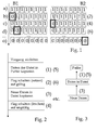
- Fig. 1 shows a state flag according to a preferred embodiment the invention.
- the status indicator (flag) consists of two bit fields B1, B2 each with eight bits.
- the first line a) of Fig. 1 shows the state flag in its Initial state in which it is after a reset by means of the reset device is not switched on again after resetting has been. All bits have the logical value "1", so both Bit fields B1, B2 have the same number of eight “ones” and zero "zeroes”. At the same time, each pair of corresponding bits (memory cells) of the two bit fields B1, B2 the same state, i.
- the first bit (from left) of the first bit field B1 has the same state as the first bit (from left) of the second bit field B2
- the second bit (from the left) of the first bit field B1 has the same state as the second bit (from the left) of the second bit field B2
- the third bit (from the left) of the first bit field B1 has the same State as the third bit (from left) of the second bit field B2 etc.
- the state value the state flag is not valid, i. the flag is deleted, i. not set.
- the second line b) of Fig. 1 shows the state flag after it has been set, i. after its state value is set to "set" has been.
- the first bit of the first bit field B1 (framed) switched from “1" to "0".
- the bit field B1 now has seven ones and a zero.
- the state value of the state flag is consequently valid or set.
- the first bit of the first bit field B1 (State value "0") has a different state than the first bit of the second bit field B2 (state value "1").
- the state flag (Flag) also according to set this criterion (valid).
- the third line c) of Fig. 1 shows the state flag after it, after being set from line b), has been deleted again, i. after its state value has been switched to not set (deleted) is.
- the first bit of the second bit field B2 (framed) is from "1" "0" has been switched.
- the first bit field B1 still has seven ones and a zero.
- the second bit field B2 now also has seven ones and a zero. Therefore, the two bit fields B1, B2 have the same number of Ones or zeros.
- the state value of the state flag is consequently invalid or not set.
- the first Bit of the first bit field B1 and the first bit of the second bit field B2 (again) the same condition.
- the first pair of corresponding bits thus has (again) the same state, so that all corresponding ones Bits (memory cells) have the same state.
- the fourth line d) of Fig. 1 shows the state flag after it, after deleting from line c), has been set again.
- the second bit of the first bit field B1 (framed) is switched from "1" to "0" Service. Therefore, the two bit fields B1, B2 have a different one Number of ones or zeros. The state value of the state flag is therefore invalid or not set.
- the second bit of the first bit field B1 (framed, state value "0") and the second bit of the second bit field B2 (state value "1") has a different one Status.
- the corresponding second bits of the two bit fields B1, B2 thus have a different state. All other corresponding pairs (first, third, fourth, ... eighth corresponding Pair) of bits each have the same state, namely left of current (here second) bit with state value "1", right of it with state value "0".
- the status code can be set six more times and be deleted seven times, a total of eight times, i. as often as each Bitfield Bits has to be set and cleared. It is alternately one bit in the first bit field B1 and one bit in the second bit field B2 switched. Within each individual bit field B1 or B2, the adjacent bits become switched in series, i. first the first bit, then the second bit, then the third bit, then the fourth bit etc. As the last bit becomes, as in the last one Line o) of Fig. 1, the last bit (framed) of the second bit field B2 switched. Only then are all bits set to "zero", and the state flag must be reset again (Reset) to the in Restore line a) of Fig. 1 state shown.
- a state identifier with two part identifier ie in particular for a state tag with two bit fields like the one shown in FIG. 1
- a state value of the state flag (Flag) has the memory device according to one embodiment of the invention, a logic unit, in particular an XOR logic unit.
- the logic unit is set up to corresponding memory cells of the first and second Part indicator and link the result of the link as state value of the state flag.
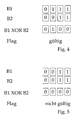
- FIGS. 4 and 5 illustrate the operation of a device according to the invention Logic unit in the form of an XOR logic unit.
- Fig. 4 shows the How an XOR logic unit works using the example of a valid (set) Flag.
- Fig. 5 shows the operation of the XOR logic unit by way of example an invalid (not set, deleted) flag.
- the first two lines FIGS. 4 and 5 each show a state flag with two Bit fields B1 and B2 according to a similar embodiment of the state flag like that shown in Figure 1, but with only four bits per bit field B1, B2.
- the flag of Fig. 4 is set (valid) because the second bit of the first memory field B1 has the state value "1" and the second bit of the second memory field B2 has the state value "0", so that is the two corresponding second bits have different state values.
- the bitwise XOR operation the two bit fields results in the one shown in the third line Bit sequence. Because one of the four bits, here the second bit, is different from zero is, the flag is considered set (valid), as shown in the fourth line. The flag would be considered set even if the third line contains another of the four bits, so the first, third or fourth bit, different from zero would be (not shown in Fig. 4).
- the flag of Fig. 5 is not set (invalid) because all four pairs of corresponding ones Bits have the same state value, namely "zero" for the both corresponding first bits and the two corresponding ones second bits, as well as "one" for the two corresponding third bits and the two corresponding fourth bits.
- the bitwise XOR operation the two bit fields results in the bit sequence shown in the third line. Since all bits are zero, the flag is considered not set (invalid) as in the fourth line is shown.
- Fig. 2 shows, according to an embodiment of the invention, the process flow when writing (copying) new data to a file, with previous Buffer the original data that was originally present in the file were.
- Fig. 3 shows schematically the temporal and spatial sequence the copying operations in the method of Fig. 2.
- a file contains original data. Well, you should into the file new data are copied and stored there, whereby the original data will be overwritten.
- To buffer the original one Data is a buffer available, which has a flag, with which the data in the buffer memory is marked as valid or invalid can.
- the process has been initiated, be in one first step (1) the original data of the file in the buffer memory copied (Fig. 2, Fig. 3).
- the Flag of the buffer set to valid (Fig. 2). This can be, for example by a switching operation (2) as shown in line b) of FIG in which the first bit of the first bit field B1 is switched becomes.
- the new data is copied to the file and stored there (Fig.
- a fourth step (4) the flag of the buffer memory set to invalid ( Figure 2).
- This can be done for example by a Switching operation (4) as shown in line c) of Fig. 1 are performed, in which the first bit of the second bit field B2 is switched.
- Occurs Process abort on while the flag is set will be on again Recording the process the data from the buffer into the file written. If, on the other hand, the occurrence of the abort is the flag deleted, when the procedure is re-recorded in the file Preserve existing data.
- a first step (5) the original data the file is copied to the buffer memory (Fig. 2, Fig. 3).
- the flag of the buffer is set to valid ( Figure 2). This can be done, for example, by a switching process (6) like that in Line d) of Fig. 1, in which the second bit of the first bit field B1 is switched.
- the memory means in addition, a reset security unit, which is set up is, the state flag for consistency according to a predetermined Structure that has the state flag to check.
- the reset protection unit can prevent the flag from being indefinite State obtained when during operation, e.g. during the Setting or resetting, an interruption occurs, in particular one Interruption of the supply voltage. Which state of the state flag is consistent and which is not, is due to the structure of the state flag predetermined.
- each with several logic linear e.g., as shown in Fig. 1, Fig. 4, 5
- the consistency preferably that within each sub-label at most a single pair of adjacent memory cells exists, the have different state values. In this way it is ensured that the memory cells have such values as they can by a proper bitwise, sequential write are generated in the adjacent Memory cells within a sub-tag in turn sequentially (i.e., in an order of first, second, third, etc. memory cell) be switched.
- the reset security unit is preferably further configured to to cause a reset of the state flag to the output value or to cause if the check results in a lack of consistency. If the reset is effected, preferably all are required Devices in the memory device available, and continue preferably in a data carrier such as a chip card or a token integrated. If the reset is merely caused, is optionally at least part of the facilities required to effect the reset provided separately from the memory device and, if the Storage device in a data carrier such as a chip card or a token is integrated, provided outside the data carrier.
- the status indicator becomes inconsistent recognized.
- the state flag becomes the initial value (e.g., "11111111").
- the memory cells are logical Seen next to each other, so they have a linear sequence of memory cells form, for example, a memory word or a plurality of memory words or the like, the memory cells being physically do not necessarily have to be next to each other.
- a write operation preferably has a write duration of the range from about 1 to about 20 ⁇ s, more preferably about typically 7 ⁇ s and a maximum of 10 ⁇ s, and an erase operation an erase duration the range of about 1 ms to about 50 ms, more preferably typically about 18 ms and a maximum of 25 ms, or vice versa.
- the Programming voltage is preferably for writing in the voltage range from 1V to 4V, preferably at about 3.0V to 3.6V and to extinguish in Voltage range of 5V to 16V, preferably about 10V, or vice versa.
- the programming voltage is preferably equal to that of the single memory cell applied voltage from that applied from the outside Voltage may be different, with the applied to the memory cell Voltage preferably in a conventional manner from the outside applied voltage is generated.
- the externally applied voltage is for example the output voltage of a voltage source.
- the mentioned Parameter values are example values. Depending on the used Memory, the parameter values can also be in other areas.
Landscapes
- Read Only Memory (AREA)
- Control Of Indicators Other Than Cathode Ray Tubes (AREA)
- Memory System Of A Hierarchy Structure (AREA)
- Dram (AREA)
- Memory System (AREA)
Abstract
Description
- Fig. 1
- ein Zustandskennzeichen (Flag) gemäß einer Ausführungsform der Erfindung, mit zwei Bitfeldern B1, B2;
- Fig. 2
- den Verfahrensablauf beim Schreiben (Kopieren) von neuen Daten in eine Datei, mit vorherigem Puffern der ursprünglichen Daten in der Datei, gemäß einer Verwendung der Erfindung;
- Fig. 3
- eine schematische Darstellung der Kopiervorgänge der ursprünglichen Daten von der Datei in den Pufferspeicher und der neuen Daten in die Datei, bei dem Verfahren aus Fig. 2;
- Fig. 4
- die Funktionsweise einer XOR-Logikeinheit zur Ermittlung des Zustandswerts eines Flag am Beispiel eines gültigen (gesetzten) Flag;
- Fig. 5
- die Funktionsweise der XOR-Logikeinheit aus Fig. 4 am Beispiel eines ungültigen (nicht gesetzten, gelöschten) Flag.
Claims (19)
- Speichereinrichtung mitwobei weiter die Schalteinrichtung derart implementiert ist, dass zum Schalten vom ersten zum zweiten Zustandswert und zum Schalten vom zweiten zum ersten Zustandswert die gleiche Art von Programmiervorgang, insbesondere Schreibvorgang oder Löschvorgang, durchgeführt wird.einem elektronischen Speicher mit einer Mehrzahl von binären Speicherzellen, wobei jede Speicherzelle durch einen Programmiervorgang zwischen einem gelöschten und einem beschriebenen Zustand schaltbar ist, wobei durch einen Löschvorgang der gelöschte Zustand herstellbar ist und durch einen Schreibvorgang der beschriebene Zustand herstellbar ist, wobei der Speicher bezüglich Schreibvorgängen und Löschvorgängen asymmetrisch ist,mindestens einem in dem Speicher implementierten Zustandskennzeichen (Flag), das wahlweise einen ersten, gesetzten (gültigen), Zustandswert oder einen zweiten, nicht gesetzten (ungültigen), Zustandswert haben kann, undeiner Schalteinrichtung, mit der der Wert des Zustandskennzeichens zwischen dem ersten und dem zweiten Zustandswert schaltbar ist, wobei zum Schalten des Zustandswerts mindestens ein Programmiervorgang an mindestens einer Speicherzelle durchgeführt wird,
- Speichereinrichtung nach Anspruch 1, wobei die Asymmetrie bezüglich Schreibvorgängen und Löschvorgängen umfasst, dass ein Schreibvorgang eine kürzere Programmierdauer hat (kürzer dauert) als ein Löschvorgang oder umgekehrt.
- Speichereinrichtung nach Anspruch 1 oder 2, wobei von der Schalteinrichtung zum Schalten zwischen dem ersten und zweiten Zustandswert des Zustandskennzeichens (Flag) derjenige Programmiervorgang von dem Schreibvorgang und dem Löschvorgang verwendet wird, der eine kürzere Programmierdauer hat.
- Speichereinrichtung nach einem der Ansprüche 1 bis 3, wobei die Asymmetrie bezüglich Schreibvorgängen und Löschvorgängen umfasst, dass ein Schreibvorgang eine andere, insbesondere höhere oder niedrigere, Programmierspannung, insbesondere für den Programmiervorgang an der Speicherzelle, benötigt als ein Löschvorgang.
- Speichereinrichtung nach einem der Ansprüche 1 bis 4, wobei das Zustandskennzeichen mindestens ein Paar von zwei Teilkennzeichen hat, wobei jedes Teilkennzeichen des Paars mindestens eine Speicherzelle aufweist.
- Speichereinrichtung nach Anspruch 5, wobei jedes Teilkennzeichen des Paars die gleiche Anzahl von Speicherzellen aufweist.
- Speichereinrichtung nach Anspruch 5 oder 6, wobei der erste Zustandswert des Zustandskennzeichens (Flag) dadurch ausgezeichnet ist, dass in jedem Teilkennzeichen des Paars von Teilkennzeichen die gleiche Anzahl von Speicherzellen den gelöschten und/ oder den beschriebenen Zustand hat, und wobei der zweite Zustandswert des Zustandskennzeichens (Flag) dadurch ausgezeichnet ist, dass in jedem Teilkennzeichen des Paars von Teilkennzeichen eine unterschiedliche Anzahl von Speicherzellen den gelöschten und/ oder den beschriebenen Zustand hat.
- Speichereinrichtung nach einem der Ansprüche 5 bis 7, wobei der erste Zustandswert des Zustandskennzeichens (Flag) dadurch ausgezeichnet ist, dass in den beiden Teilkennzeichen des Paars von Teilkennzeichen korrespondierende Speicherzellen den gleichen Zustand haben, und der zweite Zustandswert des Zustandskennzeichens (Flag) dadurch ausgezeichnet ist, dass für ein Paar von korrespondierenden Speicherzellen in den beiden Teilkennzeichen die beiden korrespondierenden Speicherzellen voneinander unterschiedliche Zustände haben.
- Speichereinrichtung nach einem der Ansprüche 5 bis 8, die eine, insbesondere in Softwareform und/oder in Hardwareform implementierte, Logikeinheit, insbesondere XOR-Logikeinheit, aufweist, die dazu eingerichtet ist, korrespondierende Speicherzellen des ersten und des zweiten Teilkennzeichens zu verknüpfen und das Ergebnis der Verknüpfung als Zustandswert des Zustandskennzeichens auszugeben oder für die weitere Berechnung des Zustandswerts bereitzustellen.
- Speichereinrichtung nach einem der Ansprüche 1 bis 9, die weiter eine Rücksetzeinrichtung aufweist, mit der ein Ausgangszustand des Zustandskennzeichens einstellbar ist.
- Speichereinrichtung nach Anspruch 10, wobei die Rücksetzeinrichtung derart implementiert ist, dass sie zum Einstellen des Ausgangszustands den anderen Programmiervorgang von dem Schreibvorgang und dem Löschvorgang verwendet, als er zum Schalten zwischen dem ersten und dem zweiten Zustandswert des Zustandskennzeichens (Flag) verwendet wird.
- Speichereinrichtung nach Anspruch 10 oder 11, die weiter eine Rücksetz-Absicherungseinheit aufweist, die dazu eingerichtet ist, das Zustandskennzeichen auf Konsistenz gemäß einer vorbestimmten Struktur, die das Zustandskennzeichen hat, zu überprüfen.
- Speichereinrichtung nach Anspruch 12, wobei die Rücksetz-Absicherungseinheit dazu eingerichtet ist, ein Rücksetzen des Zustandskennzeichens auf den Ausgangswert zu veranlassen oder zu bewirken, wenn die Überprüfung fehlende Konsistenz ergibt.
- Speichereinrichtung nach Anspruch 12 oder 13, wobei bei einem Zustandskennzeichen mit zwei Teilkennzeichen mit je mehreren logisch linear angeordneten Speicherzellen die Konsistenz umfasst, dass innerhalb jedes Teilkennzeichens höchstens ein einziges Paar von benachbarten Speicherzellen existiert, die unterschiedliche Zustandswerte haben.
- Datenträger, insbesondere Chipkarte oder Token, mit einem elektronischen Schaltkreis mit einer darin implementierten Speichereinrichtung nach einem der Ansprüche 1 bis 14.
- Verfahren zum Kennzeichnen des Zustands eines Speicherabschnitts, der insbesondere eine Datei oder ein Datenfeld oder vergleichbaren Speicherinhalt enthält, mittels eines Zustandskennzeichens, bei welchem Verfahrenwobei zum Schalten vom ersten zum zweiten Zustandswert und zum Schalten vom zweiten zum ersten Zustandswert die gleiche Art von Programmiervorgang, insbesondere Schreibvorgang oder Löschvorgang, durchgeführt wird.dem Speicherabschnitt eine nach einem der Ansprüche 1 bis 14 gestaltete Speichereinrichtung mit einem darin implementierten Zustandskennzeichen (Flag) bereitgestellt wird undin Abhängigkeit vom Zustand des Speicherabschnitts das Zustandskennzeichen auf einen ersten (gesetzten, gültigen) Zustandswert oder einen zweiten (nicht gesetzten, ungültigen) Zustandswert geschaltet wird,
- Verfahren nach Anspruch 16, wobei nach einmaligem oder mehrmaligem Schalten das Zustandskennzeichen auf einen Ausgangswert zurückgesetzt wird, wobei vorzugsweise das Rücksetzen mittels der anderen Art von Programmiervorgang von dem Schreibvorgang und dem Löschvorgang durchgeführt wird, als er zum Schalten verwendet wird.
- Verfahren nach Anspruch 17, wobei weiter eine Konsistenzprüfung durchgeführt wird, bei der das Zustandskennzeichen auf Konsistenz gemäß einer vorbestimmten Struktur, die das Zustandskennzeichen hat, überprüft wird.
- Verfahren nach Anspruch 18, wobei, wenn die Konsistenzprüfung fehlende Konsistenz ergibt, ein Rücksetzen des Zustandskennzeichens auf den Ausgangswert veranlasst oder bewirkt wird.
Applications Claiming Priority (2)
| Application Number | Priority Date | Filing Date | Title |
|---|---|---|---|
| DE10336225A DE10336225B3 (de) | 2003-08-07 | 2003-08-07 | Zustandskennzeichen (Flag) für einen bezüglich Löschen und Schreiben asymmetrischen Speicher |
| DE10336225 | 2003-08-07 |
Publications (2)
| Publication Number | Publication Date |
|---|---|
| EP1517333A1 true EP1517333A1 (de) | 2005-03-23 |
| EP1517333B1 EP1517333B1 (de) | 2009-12-30 |
Family
ID=33521553
Family Applications (1)
| Application Number | Title | Priority Date | Filing Date |
|---|---|---|---|
| EP04018551A Expired - Lifetime EP1517333B1 (de) | 2003-08-07 | 2004-08-05 | Zustandskennzeichen (Flag) für einen bezüglich Löschen und Schreiben asymmetrischen Speicher |
Country Status (3)
| Country | Link |
|---|---|
| EP (1) | EP1517333B1 (de) |
| AT (1) | ATE453913T1 (de) |
| DE (2) | DE10336225B3 (de) |
Cited By (1)
| Publication number | Priority date | Publication date | Assignee | Title |
|---|---|---|---|---|
| DE102007059142B3 (de) * | 2007-12-07 | 2008-10-30 | Giesecke & Devrient Gmbh | Verfahren zum Speichern eines Datums in einer Speichereinrichtung und Speichereinrichtung |
Families Citing this family (1)
| Publication number | Priority date | Publication date | Assignee | Title |
|---|---|---|---|---|
| CN115620789A (zh) * | 2022-09-29 | 2023-01-17 | 武汉新芯集成电路制造有限公司 | 存储芯片 |
Citations (3)
| Publication number | Priority date | Publication date | Assignee | Title |
|---|---|---|---|---|
| FR2725055A1 (fr) * | 1994-09-28 | 1996-03-29 | Trt Telecom Radio Electr | Dispositif de calculs d'operations modulaires et carte a puce comportant un tel dispositif |
| US5996041A (en) * | 1995-11-10 | 1999-11-30 | Samsung Electronics Co., Ltd. | Integrated circuit memory devices having page flag cells which indicate the true or non-true state of page data therein and methods of operating the same |
| US20030128646A1 (en) * | 2002-01-09 | 2003-07-10 | Peter Nangle | Asymmetrical programming mechanism for non-volatile memory |
Family Cites Families (1)
| Publication number | Priority date | Publication date | Assignee | Title |
|---|---|---|---|---|
| SE320230B (de) * | 1968-03-11 | 1970-02-02 | Saab Scania Ab |
-
2003
- 2003-08-07 DE DE10336225A patent/DE10336225B3/de not_active Expired - Fee Related
-
2004
- 2004-08-05 DE DE502004010577T patent/DE502004010577D1/de not_active Expired - Lifetime
- 2004-08-05 AT AT04018551T patent/ATE453913T1/de not_active IP Right Cessation
- 2004-08-05 EP EP04018551A patent/EP1517333B1/de not_active Expired - Lifetime
Patent Citations (3)
| Publication number | Priority date | Publication date | Assignee | Title |
|---|---|---|---|---|
| FR2725055A1 (fr) * | 1994-09-28 | 1996-03-29 | Trt Telecom Radio Electr | Dispositif de calculs d'operations modulaires et carte a puce comportant un tel dispositif |
| US5996041A (en) * | 1995-11-10 | 1999-11-30 | Samsung Electronics Co., Ltd. | Integrated circuit memory devices having page flag cells which indicate the true or non-true state of page data therein and methods of operating the same |
| US20030128646A1 (en) * | 2002-01-09 | 2003-07-10 | Peter Nangle | Asymmetrical programming mechanism for non-volatile memory |
Cited By (1)
| Publication number | Priority date | Publication date | Assignee | Title |
|---|---|---|---|---|
| DE102007059142B3 (de) * | 2007-12-07 | 2008-10-30 | Giesecke & Devrient Gmbh | Verfahren zum Speichern eines Datums in einer Speichereinrichtung und Speichereinrichtung |
Also Published As
| Publication number | Publication date |
|---|---|
| EP1517333B1 (de) | 2009-12-30 |
| ATE453913T1 (de) | 2010-01-15 |
| DE10336225B3 (de) | 2005-01-13 |
| DE502004010577D1 (de) | 2010-02-11 |
Similar Documents
| Publication | Publication Date | Title |
|---|---|---|
| DE69811254T2 (de) | Sicherer speicher mit multiplen sicherheitsebenen | |
| DE69809527T2 (de) | Externe Speichervorrichtung und Datenverarbeitungsverfahren | |
| DE69430668T2 (de) | Flash-speicher mit verringerter löschung und überschreibung | |
| DE4309814C2 (de) | Nichtflüchtige Halbleiterspeichervorrichtung | |
| EP1089219B1 (de) | Verfahren zur Sicherung eines Datenspeichers | |
| DE10159901B4 (de) | Mikrocomputer mit eingebautem programmierbarem, nichtflüchtigem Speicher | |
| DE69609256T2 (de) | Sicheres aktualisierungsverfahren für eeprom | |
| DE69317937T2 (de) | Nichtflüchtige Halbleiterspeicheranordnung | |
| EP0067364B1 (de) | Verfahren und Anordnung zum nichtflüchtigen Speichern des Zählerstandes einer elektronischen Zählschaltung | |
| DE102009033961A1 (de) | Emulation eines einmal programmierbaren Speichers | |
| DE69620334T2 (de) | Elektronisches Bauelement mit einem elektrisch löschbaren und nichtflüchtigen Speicher | |
| EP0123177B1 (de) | Verfahren zum Betreiben eines als nichtflüchtigen Schreib-Lese-Speichers ausgebildeten Anwendungsspeichers und Anordnung zur Durchführung des Verfahrens | |
| DE3025044C2 (de) | ||
| DE4302553A1 (en) | High security binary counting method for chip card - offsetting final state of binary number w.r.t. sequence such that contents of counter never represents number smaller than previous value | |
| EP1517333B1 (de) | Zustandskennzeichen (Flag) für einen bezüglich Löschen und Schreiben asymmetrischen Speicher | |
| DE602004008170T2 (de) | Speicherschaltung mit nichtflüchtigem Identifikationsspeicher und zugehöriges Verfahren | |
| EP1308842B1 (de) | Verfahren und Vorrichtung zur Verwaltung eines Datenspeichers | |
| EP1564754B1 (de) | Verfahren und Vorrichtung zur Verwaltung von Daten in einem nichtflüchtigen Datenspeicher | |
| DE69820080T2 (de) | Verfahren zum schreiben von binären datenwörtern mittels elektrisch-programmierbarer und löschbarer speicherzellen | |
| EP0214390A1 (de) | Freigabeverfahren für einen zugriffskontrollierten Anwenderspeicher und Anordnung zur Durchführung des Verfahrens | |
| EP2312444B1 (de) | Verfahren zum Schreiben von Datensätzen in einen nicht-flüchtigen Datenspeicher | |
| DE69936574T2 (de) | Verfahren für ein sicheres einheitszahlungsmanagement und zugehörige sicherheitsvorrichtung | |
| DE4220877A1 (de) | Verfahren für nichtflüchtige, lösch- und programmierbare Speichereinrichtungen | |
| DE19738712C2 (de) | Nichtflüchtiger Speicher mit zu Subblöcken zusammengefaßten Speicherzellen | |
| DE10317147A1 (de) | Sicheres Speichersystem mit Flash-Speichern und Cache-Speicher |
Legal Events
| Date | Code | Title | Description |
|---|---|---|---|
| PUAI | Public reference made under article 153(3) epc to a published international application that has entered the european phase |
Free format text: ORIGINAL CODE: 0009012 |
|
| AK | Designated contracting states |
Kind code of ref document: A1 Designated state(s): AT BE BG CH CY CZ DE DK EE ES FI FR GB GR HU IE IT LI LU MC NL PL PT RO SE SI SK TR |
|
| AX | Request for extension of the european patent |
Extension state: AL HR LT LV MK |
|
| 17P | Request for examination filed |
Effective date: 20050923 |
|
| AKX | Designation fees paid |
Designated state(s): AT BE BG CH CY CZ DE DK EE ES FI FR GB GR HU IE IT LI LU MC NL PL PT RO SE SI SK TR |
|
| 17Q | First examination report despatched |
Effective date: 20051121 |
|
| GRAP | Despatch of communication of intention to grant a patent |
Free format text: ORIGINAL CODE: EPIDOSNIGR1 |
|
| GRAJ | Information related to disapproval of communication of intention to grant by the applicant or resumption of examination proceedings by the epo deleted |
Free format text: ORIGINAL CODE: EPIDOSDIGR1 |
|
| GRAP | Despatch of communication of intention to grant a patent |
Free format text: ORIGINAL CODE: EPIDOSNIGR1 |
|
| GRAS | Grant fee paid |
Free format text: ORIGINAL CODE: EPIDOSNIGR3 |
|
| GRAA | (expected) grant |
Free format text: ORIGINAL CODE: 0009210 |
|
| AK | Designated contracting states |
Kind code of ref document: B1 Designated state(s): AT BE BG CH CY CZ DE DK EE ES FI FR GB GR HU IE IT LI LU MC NL PL PT RO SE SI SK TR |
|
| REG | Reference to a national code |
Ref country code: GB Ref legal event code: FG4D Free format text: NOT ENGLISH |
|
| REG | Reference to a national code |
Ref country code: CH Ref legal event code: EP |
|
| REG | Reference to a national code |
Ref country code: IE Ref legal event code: FG4D |
|
| REF | Corresponds to: |
Ref document number: 502004010577 Country of ref document: DE Date of ref document: 20100211 Kind code of ref document: P |
|
| PG25 | Lapsed in a contracting state [announced via postgrant information from national office to epo] |
Ref country code: SE Free format text: LAPSE BECAUSE OF FAILURE TO SUBMIT A TRANSLATION OF THE DESCRIPTION OR TO PAY THE FEE WITHIN THE PRESCRIBED TIME-LIMIT Effective date: 20091230 Ref country code: FI Free format text: LAPSE BECAUSE OF FAILURE TO SUBMIT A TRANSLATION OF THE DESCRIPTION OR TO PAY THE FEE WITHIN THE PRESCRIBED TIME-LIMIT Effective date: 20091230 |
|
| REG | Reference to a national code |
Ref country code: NL Ref legal event code: VDEP Effective date: 20091230 |
|
| PG25 | Lapsed in a contracting state [announced via postgrant information from national office to epo] |
Ref country code: PL Free format text: LAPSE BECAUSE OF FAILURE TO SUBMIT A TRANSLATION OF THE DESCRIPTION OR TO PAY THE FEE WITHIN THE PRESCRIBED TIME-LIMIT Effective date: 20091230 Ref country code: SI Free format text: LAPSE BECAUSE OF FAILURE TO SUBMIT A TRANSLATION OF THE DESCRIPTION OR TO PAY THE FEE WITHIN THE PRESCRIBED TIME-LIMIT Effective date: 20091230 |
|
| REG | Reference to a national code |
Ref country code: IE Ref legal event code: FD4D |
|
| PG25 | Lapsed in a contracting state [announced via postgrant information from national office to epo] |
Ref country code: RO Free format text: LAPSE BECAUSE OF FAILURE TO SUBMIT A TRANSLATION OF THE DESCRIPTION OR TO PAY THE FEE WITHIN THE PRESCRIBED TIME-LIMIT Effective date: 20091230 Ref country code: BG Free format text: LAPSE BECAUSE OF FAILURE TO SUBMIT A TRANSLATION OF THE DESCRIPTION OR TO PAY THE FEE WITHIN THE PRESCRIBED TIME-LIMIT Effective date: 20100330 Ref country code: ES Free format text: LAPSE BECAUSE OF FAILURE TO SUBMIT A TRANSLATION OF THE DESCRIPTION OR TO PAY THE FEE WITHIN THE PRESCRIBED TIME-LIMIT Effective date: 20100410 Ref country code: EE Free format text: LAPSE BECAUSE OF FAILURE TO SUBMIT A TRANSLATION OF THE DESCRIPTION OR TO PAY THE FEE WITHIN THE PRESCRIBED TIME-LIMIT Effective date: 20091230 Ref country code: NL Free format text: LAPSE BECAUSE OF FAILURE TO SUBMIT A TRANSLATION OF THE DESCRIPTION OR TO PAY THE FEE WITHIN THE PRESCRIBED TIME-LIMIT Effective date: 20091230 Ref country code: PT Free format text: LAPSE BECAUSE OF FAILURE TO SUBMIT A TRANSLATION OF THE DESCRIPTION OR TO PAY THE FEE WITHIN THE PRESCRIBED TIME-LIMIT Effective date: 20100430 |
|
| PG25 | Lapsed in a contracting state [announced via postgrant information from national office to epo] |
Ref country code: SK Free format text: LAPSE BECAUSE OF FAILURE TO SUBMIT A TRANSLATION OF THE DESCRIPTION OR TO PAY THE FEE WITHIN THE PRESCRIBED TIME-LIMIT Effective date: 20091230 Ref country code: CZ Free format text: LAPSE BECAUSE OF FAILURE TO SUBMIT A TRANSLATION OF THE DESCRIPTION OR TO PAY THE FEE WITHIN THE PRESCRIBED TIME-LIMIT Effective date: 20091230 |
|
| PG25 | Lapsed in a contracting state [announced via postgrant information from national office to epo] |
Ref country code: IE Free format text: LAPSE BECAUSE OF FAILURE TO SUBMIT A TRANSLATION OF THE DESCRIPTION OR TO PAY THE FEE WITHIN THE PRESCRIBED TIME-LIMIT Effective date: 20091230 Ref country code: CY Free format text: LAPSE BECAUSE OF FAILURE TO SUBMIT A TRANSLATION OF THE DESCRIPTION OR TO PAY THE FEE WITHIN THE PRESCRIBED TIME-LIMIT Effective date: 20091230 Ref country code: GR Free format text: LAPSE BECAUSE OF FAILURE TO SUBMIT A TRANSLATION OF THE DESCRIPTION OR TO PAY THE FEE WITHIN THE PRESCRIBED TIME-LIMIT Effective date: 20100331 |
|
| PLBE | No opposition filed within time limit |
Free format text: ORIGINAL CODE: 0009261 |
|
| STAA | Information on the status of an ep patent application or granted ep patent |
Free format text: STATUS: NO OPPOSITION FILED WITHIN TIME LIMIT |
|
| 26N | No opposition filed |
Effective date: 20101001 |
|
| PG25 | Lapsed in a contracting state [announced via postgrant information from national office to epo] |
Ref country code: DK Free format text: LAPSE BECAUSE OF FAILURE TO SUBMIT A TRANSLATION OF THE DESCRIPTION OR TO PAY THE FEE WITHIN THE PRESCRIBED TIME-LIMIT Effective date: 20091230 |
|
| BERE | Be: lapsed |
Owner name: GIESECKE & DEVRIENT G.M.B.H. Effective date: 20100831 |
|
| PG25 | Lapsed in a contracting state [announced via postgrant information from national office to epo] |
Ref country code: MC Free format text: LAPSE BECAUSE OF NON-PAYMENT OF DUE FEES Effective date: 20100831 Ref country code: IT Free format text: LAPSE BECAUSE OF FAILURE TO SUBMIT A TRANSLATION OF THE DESCRIPTION OR TO PAY THE FEE WITHIN THE PRESCRIBED TIME-LIMIT Effective date: 20091230 |
|
| REG | Reference to a national code |
Ref country code: CH Ref legal event code: PL |
|
| PG25 | Lapsed in a contracting state [announced via postgrant information from national office to epo] |
Ref country code: CH Free format text: LAPSE BECAUSE OF NON-PAYMENT OF DUE FEES Effective date: 20100831 Ref country code: LI Free format text: LAPSE BECAUSE OF NON-PAYMENT OF DUE FEES Effective date: 20100831 |
|
| PG25 | Lapsed in a contracting state [announced via postgrant information from national office to epo] |
Ref country code: BE Free format text: LAPSE BECAUSE OF NON-PAYMENT OF DUE FEES Effective date: 20100831 |
|
| PG25 | Lapsed in a contracting state [announced via postgrant information from national office to epo] |
Ref country code: AT Free format text: LAPSE BECAUSE OF NON-PAYMENT OF DUE FEES Effective date: 20100805 |
|
| PG25 | Lapsed in a contracting state [announced via postgrant information from national office to epo] |
Ref country code: LU Free format text: LAPSE BECAUSE OF NON-PAYMENT OF DUE FEES Effective date: 20100805 Ref country code: HU Free format text: LAPSE BECAUSE OF FAILURE TO SUBMIT A TRANSLATION OF THE DESCRIPTION OR TO PAY THE FEE WITHIN THE PRESCRIBED TIME-LIMIT Effective date: 20100701 |
|
| PG25 | Lapsed in a contracting state [announced via postgrant information from national office to epo] |
Ref country code: TR Free format text: LAPSE BECAUSE OF FAILURE TO SUBMIT A TRANSLATION OF THE DESCRIPTION OR TO PAY THE FEE WITHIN THE PRESCRIBED TIME-LIMIT Effective date: 20091230 |
|
| REG | Reference to a national code |
Ref country code: DE Ref legal event code: R082 Ref document number: 502004010577 Country of ref document: DE |
|
| PGFP | Annual fee paid to national office [announced via postgrant information from national office to epo] |
Ref country code: GB Payment date: 20140821 Year of fee payment: 11 |
|
| GBPC | Gb: european patent ceased through non-payment of renewal fee |
Effective date: 20150805 |
|
| PG25 | Lapsed in a contracting state [announced via postgrant information from national office to epo] |
Ref country code: GB Free format text: LAPSE BECAUSE OF NON-PAYMENT OF DUE FEES Effective date: 20150805 |
|
| REG | Reference to a national code |
Ref country code: FR Ref legal event code: PLFP Year of fee payment: 13 |
|
| REG | Reference to a national code |
Ref country code: FR Ref legal event code: PLFP Year of fee payment: 14 |
|
| REG | Reference to a national code |
Ref country code: DE Ref legal event code: R081 Ref document number: 502004010577 Country of ref document: DE Owner name: GIESECKE+DEVRIENT MOBILE SECURITY GMBH, DE Free format text: FORMER OWNER: GIESECKE & DEVRIENT GMBH, 81677 MUENCHEN, DE |
|
| PGFP | Annual fee paid to national office [announced via postgrant information from national office to epo] |
Ref country code: FR Payment date: 20170823 Year of fee payment: 14 Ref country code: DE Payment date: 20170831 Year of fee payment: 14 |
|
| REG | Reference to a national code |
Ref country code: FR Ref legal event code: TP Owner name: GIESECKE+DEVRIENT MOBILE SECURITY GMBH, DE Effective date: 20180619 |
|
| REG | Reference to a national code |
Ref country code: DE Ref legal event code: R119 Ref document number: 502004010577 Country of ref document: DE |
|
| PG25 | Lapsed in a contracting state [announced via postgrant information from national office to epo] |
Ref country code: DE Free format text: LAPSE BECAUSE OF NON-PAYMENT OF DUE FEES Effective date: 20190301 |
|
| PG25 | Lapsed in a contracting state [announced via postgrant information from national office to epo] |
Ref country code: FR Free format text: LAPSE BECAUSE OF NON-PAYMENT OF DUE FEES Effective date: 20180831 |