EP1515389A1 - Multilayer high frequency device with planar antenna thereon and manufacturing method thereof - Google Patents
Multilayer high frequency device with planar antenna thereon and manufacturing method thereof Download PDFInfo
- Publication number
- EP1515389A1 EP1515389A1 EP04021051A EP04021051A EP1515389A1 EP 1515389 A1 EP1515389 A1 EP 1515389A1 EP 04021051 A EP04021051 A EP 04021051A EP 04021051 A EP04021051 A EP 04021051A EP 1515389 A1 EP1515389 A1 EP 1515389A1
- Authority
- EP
- European Patent Office
- Prior art keywords
- dielectric substrate
- transmission line
- electronic component
- component module
- module according
- Prior art date
- Legal status (The legal status is an assumption and is not a legal conclusion. Google has not performed a legal analysis and makes no representation as to the accuracy of the status listed.)
- Granted
Links
Images


Classifications
-
- H—ELECTRICITY
- H01—ELECTRIC ELEMENTS
- H01P—WAVEGUIDES; RESONATORS, LINES, OR OTHER DEVICES OF THE WAVEGUIDE TYPE
- H01P3/00—Waveguides; Transmission lines of the waveguide type
- H01P3/02—Waveguides; Transmission lines of the waveguide type with two longitudinal conductors
- H01P3/08—Microstrips; Strip lines
- H01P3/088—Stacked transmission lines
-
- H—ELECTRICITY
- H01—ELECTRIC ELEMENTS
- H01Q—ANTENNAS, i.e. RADIO AERIALS
- H01Q1/00—Details of, or arrangements associated with, antennas
- H01Q1/12—Supports; Mounting means
- H01Q1/22—Supports; Mounting means by structural association with other equipment or articles
- H01Q1/2283—Supports; Mounting means by structural association with other equipment or articles mounted in or on the surface of a semiconductor substrate as a chip-type antenna or integrated with other components into an IC package
-
- H—ELECTRICITY
- H01—ELECTRIC ELEMENTS
- H01Q—ANTENNAS, i.e. RADIO AERIALS
- H01Q23/00—Antennas with active circuits or circuit elements integrated within them or attached to them
-
- H—ELECTRICITY
- H10—SEMICONDUCTOR DEVICES; ELECTRIC SOLID-STATE DEVICES NOT OTHERWISE PROVIDED FOR
- H10W—GENERIC PACKAGES, INTERCONNECTIONS, CONNECTORS OR OTHER CONSTRUCTIONAL DETAILS OF DEVICES COVERED BY CLASS H10
- H10W42/00—Arrangements for protection of devices
- H10W42/20—Arrangements for protection of devices protecting against electromagnetic or particle radiation, e.g. light, X-rays, gamma-rays or electrons
-
- H—ELECTRICITY
- H10—SEMICONDUCTOR DEVICES; ELECTRIC SOLID-STATE DEVICES NOT OTHERWISE PROVIDED FOR
- H10W—GENERIC PACKAGES, INTERCONNECTIONS, CONNECTORS OR OTHER CONSTRUCTIONAL DETAILS OF DEVICES COVERED BY CLASS H10
- H10W44/00—Electrical arrangements for controlling or matching impedance
- H10W44/20—Electrical arrangements for controlling or matching impedance at high-frequency [HF] or radio frequency [RF]
-
- H—ELECTRICITY
- H05—ELECTRIC TECHNIQUES NOT OTHERWISE PROVIDED FOR
- H05K—PRINTED CIRCUITS; CASINGS OR CONSTRUCTIONAL DETAILS OF ELECTRIC APPARATUS; MANUFACTURE OF ASSEMBLAGES OF ELECTRICAL COMPONENTS
- H05K1/00—Printed circuits
- H05K1/02—Details
- H05K1/0213—Electrical arrangements not otherwise provided for
- H05K1/0237—High frequency adaptations
- H05K1/0243—Printed circuits associated with mounted high frequency components
-
- H—ELECTRICITY
- H10—SEMICONDUCTOR DEVICES; ELECTRIC SOLID-STATE DEVICES NOT OTHERWISE PROVIDED FOR
- H10W—GENERIC PACKAGES, INTERCONNECTIONS, CONNECTORS OR OTHER CONSTRUCTIONAL DETAILS OF DEVICES COVERED BY CLASS H10
- H10W44/00—Electrical arrangements for controlling or matching impedance
- H10W44/20—Electrical arrangements for controlling or matching impedance at high-frequency [HF] or radio frequency [RF]
- H10W44/203—Electrical connections
- H10W44/209—Vertical interconnections, e.g. vias
-
- H—ELECTRICITY
- H10—SEMICONDUCTOR DEVICES; ELECTRIC SOLID-STATE DEVICES NOT OTHERWISE PROVIDED FOR
- H10W—GENERIC PACKAGES, INTERCONNECTIONS, CONNECTORS OR OTHER CONSTRUCTIONAL DETAILS OF DEVICES COVERED BY CLASS H10
- H10W44/00—Electrical arrangements for controlling or matching impedance
- H10W44/20—Electrical arrangements for controlling or matching impedance at high-frequency [HF] or radio frequency [RF]
- H10W44/203—Electrical connections
- H10W44/216—Waveguides, e.g. strip lines
-
- H—ELECTRICITY
- H10—SEMICONDUCTOR DEVICES; ELECTRIC SOLID-STATE DEVICES NOT OTHERWISE PROVIDED FOR
- H10W—GENERIC PACKAGES, INTERCONNECTIONS, CONNECTORS OR OTHER CONSTRUCTIONAL DETAILS OF DEVICES COVERED BY CLASS H10
- H10W44/00—Electrical arrangements for controlling or matching impedance
- H10W44/20—Electrical arrangements for controlling or matching impedance at high-frequency [HF] or radio frequency [RF]
- H10W44/241—Electrical arrangements for controlling or matching impedance at high-frequency [HF] or radio frequency [RF] for passive devices or passive elements
- H10W44/248—Electrical arrangements for controlling or matching impedance at high-frequency [HF] or radio frequency [RF] for passive devices or passive elements for antennas
-
- H—ELECTRICITY
- H10—SEMICONDUCTOR DEVICES; ELECTRIC SOLID-STATE DEVICES NOT OTHERWISE PROVIDED FOR
- H10W—GENERIC PACKAGES, INTERCONNECTIONS, CONNECTORS OR OTHER CONSTRUCTIONAL DETAILS OF DEVICES COVERED BY CLASS H10
- H10W70/00—Package substrates; Interposers; Redistribution layers [RDL]
- H10W70/60—Insulating or insulated package substrates; Interposers; Redistribution layers
- H10W70/67—Insulating or insulated package substrates; Interposers; Redistribution layers characterised by their insulating layers or insulating parts
- H10W70/68—Shapes or dispositions thereof
- H10W70/682—Shapes or dispositions thereof comprising holes having chips therein
-
- H—ELECTRICITY
- H10—SEMICONDUCTOR DEVICES; ELECTRIC SOLID-STATE DEVICES NOT OTHERWISE PROVIDED FOR
- H10W—GENERIC PACKAGES, INTERCONNECTIONS, CONNECTORS OR OTHER CONSTRUCTIONAL DETAILS OF DEVICES COVERED BY CLASS H10
- H10W70/00—Package substrates; Interposers; Redistribution layers [RDL]
- H10W70/60—Insulating or insulated package substrates; Interposers; Redistribution layers
- H10W70/67—Insulating or insulated package substrates; Interposers; Redistribution layers characterised by their insulating layers or insulating parts
- H10W70/68—Shapes or dispositions thereof
- H10W70/685—Shapes or dispositions thereof comprising multiple insulating layers
-
- H—ELECTRICITY
- H10—SEMICONDUCTOR DEVICES; ELECTRIC SOLID-STATE DEVICES NOT OTHERWISE PROVIDED FOR
- H10W—GENERIC PACKAGES, INTERCONNECTIONS, CONNECTORS OR OTHER CONSTRUCTIONAL DETAILS OF DEVICES COVERED BY CLASS H10
- H10W90/00—Package configurations
-
- H—ELECTRICITY
- H10—SEMICONDUCTOR DEVICES; ELECTRIC SOLID-STATE DEVICES NOT OTHERWISE PROVIDED FOR
- H10W—GENERIC PACKAGES, INTERCONNECTIONS, CONNECTORS OR OTHER CONSTRUCTIONAL DETAILS OF DEVICES COVERED BY CLASS H10
- H10W90/00—Package configurations
- H10W90/701—Package configurations characterised by the relative positions of pads or connectors relative to package parts
- H10W90/721—Package configurations characterised by the relative positions of pads or connectors relative to package parts of bump connectors
- H10W90/724—Package configurations characterised by the relative positions of pads or connectors relative to package parts of bump connectors between a chip and a stacked insulating package substrate, interposer or RDL
Definitions
- the present invention relates to an electronic component module and its manufacturing method and, more particularly, to a technique that is effective in increasing the bandwidth of an electronic component module.
- a module incorporating electronic components such as high-frequency devices is integral with an antenna element.
- a substrate provided with the antenna element be made of a material having low dielectric constant.
- the width of a signal pass frequency band is restricted by the slot dimensions, which is an obstruction to increase of the bandwidth of the electronic component module.
- an object of the present invention is to provide an antenna-integrated electronic component module that can be miniaturized and increased in bandwidth.
- an electronic component module is characterized by comprising a device-side module comprising a first dielectric substrate that is formed with a first transmission line, and a high-frequency device that is mounted on the first dielectric substrate and connected to the first transmission line; and an antenna-side module comprising a second dielectric substrate that is laid on the first dielectric substrate in such a manner that they are arranged in a lamination direction and that is formed with a second transmission line that is electrically connected to the first transmission line, and an antenna element that is provided on the second dielectric substrate and electrically connected to the high-frequency device via the second transmission line and the first transmission line.
- Apreferred embodiment of the invention is characterized by further comprising a third dielectric substrate that is formed with a through-hole in which the first dielectric substrate is inserted, mounted with a low-frequency functional component, fixed to the second dielectric substrate, and electrically connected to the first dielectric substrate.
- An even preferable embodiment of the invention is characterized in that the first dielectric substrate is made of ceramics.
- Another even preferable embodiment of the invention is characterized in that the first dielectric substrate is made of LTCC.
- Another even preferable embodiment of the invention is characterized in that the second dielectric substrate is made of a resin.
- Still another even preferable embodiment of the invention is characterized in that the first dielectric substrate is formed with a cavity and the high-frequency device is mounted in the cavity.
- Another even preferable embodiment of the invention is characterized in that the first dielectric substrate is provided with shielding means that surrounds the high-frequency device and thereby shields it electromagnetically.
- Another even preferable embodiment of the invention is characterized in that the shielding means electromagnetically shields a plurality of high-frequency devices individually.
- the shielding means comprises a shield layer that is formed in the first dielectric substrate and a lid member that seals the high-frequency devices.
- a further even preferable embodiment of the invention is characterized in that the first dielectric substrate and the second dielectric substrate are laminated on each other.
- a manufacturing method of an electronic component module is characterized by comprising the steps of forming a device-side module by mounting a high-frequency device on a first dielectric substrate in such a manner that the high-frequency device is connected to a first transmission line; forming an antenna-side module by providing an antenna element on a second dielectric substrate in such a manner that the antenna element is connected to a second transmission line; and joining the first dielectric substrate and the second dielectric substrate to each other in a lamination direction and thereby electrically connecting the first transmission line and the second transmission line to each other.
- Apreferred embodiment of the invention is characterized in that the joining of the first dielectric substrate and the second dielectric substrate is performed by applying a conductive bonding material to at least one of a portion of the first transmission line that is exposed in a surface, to be joined to the second dielectric substrate, of the first dielectric substrate and a portion of the second transmission line that is exposed in a surface, to be joined to the first dielectric substrate, of the second dielectric substrate; aligning the first transmission line and the second transmission line with each other and laying the first dielectric substrate and the second dielectric substrate on each other; and solidifying the conductive bonding material and thereby fixing the first transmission line and the second transmission line to each other with electrical continuity established between them.
- An even preferable embodiment of the invention is characterized in that the conductive bonding material is solder.
- the conductive bonding material is a conductive resin paste containing a metal.
- this conductive resin containing a metal is set by applying heat to it.
- the invention provides the following advantages.
- the first transmission line formed in the first dielectric substrate 11 that is mounted with the high-frequency device and the second transmission line formed in the second dielectric substrate that is provided with the antenna element are directly connected to each other electrically. Therefore, the physical dimensions of the module are not dominated by a frequency used or the signal pass frequency band is not restricted by the dimension of a slot. This makes it possible to miniaturize and increase the bandwidth of an antenna-integrated electronic component module.
- the first dielectric substrate can be positioned with respect to the second dielectric substrate by means of the through-hole of the third dielectric substrate.
- the high-frequency device can be mounted on the first dielectric substrate by thermocompression bonding.
- the antenna efficiency can be increased.
- the height and the loss of the electronic component module can be reduced.
- the first dielectric substrate is provided with the shielding means that surrounds the high-frequency device and thereby shields it electromagnetically, electromagnetic influences from external electronic apparatus are prevented and hence the operation can be stabilized.
- the shielding means electromagnetically shields a plurality of high-frequency devices individually, the isolation characteristic between the devices is improved and hence the operating characteristics can be made even more stable.
- an antenna-integrated electronic component module can be constructed in which the first dielectric substrate and the second dielectric substrate are in such a combination that they cannot be fired simultaneously as in the combination that the first dielectric substrate and the second dielectric substrate are made of ceramics and a resin, respectively.
- first dielectric substrate and the second transmission line formed in the second dielectric substrate are fixed to each other with a conductive bonding material such as solder, for example, where a solder paste that can be applied to exposed portions of the transmission lines, molten solder extends across only the exposed portions of the first transmission line and the second transmission line having small contact angles. Therefore, the first dielectric substrate and the second dielectric substrate are positioned correctly. The joining of the first transmission line and the second transmission line, which requires fine alignment, can be performed correctly.
- an electronic component module 10 is equipped with a first dielectric substrate 11 that has a lamination structure and is made of a ceramic dielectric such as LTCC (low temperature co-fired ceramics) and a second dielectric substrate 12 that is made of a resin dielectric such as a fluororesin, a BT resin, a PPE(O) resin, or a graft polymerization resin and is laid on the first dielectric substrate 11 (i.e., the substrates 11 and 12 are arranged in the lamination direction).
- the first dielectric substrate 11 and the second dielectric substrate 12 constitute a device-side module A and an antenna-side module B, respectively.
- First transmission lines 11a are formed in layers in the first dielectric substrate 11, and second transmission lines 12a are formed in the second dielectric substrate 12.
- the first transmission lines 11a and the second transmission lines 12a are composed of a waveguide and a conductor (in a through-hole) and are made of Au, Ag, Cu, W, or the like.
- the first transmission lines 11a and the second transmission lines 12a are electrically connected to each other.
- High-frequency devices 13 are mounted on the first dielectric substrate 11 and connected to the first transmission lines 11a, and antenna elements 14 such as patch antennas are provided on the second dielectric substrate 12 and connected to the second transmission lines 12a. Therefore, the antenna elements 14 send or receive a signal to or from the high-frequency devices 13 via the second transmission lines 12a and the first transmission lines 11a that are connected to each other directly.
- the high-frequency devices 13 are electronic components that are used in, for example, a 25 GHz band that is a sub-millimeter wave band or a 5 GHz band that is a microwave band.
- the high-frequency devices 13 are mounted on the first dielectric substrate 11 by surface mounting by soldering or brazing or flip chip mounting with Au, an Au-Sn alloy, or the like.
- Examples of the high-frequency device 13 are a power amplifier, a mixer, amultiplier, a frequency converter, a high-frequency oscillator, and a low-noise power amplifier.
- the high-frequency devices 13 are not limited to these electronic components.
- a plurality of antenna elements 14 are formed in array form to obtain good directivity.
- a ground layer 11d that is formed on the first dielectric substrate 11 and conductive layers 11b that are connected to the ground layer 11d and extend in the lamination direction also serve as shield layers (described later).
- the material of the first dielectric substrate 11 and the second dielectric substrate 12 is not limited to ceramics or a resin and may be another dielectric material.
- the first dielectric substrate 11 made of ceramics makes it possible to mount the high-frequency devices 13 by thermocompression bonding at about 400°C as in the case of Au connection.
- the first dielectric substrate 11 need not have a lamination structure.
- the employment of a lamination structure as in this embodiment facilitates formation of a filter functional component etc. within a substrate.
- the second dielectric substrate 12 made of a resin having low dielectric constant makes it possible to increase the antenna efficiency. It is desirable that the relative dielectric constants of the first dielectric substrate 11 and the second dielectric substrate 12 be about 6 to 45 and about 2 to 5, respectively.
- a single, unarrayed antenna element 14 may be employed, an example of which is a multi-band antenna capable of sending and receiving radio waves of a plurality of frequencies by a single antenna.
- the antenna element 14 is not limited to a patch antenna that is employed in this embodiment and may be any of other forms of antenna such as an inverted-F antenna and a slot antenna.
- the first dielectric substrate 11 is equipped with a shielding means for electromagnetically shielding the high-frequency devices 13 by surrounding those.
- the shielding means is composed of the above-mentioned shield layers (i.e., the conductive layers 11b and the ground layer 11d that are formed in or on the first dielectric substrate 11) and a lid member 15 that seals the high-frequency devices 13.
- the lid member 15 itself may be made of a metal so as to be given a shield function.
- the lid member 15 is formed with a partition 15a and electromagnetically seals the high-frequency devices 13 individually together with the conductive layers 11b formed in the first dielectric substrate 11. As such, the lid member 15 prevents even electromagnetic interference between the high-frequency devices 13: stable operating characteristics are obtained by an improved isolation characteristic.
- the partition 15a may be omitted in which case only electromagnetic shielding from the outside is attained.
- the first transmission lines 11a formed in the first dielectric substrate 11 that is mounted with the high-frequency devices 13 and the second transmission lines 12a formed in the second dielectric substrate 12 that is provided with the antenna elements 14 are directly connected to each other electrically. Therefore, unlike in the case that the first transmission lines 11a and the second transmission lines 12a are connected to each other electromagnetically via slots, the physical dimensions of the module are not dominated by a frequency used or the signal pass frequency band is not restricted by the dimension of slots. This makes it possible to miniaturize and increase the bandwidth of the antenna-integrated electronic component module.
- the high-frequency devices 13 are electromagnetically shielded by the shielding means, electromagnetic influences from external electronic apparatus are prevented and hence the operation can be stabilized. Still further, since the high-frequency devices 13 are electromagnetically shielded individually, undesirable electromagnetic coupling in the electronic component module is prevented and the isolation characteristic between the devices is improved, whereby the operating characteristics can be made even more stable.
- the high-frequency devices 13 are mounted on the mounting surface of the first dielectric substrate 11 so as to be connected to the first transmission lines 11a, whereby the device-side module A is formed.
- the antenna elements 14 are provided on the second dielectric substrate 12 so as to be connected to the second transmission lines 12a, whereby the antenna-side module B is formed (see Fig. 2).
- the first dielectric substrate 11 and the second dielectric substrate 12 are joined to each other in the lamination direction, whereby the first transmission lines 11a and the second transmission lines 12a are electrically connected to each other.
- the high-frequency devices 13 and the antenna elements 14 are connected to each other via the first transmission lines 11a and the second transmission lines 12a that are directly connected to the high-frequency devices 13 and the antenna elements 14, respectively. Therefore, as described above, the antenna-integrated electronic component module can be miniaturized and increased in bandwidth.
- This manufacturing method makes it possible to construct an antenna-integrated electronic component module in which the first dielectric substrate 11 and the second dielectric substrate 12 are in such a combination that they cannot be fired simultaneously as in the combination of this embodiment that the first dielectric substrate 11 and the second dielectric substrate 12 are made of ceramics and a resin, respectively.
- the joining of the first dielectric substrate 11 and the second dielectric substrate 12 is performed in the following manner.
- a solder layer as a conductive bonding member is formed on one or both of portions of the first transmission lines 11a that are exposed in the surface, to be bonded to the second dielectric substrate 12, of the first dielectric substrate 11 and portions of the second transmission lines 12a that are exposed in the surface, to be bonded to the first dielectric substrate 11, of the second dielectric substrate 12.
- the solder layer may be in any of paste form, sheet form, ball form, and BGA (ball grid array) form.
- conductive bonding member Materials other than solder may be used as the conductive bonding member.
- paste or sheet-like conductive resins containing a metal that are set when heat, light, an electron beam, or moisture is applied to them may be used.
- the first transmission lines 11a and the second transmission lines 12a are aligned with respect to each other and the first dielectric substrate 11 and the second dielectric substrate 12 are laid on each other and heated. As a result, the solder layer is melted and the first transmission lines 11a and the second transmission lines 12a are joined to each other.
- first dielectric substrate 11 and the second dielectric substrate 12 are positioned by the surface tension of the solder in such a manner that the first transmission lines 11a and the second transmission lines 12a face each other correctly.
- the joined structure is left at ordinary temperature and the solder solidifies: the first dielectric substrate 11 and the second dielectric substrate 12 are fixed to each other while being positioned correctly. In this manner, the two substrates 11 and 12 are fixed to each other with a correct positional relationship. The joining of the first transmission lines 11a and the second transmission lines 12a, which requires fine alignment, can be performed correctly.
- the lid member 15 is attached to the first dielectric substrate 11 to shield the high-frequency devices 13 electromagnetically (see Fig.2).
- the electronic component module 10 is thus completed.
- the lid member 15 may be composed of a plate-like lid 15b and spacers 15c as side walls.
- a configuration is possible in which cavities 11b are formed in the first dielectric substrate 11 and the high-frequency devices 13 are mounted in the cavities 11b. This configuration can reduce the height and the loss of the electronic component module 10.
- an electronic component module may be constructed as shown in Fig. 5.
- a third dielectric substrate 16 that is formed with a through-hole 16a in which the first dielectric substrate 11 mounted with the high-frequency devices 13 is inserted and that is mounted with low-frequency functional components 17.
- the third dielectric substrate 16 is fixed to the second dielectric substrate 12 by screwing, for example, whereby the first dielectric substrate 11 and the second dielectric substrate 12 are aligned with each other.
- the first dielectric substrate 11 and the third dielectric substrate 16 are electrically connected to each other via bonded wires, gold ribbons, a cable and connectors, or the like.
- Examples of the low-frequency functional components are a control circuit, a computing circuit, and a signal processing circuit.
- the low-frequency functional components are not limited to these electronic components.
- An inexpensive electronic component module can be constructed by using, as the third dielectric substrate 16, a common resin substrate such as a glass epoxy resin substrate.
Landscapes
- Engineering & Computer Science (AREA)
- Microelectronics & Electronic Packaging (AREA)
- Variable-Direction Aerials And Aerial Arrays (AREA)
- Details Of Aerials (AREA)
- Production Of Multi-Layered Print Wiring Board (AREA)
- Waveguide Aerials (AREA)
Abstract
Description
- The present invention relates to an electronic component module and its manufacturing method and, more particularly, to a technique that is effective in increasing the bandwidth of an electronic component module.
- With a recent tendency of miniaturization and functionality enhancement of electronic apparatus, there is demand for electronic component modules in which a module incorporating electronic components such as high-frequency devices is integral with an antenna element. In such antenna-integrated electronic component modules, it is desirable that, to improve their characteristics, a substrate provided with the antenna element be made of a material having low dielectric constant.
- Conventionally, as disclosed in JP-A-9-237867, an antenna-integrated electronic component module was proposed in which an antenna is supplied with power via a slot by utilizing electromagnetic coupling.
- However, the slotmeasures 1/2 (i.e., λ/2) of a wavelength λ used. Therefore, the physical dimensions of the slot and the module are necessarily dominated by a frequency used. This restricts the degree of freedom of miniaturization of the electronic component module.
- Further, because of the use of the λ/2 slot, the width of a signal pass frequency band is restricted by the slot dimensions, which is an obstruction to increase of the bandwidth of the electronic component module.
- In view of the above, an object of the present invention is to provide an antenna-integrated electronic component module that can be miniaturized and increased in bandwidth.
- To attain the above object, an electronic component module according to the invention is characterized by comprising a device-side module comprising a first dielectric substrate that is formed with a first transmission line, and a high-frequency device that is mounted on the first dielectric substrate and connected to the first transmission line; and an antenna-side module comprising a second dielectric substrate that is laid on the first dielectric substrate in such a manner that they are arranged in a lamination direction and that is formed with a second transmission line that is electrically connected to the first transmission line, and an antenna element that is provided on the second dielectric substrate and electrically connected to the high-frequency device via the second transmission line and the first transmission line.
- Apreferred embodiment of the invention is characterized by further comprising a third dielectric substrate that is formed with a through-hole in which the first dielectric substrate is inserted, mounted with a low-frequency functional component, fixed to the second dielectric substrate, and electrically connected to the first dielectric substrate.
- An even preferable embodiment of the invention is characterized in that the first dielectric substrate is made of ceramics.
- Another even preferable embodiment of the invention is characterized in that the first dielectric substrate is made of LTCC.
- Another even preferable embodiment of the invention is characterized in that the second dielectric substrate is made of a resin.
- Still another even preferable embodiment of the invention is characterized in that the first dielectric substrate is formed with a cavity and the high-frequency device is mounted in the cavity.
- Another even preferable embodiment of the invention is characterized in that the first dielectric substrate is provided with shielding means that surrounds the high-frequency device and thereby shields it electromagnetically.
- Another even preferable embodiment of the invention is characterized in that the shielding means electromagnetically shields a plurality of high-frequency devices individually.
- Yet another even preferable embodiment of the invention is characterized in that the shielding means comprises a shield layer that is formed in the first dielectric substrate and a lid member that seals the high-frequency devices.
- A further even preferable embodiment of the invention is characterized in that the first dielectric substrate and the second dielectric substrate are laminated on each other.
- To attain the above object, a manufacturing method of an electronic component module according to the invention is characterized by comprising the steps of forming a device-side module by mounting a high-frequency device on a first dielectric substrate in such a manner that the high-frequency device is connected to a first transmission line; forming an antenna-side module by providing an antenna element on a second dielectric substrate in such a manner that the antenna element is connected to a second transmission line; and joining the first dielectric substrate and the second dielectric substrate to each other in a lamination direction and thereby electrically connecting the first transmission line and the second transmission line to each other.
- Apreferred embodiment of the invention is characterized in that the joining of the first dielectric substrate and the second dielectric substrate is performed by applying a conductive bonding material to at least one of a portion of the first transmission line that is exposed in a surface, to be joined to the second dielectric substrate, of the first dielectric substrate and a portion of the second transmission line that is exposed in a surface, to be joined to the first dielectric substrate, of the second dielectric substrate; aligning the first transmission line and the second transmission line with each other and laying the first dielectric substrate and the second dielectric substrate on each other; and solidifying the conductive bonding material and thereby fixing the first transmission line and the second transmission line to each other with electrical continuity established between them.
- An even preferable embodiment of the invention is characterized in that the conductive bonding material is solder.
- Another even preferable embodiment of the invention is characterized in that the conductive bonding material is a conductive resin paste containing a metal. In general, this conductive resin containing a metal is set by applying heat to it.
- The invention provides the following advantages.
- In the invention, the first transmission line formed in the first
dielectric substrate 11 that is mounted with the high-frequency device and the second transmission line formed in the second dielectric substrate that is provided with the antenna element are directly connected to each other electrically. Therefore, the physical dimensions of the module are not dominated by a frequency used or the signal pass frequency band is not restricted by the dimension of a slot. This makes it possible to miniaturize and increase the bandwidth of an antenna-integrated electronic component module. - Where the third dielectric substrate is provided that is mounted with the low-frequency functional component and formed with the through-hole in which the first dielectric substrate is inserted, the first dielectric substrate can be positioned with respect to the second dielectric substrate by means of the through-hole of the third dielectric substrate.
- Where the first dielectric substrate is made of ceramics such as LTCC, the high-frequency device can be mounted on the first dielectric substrate by thermocompression bonding.
- Where the second dielectric substrate is made of a resin, the antenna efficiency can be increased.
- Where the high-frequency device is mounted in the cavity that is formed in the first dielectric substrate, the height and the loss of the electronic component module can be reduced.
- Where the first dielectric substrate is provided with the shielding means that surrounds the high-frequency device and thereby shields it electromagnetically, electromagnetic influences from external electronic apparatus are prevented and hence the operation can be stabilized.
- Where the shielding means electromagnetically shields a plurality of high-frequency devices individually, the isolation characteristic between the devices is improved and hence the operating characteristics can be made even more stable.
- According to the manufacturing method of an electronic component module in which the device-side module and the antenna-side module are formed separately and then joined to each other, an antenna-integrated electronic component module can be constructed in which the first dielectric substrate and the second dielectric substrate are in such a combination that they cannot be fired simultaneously as in the combination that the first dielectric substrate and the second dielectric substrate are made of ceramics and a resin, respectively.
- Where an exposed portion of the first transmission line formed in the first dielectric substrate and an exposed portion of the second transmission line formed in the second dielectric substrate are fixed to each other with a conductive bonding material such as solder, for example, where a solder paste that can be applied to exposed portions of the transmission lines, molten solder extends across only the exposed portions of the first transmission line and the second transmission line having small contact angles. Therefore, the first dielectric substrate and the second dielectric substrate are positioned correctly. The joining of the first transmission line and the second transmission line, which requires fine alignment, can be performed correctly.
-
- Fig. 1 is a sectional view of an electronic component module according to one embodiment of the present invention.
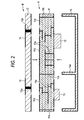
- Fig. 2 is a sectional view in which the electronic component module of Fig. 1 is disassembled into constituent elements.
- Fig. 3 is a sectional view of an electronic component module according to another embodiment of the invention.
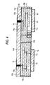
- Fig. 4 is a sectional view of an electronic component module according to still another embodiment of the invention.
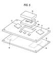
- Fig. 5 is an exploded perspective view of an electronic component module according to a further embodiment of the invention.
-
- The best mode for carrying out the invention will be hereinafter described in detail with reference to the drawings. In the accompanying drawings, the same members are given the same reference symbol. And redundant descriptions will be omitted. The following descriptions will be directed to the best mode for carrying out the invention, and hence the invention is not limited to it.
- As shown in Fig. 1, an
electronic component module 10 according to this embodiment is equipped with a firstdielectric substrate 11 that has a lamination structure and is made of a ceramic dielectric such as LTCC (low temperature co-fired ceramics) and a seconddielectric substrate 12 that is made of a resin dielectric such as a fluororesin, a BT resin, a PPE(O) resin, or a graft polymerization resin and is laid on the first dielectric substrate 11 (i.e., thesubstrates dielectric substrate 11 and the seconddielectric substrate 12 constitute a device-side module A and an antenna-side module B, respectively. -
First transmission lines 11a are formed in layers in the firstdielectric substrate 11, andsecond transmission lines 12a are formed in the seconddielectric substrate 12. Thefirst transmission lines 11a and thesecond transmission lines 12a are composed of a waveguide and a conductor (in a through-hole) and are made of Au, Ag, Cu, W, or the like. As shown in Fig. 1, thefirst transmission lines 11a and thesecond transmission lines 12a are electrically connected to each other. High-frequency devices 13 are mounted on the firstdielectric substrate 11 and connected to thefirst transmission lines 11a, andantenna elements 14 such as patch antennas are provided on the seconddielectric substrate 12 and connected to thesecond transmission lines 12a. Therefore, theantenna elements 14 send or receive a signal to or from the high-frequency devices 13 via thesecond transmission lines 12a and thefirst transmission lines 11a that are connected to each other directly. - The high-
frequency devices 13 are electronic components that are used in, for example, a 25 GHz band that is a sub-millimeter wave band or a 5 GHz band that is a microwave band. The high-frequency devices 13 are mounted on the firstdielectric substrate 11 by surface mounting by soldering or brazing or flip chip mounting with Au, an Au-Sn alloy, or the like. Examples of the high-frequency device 13 are a power amplifier, a mixer, amultiplier, a frequency converter, a high-frequency oscillator, and a low-noise power amplifier. However, the high-frequency devices 13 are not limited to these electronic components. A plurality ofantenna elements 14 are formed in array form to obtain good directivity. - A
ground layer 11d that is formed on the firstdielectric substrate 11 andconductive layers 11b that are connected to theground layer 11d and extend in the lamination direction also serve as shield layers (described later). - The material of the first
dielectric substrate 11 and the seconddielectric substrate 12 is not limited to ceramics or a resin and may be another dielectric material. However, the firstdielectric substrate 11 made of ceramics makes it possible to mount the high-frequency devices 13 by thermocompression bonding at about 400°C as in the case of Au connection. The firstdielectric substrate 11 need not have a lamination structure. However, the employment of a lamination structure as in this embodiment facilitates formation of a filter functional component etc. within a substrate. The seconddielectric substrate 12 made of a resin having low dielectric constant makes it possible to increase the antenna efficiency. It is desirable that the relative dielectric constants of the firstdielectric substrate 11 and the seconddielectric substrate 12 be about 6 to 45 and about 2 to 5, respectively. - Alternatively, a single,
unarrayed antenna element 14 may be employed, an example of which is a multi-band antenna capable of sending and receiving radio waves of a plurality of frequencies by a single antenna. Further, theantenna element 14 is not limited to a patch antenna that is employed in this embodiment and may be any of other forms of antenna such as an inverted-F antenna and a slot antenna. - The first
dielectric substrate 11 is equipped with a shielding means for electromagnetically shielding the high-frequency devices 13 by surrounding those. The shielding means is composed of the above-mentioned shield layers (i.e., theconductive layers 11b and theground layer 11d that are formed in or on the first dielectric substrate 11) and alid member 15 that seals the high-frequency devices 13. Thelid member 15, which is given a shield function in such a manner that, for example, a resin is plated with a metal, electromagnetically seals the high-frequency devices 13 together with the shield layers. Alternatively, thelid member 15 itself may be made of a metal so as to be given a shield function. In the illustrated example, thelid member 15 is formed with apartition 15a and electromagnetically seals the high-frequency devices 13 individually together with theconductive layers 11b formed in the firstdielectric substrate 11. As such, thelid member 15 prevents even electromagnetic interference between the high-frequency devices 13: stable operating characteristics are obtained by an improved isolation characteristic. Alternatively, thepartition 15a may be omitted in which case only electromagnetic shielding from the outside is attained. - As described above, in the
electronic component module 10 according to this embodiment, thefirst transmission lines 11a formed in the firstdielectric substrate 11 that is mounted with the high-frequency devices 13 and thesecond transmission lines 12a formed in the seconddielectric substrate 12 that is provided with theantenna elements 14 are directly connected to each other electrically. Therefore, unlike in the case that thefirst transmission lines 11a and thesecond transmission lines 12a are connected to each other electromagnetically via slots, the physical dimensions of the module are not dominated by a frequency used or the signal pass frequency band is not restricted by the dimension of slots. This makes it possible to miniaturize and increase the bandwidth of the antenna-integrated electronic component module. - Further, since the high-
frequency devices 13 are electromagnetically shielded by the shielding means, electromagnetic influences from external electronic apparatus are prevented and hence the operation can be stabilized. Still further, since the high-frequency devices 13 are electromagnetically shielded individually, undesirable electromagnetic coupling in the electronic component module is prevented and the isolation characteristic between the devices is improved, whereby the operating characteristics can be made even more stable. - Next, a manufacturing method of the above-configured electronic component module will be described.
- First, the high-
frequency devices 13 are mounted on the mounting surface of the firstdielectric substrate 11 so as to be connected to thefirst transmission lines 11a, whereby the device-side module A is formed. And theantenna elements 14 are provided on the seconddielectric substrate 12 so as to be connected to thesecond transmission lines 12a, whereby the antenna-side module B is formed (see Fig. 2). Then, the firstdielectric substrate 11 and the seconddielectric substrate 12 are joined to each other in the lamination direction, whereby thefirst transmission lines 11a and thesecond transmission lines 12a are electrically connected to each other. - As a result, the high-
frequency devices 13 and theantenna elements 14 are connected to each other via thefirst transmission lines 11a and thesecond transmission lines 12a that are directly connected to the high-frequency devices 13 and theantenna elements 14, respectively. Therefore, as described above, the antenna-integrated electronic component module can be miniaturized and increased in bandwidth. - This manufacturing method makes it possible to construct an antenna-integrated electronic component module in which the first
dielectric substrate 11 and the seconddielectric substrate 12 are in such a combination that they cannot be fired simultaneously as in the combination of this embodiment that the firstdielectric substrate 11 and the seconddielectric substrate 12 are made of ceramics and a resin, respectively. - The joining of the first
dielectric substrate 11 and the seconddielectric substrate 12 is performed in the following manner. First, a solder layer as a conductive bonding member is formed on one or both of portions of thefirst transmission lines 11a that are exposed in the surface, to be bonded to the seconddielectric substrate 12, of the firstdielectric substrate 11 and portions of thesecond transmission lines 12a that are exposed in the surface, to be bonded to the firstdielectric substrate 11, of the seconddielectric substrate 12. The solder layer may be in any of paste form, sheet form, ball form, and BGA (ball grid array) form. - Materials other than solder may be used as the conductive bonding member. For example, paste or sheet-like conductive resins containing a metal that are set when heat, light, an electron beam, or moisture is applied to them may be used.
- After application of the solder, the
first transmission lines 11a and thesecond transmission lines 12a are aligned with respect to each other and the firstdielectric substrate 11 and the seconddielectric substrate 12 are laid on each other and heated. As a result, the solder layer is melted and thefirst transmission lines 11a and thesecond transmission lines 12a are joined to each other. - Although molten solder extends across the exposed portions of the
first transmission lines 11a and thesecond transmission lines 12a having small contact angles, it does not extend to the other regions having large contact angles. Therefore, the firstdielectric substrate 11 and the seconddielectric substrate 12 are positioned by the surface tension of the solder in such a manner that thefirst transmission lines 11a and thesecond transmission lines 12a face each other correctly. - Finally, after the positioning, the joined structure is left at ordinary temperature and the solder solidifies: the first
dielectric substrate 11 and the seconddielectric substrate 12 are fixed to each other while being positioned correctly. In this manner, the twosubstrates first transmission lines 11a and thesecond transmission lines 12a, which requires fine alignment, can be performed correctly. - After the joining of the first
dielectric substrate 11 and the seconddielectric substrate 12, thelid member 15 is attached to the firstdielectric substrate 11 to shield the high-frequency devices 13 electromagnetically (see Fig.2). Theelectronic component module 10 is thus completed. - The invention is not limited to the above embodiment. For example, as shown in Fig. 3, the
lid member 15 may be composed of a plate-like lid 15b andspacers 15c as side walls. - As shown in Fig. 4, a configuration is possible in which
cavities 11b are formed in the firstdielectric substrate 11 and the high-frequency devices 13 are mounted in thecavities 11b. This configuration can reduce the height and the loss of theelectronic component module 10. - Further, an electronic component module may be constructed as shown in Fig. 5. A third
dielectric substrate 16 that is formed with a through-hole 16a in which the firstdielectric substrate 11 mounted with the high-frequency devices 13 is inserted and that is mounted with low-frequencyfunctional components 17. The thirddielectric substrate 16 is fixed to the seconddielectric substrate 12 by screwing, for example, whereby the firstdielectric substrate 11 and the seconddielectric substrate 12 are aligned with each other. The firstdielectric substrate 11 and the thirddielectric substrate 16 are electrically connected to each other via bonded wires, gold ribbons, a cable and connectors, or the like. - Examples of the low-frequency functional components are a control circuit, a computing circuit, and a signal processing circuit. However, the low-frequency functional components are not limited to these electronic components.
- An inexpensive electronic component module can be constructed by using, as the third
dielectric substrate 16, a common resin substrate such as a glass epoxy resin substrate.
Claims (14)
- An electronic component module characterized by comprising:a device-side module comprising:a first dielectric substrate that is formed with a first transmission line; anda high-frequency device that is mounted on the first dielectric substrate and connected to the first transmission line; andan antenna-side module comprising:a second dielectric substrate that is laid on the first dielectric substrate in such a manner that they are arranged in a lamination direction and that is formed with a second transmission line that is electrically connected to the first transmission line; andan antenna element that is provided on the second dielectric substrate and electrically connected to the high-frequency device via the second transmission line and the first transmission line.
- The electronic component module according to claim 1, further comprising a third dielectric substrate that is formed with a through-hole in which the first dielectric substrate is inserted, mounted with a low-frequency functional component, fixed to the second dielectric substrate, and electrically connected to the first dielectric substrate.
- The electronic component module according to claim 1, wherein the first dielectric substrate is made of ceramics.
- The electronic component module according to claim 3, wherein the first dielectric substrate is made of low temperature co-fired ceramics.
- The electronic component module according to claim 1, wherein the second dielectric substrate is made of a resin.
- The electronic component module according to claim 1, wherein the first dielectric substrate is formed with a cavity and the high-frequency device is mounted in the cavity.
- The electronic component module according to claim 1, wherein the first dielectric substrate is provided with shielding means that surrounds the high-frequency device and thereby shields it electromagnetically.
- The electronic component module according to claim 7, wherein the shielding means electromagnetically shields a plurality of high-frequency devices individually.
- The electronic component module according to claim 8, wherein the shielding means comprises a shield layer that is formed in the first dielectric substrate and a lid member that seals the high-frequency devices.
- The electronic component module according to claim 1, wherein the first dielectric substrate and the second dielectric substrate are laminated on each other.
- Amanufacturing method of an electronic component module, comprising the steps of:forming a device-side module by mounting a high-frequency device on a first dielectric substrate in such a manner that the high-frequency device is connected to a first transmission line;forming an antenna-side module by providing an antenna element on a second dielectric substrate in such a manner that the antenna element is connected to a second transmission line; andjoining the first dielectric substrate and the second dielectric substrate to each other in a lamination direction and thereby electrically connecting the first transmission line and the second transmission line to each other.
- The manufacturing method of an electronic component module according to claim 11, wherein the joining of the first dielectric substrate and the second dielectric substrate is performed by:applying a conductive bonding material to at least one of a portion of the first transmission line that is exposed in a surface, to be joined to the second dielectric substrate, of the first dielectric substrate and a portion of the second transmission line that is exposed in a surface, to be joined to the first dielectric substrate, of the second dielectric substrate;aligning the first transmission line and the second transmission line with each other and laying the first dielectric substrate and the second dielectric substrate on each other; andsolidifying the conductive bonding material and thereby fixing the first transmission line and the second transmission line to each other with electrical continuity established between them.
- The manufacturing method of an electronic component module according to claim 12, wherein the conductive bonding material is solder.
- The manufacturing method of an electronic component module according to claim 12, wherein the conductive bonding material is a conductive resin containing a metal.
Applications Claiming Priority (2)
| Application Number | Priority Date | Filing Date | Title |
|---|---|---|---|
| JP2003317757 | 2003-09-10 | ||
| JP2003317757A JP2005086603A (en) | 2003-09-10 | 2003-09-10 | Electronic component module and manufacturing method thereof |
Publications (2)
| Publication Number | Publication Date |
|---|---|
| EP1515389A1 true EP1515389A1 (en) | 2005-03-16 |
| EP1515389B1 EP1515389B1 (en) | 2006-11-15 |
Family
ID=34131988
Family Applications (1)
| Application Number | Title | Priority Date | Filing Date |
|---|---|---|---|
| EP04021051A Expired - Lifetime EP1515389B1 (en) | 2003-09-10 | 2004-09-03 | Multilayer high frequency device with planar antenna thereon and manufacturing method thereof |
Country Status (5)
| Country | Link |
|---|---|
| US (1) | US7236070B2 (en) |
| EP (1) | EP1515389B1 (en) |
| JP (1) | JP2005086603A (en) |
| CN (1) | CN1595649A (en) |
| DE (1) | DE602004003191T2 (en) |
Cited By (5)
| Publication number | Priority date | Publication date | Assignee | Title |
|---|---|---|---|---|
| EP1750370A3 (en) * | 2005-08-01 | 2008-09-17 | Samsung Electronics Co.,Ltd. | Monolithic duplexer and fabrication method thereof |
| WO2008121723A1 (en) | 2007-03-29 | 2008-10-09 | Intel Corporation | Multi-band highly isolated planar antennas integrated with front-end modules for mobile applications |
| EP2068393A1 (en) * | 2007-12-07 | 2009-06-10 | Panasonic Corporation | Laminated RF device with vertical resonators |
| WO2011094539A1 (en) * | 2010-01-29 | 2011-08-04 | E. I. Du Pont De Nemours And Company | Method of manufacturing high frequency receiving and/or transmitting devices from low temperature co fired ceramic materials and devices made therefrom |
| EP3043382A1 (en) * | 2015-01-07 | 2016-07-13 | Delphi Technologies, Inc. | Circuit board assembly with high and low frequency substrates |
Families Citing this family (82)
| Publication number | Priority date | Publication date | Assignee | Title |
|---|---|---|---|---|
| JP3973402B2 (en) * | 2001-10-25 | 2007-09-12 | 株式会社日立製作所 | High frequency circuit module |
| CN1774965A (en) * | 2004-03-30 | 2006-05-17 | 松下电器产业株式会社 | Module component and method for manufacturing the same |
| JP4749795B2 (en) * | 2005-08-05 | 2011-08-17 | 新光電気工業株式会社 | Semiconductor device |
| JP4721270B2 (en) * | 2005-08-24 | 2011-07-13 | 日本無線株式会社 | Antenna manufacturing method |
| WO2007049376A1 (en) * | 2005-10-27 | 2007-05-03 | Murata Manufacturing Co., Ltd. | High-frequency module |
| JP4620576B2 (en) * | 2005-12-02 | 2011-01-26 | パナソニック株式会社 | Wireless device |
| JP4656235B2 (en) * | 2006-04-28 | 2011-03-23 | パナソニック株式会社 | Manufacturing method of electronic circuit module with built-in antenna |
| JP4730196B2 (en) * | 2006-05-08 | 2011-07-20 | パナソニック株式会社 | Card type information device |
| JP2007306172A (en) * | 2006-05-10 | 2007-11-22 | Tdk Corp | Bandpass filter element, and high frequency module |
| JP5123493B2 (en) * | 2006-05-30 | 2013-01-23 | 新光電気工業株式会社 | Wiring substrate and semiconductor device |
| US8171191B2 (en) * | 2006-08-04 | 2012-05-01 | Arm Limited | Bus interconnect device and a data processing apparatus including such a bus interconnect device |
| US7477197B2 (en) * | 2006-12-29 | 2009-01-13 | Intel Corporation | Package level integration of antenna and RF front-end module |
| JP2008205067A (en) * | 2007-02-19 | 2008-09-04 | Sharp Corp | High frequency signal processing module and electronic device |
| US7573359B2 (en) * | 2007-03-29 | 2009-08-11 | Intel Corporation | Reducing crosstalk in electronic devices having microstrip lines covered by a flexible insulating material and a metallic backing plate |
| JP4996345B2 (en) * | 2007-05-30 | 2012-08-08 | 株式会社東芝 | Antenna device and information terminal device |
| US7852270B2 (en) * | 2007-09-07 | 2010-12-14 | Sharp Kabushiki Kaisha | Wireless communication device |
| US7855685B2 (en) * | 2007-09-28 | 2010-12-21 | Delphi Technologies, Inc. | Microwave communication package |
| US9007265B2 (en) * | 2009-01-02 | 2015-04-14 | Polytechnic Institute Of New York University | Using dielectric substrates, embedded with vertical wire structures, with slotline and microstrip elements to eliminate parallel-plate or surface-wave radiation in printed-circuits, chip packages and antennas |
| JP2011216957A (en) * | 2010-03-31 | 2011-10-27 | Furukawa Electric Co Ltd:The | High-frequency circuit board |
| US20120170230A1 (en) * | 2010-12-30 | 2012-07-05 | Research In Motion Limited | Combining printed circuit boards |
| DE102011005145A1 (en) * | 2011-03-04 | 2012-09-06 | Rohde & Schwarz Gmbh & Co. Kg | Circuit board assembly for millimeter wave scanner |
| US9780928B2 (en) | 2011-10-17 | 2017-10-03 | Golba Llc | Method and system for providing diversity in a network that utilizes distributed transceivers and array processing |
| US9166284B2 (en) * | 2012-12-20 | 2015-10-20 | Intel Corporation | Package structures including discrete antennas assembled on a device |
| US9172131B2 (en) * | 2013-03-15 | 2015-10-27 | Advanced Semiconductor Engineering, Inc. | Semiconductor structure having aperture antenna |
| JP5756500B2 (en) * | 2013-08-07 | 2015-07-29 | 太陽誘電株式会社 | Circuit module |
| WO2016120254A1 (en) * | 2015-01-27 | 2016-08-04 | At & S Austria Technologie & Systemtechnik Aktiengesellschaft | Component carrier with integrated antenna structure |
| US11335651B2 (en) * | 2015-12-22 | 2022-05-17 | Intel Corporation | Microelectronic devices designed with compound semiconductor devices and integrated on an inter die fabric |
| JP2017183653A (en) * | 2016-03-31 | 2017-10-05 | スナップトラック・インコーポレーテッド | Multi-layer wiring board for high frequency and its manufacturing method |
| CN107369673B (en) * | 2016-05-13 | 2019-11-05 | 华为技术有限公司 | It is provided with the integrated circuit package device and its manufacturing method of antenna |
| US10854995B2 (en) | 2016-09-02 | 2020-12-01 | Movandi Corporation | Wireless transceiver having receive antennas and transmit antennas with orthogonal polarizations in a phased array antenna panel |
| FR3055742B1 (en) * | 2016-09-06 | 2019-12-20 | Commissariat A L'energie Atomique Et Aux Energies Alternatives | MILLIMETER WAVE GUIDE |
| WO2018074553A1 (en) * | 2016-10-21 | 2018-04-26 | 京セラ株式会社 | Substrate for tags, rfid tag and rfid system |
| US10199717B2 (en) | 2016-11-18 | 2019-02-05 | Movandi Corporation | Phased array antenna panel having reduced passive loss of received signals |
| US10594019B2 (en) | 2016-12-03 | 2020-03-17 | International Business Machines Corporation | Wireless communications package with integrated antenna array |
| US10396432B2 (en) * | 2017-01-23 | 2019-08-27 | Samsung Electro-Mechanics Co., Ltd. | Antenna-integrated radio frequency module |
| WO2018186065A1 (en) * | 2017-04-03 | 2018-10-11 | 株式会社村田製作所 | High frequency module |
| TWI678772B (en) * | 2017-04-28 | 2019-12-01 | 矽品精密工業股份有限公司 | Electronic package and method for fabricating the same |
| TWI663701B (en) * | 2017-04-28 | 2019-06-21 | Siliconware Precision Industries Co., Ltd. | Electronic package and method for fabricating the same |
| WO2018203640A1 (en) * | 2017-05-02 | 2018-11-08 | 주식회사 아모텍 | Antenna module |
| US10916861B2 (en) * | 2017-05-30 | 2021-02-09 | Movandi Corporation | Three-dimensional antenna array module |
| US10321332B2 (en) | 2017-05-30 | 2019-06-11 | Movandi Corporation | Non-line-of-sight (NLOS) coverage for millimeter wave communication |
| CN110710118B (en) * | 2017-06-02 | 2021-08-20 | 株式会社村田制作所 | High frequency module and communication device |
| US10484078B2 (en) | 2017-07-11 | 2019-11-19 | Movandi Corporation | Reconfigurable and modular active repeater device |
| US12368497B2 (en) | 2017-07-11 | 2025-07-22 | Movandi Corporation | Repeater device for 5G new radio communication |
| US10658762B2 (en) | 2017-07-14 | 2020-05-19 | Apple Inc. | Multi-band millimeter wave antenna arrays |
| US10971825B2 (en) * | 2017-07-28 | 2021-04-06 | Samsung Electro-Mechanics Co., Ltd. | Antenna module and method of manufacturing the same |
| US11095037B2 (en) | 2017-08-11 | 2021-08-17 | Samsung Electro-Mechanics Co., Ltd. | Antenna module |
| JP6905438B2 (en) * | 2017-09-22 | 2021-07-21 | 株式会社フジクラ | Wireless communication module |
| JP6946890B2 (en) * | 2017-09-22 | 2021-10-13 | Tdk株式会社 | Composite electronic components |
| KR102494338B1 (en) * | 2017-11-08 | 2023-02-01 | 삼성전기주식회사 | Antenna module |
| KR102410799B1 (en) * | 2017-11-28 | 2022-06-21 | 삼성전자주식회사 | Antenna system for transmitting and receiving mm-wave signal |
| JP7023683B2 (en) | 2017-11-29 | 2022-02-22 | Tdk株式会社 | Patch antenna |
| US10348371B2 (en) | 2017-12-07 | 2019-07-09 | Movandi Corporation | Optimized multi-beam antenna array network with an extended radio frequency range |
| US10090887B1 (en) | 2017-12-08 | 2018-10-02 | Movandi Corporation | Controlled power transmission in radio frequency (RF) device network |
| US10862559B2 (en) | 2017-12-08 | 2020-12-08 | Movandi Corporation | Signal cancellation in radio frequency (RF) device network |
| KR102022353B1 (en) * | 2018-01-18 | 2019-09-18 | 삼성전기주식회사 | Antenna module |
| US10637159B2 (en) | 2018-02-26 | 2020-04-28 | Movandi Corporation | Waveguide antenna element-based beam forming phased array antenna system for millimeter wave communication |
| US11088457B2 (en) | 2018-02-26 | 2021-08-10 | Silicon Valley Bank | Waveguide antenna element based beam forming phased array antenna system for millimeter wave communication |
| KR102003840B1 (en) | 2018-03-12 | 2019-07-25 | 삼성전자주식회사 | Antenna module |
| KR102520212B1 (en) * | 2018-04-05 | 2023-04-10 | 삼성전기주식회사 | Electronic component module and manufacturing mehthod therof |
| KR102518174B1 (en) * | 2018-04-05 | 2023-04-05 | 삼성전기주식회사 | Electronic component module |
| US10564679B2 (en) * | 2018-04-05 | 2020-02-18 | Samsung Electro-Mechanics Co., Ltd. | Electronic device module, method of manufacturing the same and electronic apparatus |
| CN110828962B (en) | 2018-08-09 | 2021-08-03 | 财团法人工业技术研究院 | Antenna array module and manufacturing method thereof |
| JP7091961B2 (en) * | 2018-09-13 | 2022-06-28 | Tdk株式会社 | On-chip antenna |
| EP3734764B1 (en) * | 2018-10-18 | 2023-11-08 | Amotech Co., Ltd. | Antenna package having cavity structure |
| US11205855B2 (en) | 2018-12-26 | 2021-12-21 | Silicon Valley Bank | Lens-enhanced communication device |
| US11145986B2 (en) | 2018-12-26 | 2021-10-12 | Silicon Valley Bank | Lens-enhanced communication device |
| JP7021718B2 (en) * | 2019-03-25 | 2022-02-17 | 株式会社村田製作所 | Filters, antenna modules and communication devices |
| US11043740B2 (en) * | 2019-05-14 | 2021-06-22 | Qualcomm Incorporated | Enhanced antenna module with shield layer |
| KR102533885B1 (en) * | 2019-05-31 | 2023-05-18 | 가부시키가이샤 무라타 세이사쿠쇼 | Sub-array antenna, array antenna, antenna module and communication device |
| US20210045227A1 (en) * | 2019-08-08 | 2021-02-11 | At&S Austria Technologie & Systemtechnik Aktiengesellschaft | Component Carrier, Method of Manufacturing the Same and Method of Shielding a Structural Feature in a Component Carrier |
| KR102257930B1 (en) * | 2019-08-13 | 2021-05-28 | 삼성전기주식회사 | Chip antenna |
| JP7295971B2 (en) * | 2019-11-26 | 2023-06-21 | 京セラ株式会社 | antenna module |
| KR102731798B1 (en) * | 2019-12-10 | 2024-11-19 | 삼성전기주식회사 | Antenna substrate and antenna module comprising the same |
| KR102723705B1 (en) * | 2020-07-08 | 2024-10-29 | 삼성전기주식회사 | Antenna apparatus |
| JP7516139B2 (en) * | 2020-07-13 | 2024-07-16 | 古河電気工業株式会社 | Antenna Module |
| US11557544B2 (en) * | 2020-08-27 | 2023-01-17 | Nxp Usa, Inc. | Semiconductor device having a translation feature and method therefor |
| US11901270B2 (en) | 2020-09-02 | 2024-02-13 | Advanced Semiconductor Engineering, Inc. | Semiconductor device package |
| KR102517347B1 (en) * | 2021-04-29 | 2023-04-03 | 주식회사 엘지유플러스 | Broadband antenna module and mobile terminal having the same |
| JP7665501B2 (en) * | 2021-11-19 | 2025-04-21 | 京セラ株式会社 | Antenna Device |
| AU2021480187A1 (en) | 2021-12-22 | 2024-07-11 | Viasat, Inc. | Antenna apparatus employing radiation shield for integrated circuits |
| US12451589B2 (en) * | 2023-02-21 | 2025-10-21 | Tron Future Tech Inc. | Antenna package and method for manufacturing an antenna package |
Citations (5)
| Publication number | Priority date | Publication date | Assignee | Title |
|---|---|---|---|---|
| EP0198698B1 (en) * | 1985-04-13 | 1991-10-23 | Fujitsu Limited | Integrated circuit device having strip line structure therein |
| FR2710195A1 (en) * | 1993-09-14 | 1995-03-24 | Thomson Csf | Antenna-electronic circuit assembly |
| JPH09237867A (en) * | 1996-02-29 | 1997-09-09 | Kyocera Corp | High frequency package |
| WO1999062135A1 (en) * | 1998-05-26 | 1999-12-02 | Circuit Components Incorporated | Wideband rf port structure using coplanar waveguide and bga i/o |
| EP1307078A2 (en) * | 2001-10-25 | 2003-05-02 | Hitachi, Ltd. | High frequency circuit module |
Family Cites Families (24)
| Publication number | Priority date | Publication date | Assignee | Title |
|---|---|---|---|---|
| JP2580604B2 (en) * | 1987-06-19 | 1997-02-12 | 三菱電機株式会社 | Microwave integrated circuit with integrated antenna |
| JP2606044B2 (en) * | 1991-04-24 | 1997-04-30 | 松下電器産業株式会社 | Dielectric filter |
| US5768109A (en) * | 1991-06-26 | 1998-06-16 | Hughes Electronics | Multi-layer circuit board and semiconductor flip chip connection |
| JP2840493B2 (en) * | 1991-12-27 | 1998-12-24 | 株式会社日立製作所 | Integrated microwave circuit |
| JPH07170115A (en) * | 1993-12-15 | 1995-07-04 | Fujitsu Ten Ltd | High frequency circuit with tri-plate antenna |
| JPH0964636A (en) * | 1995-08-21 | 1997-03-07 | Matsushita Electric Ind Co Ltd | Planar antenna |
| JP3427040B2 (en) * | 1996-02-29 | 2003-07-14 | 京セラ株式会社 | High frequency package |
| JPH1027987A (en) * | 1996-07-10 | 1998-01-27 | Hitachi Ltd | Low EMI circuit board and low EMI cable connector |
| JPH10224120A (en) * | 1997-02-06 | 1998-08-21 | Murata Mfg Co Ltd | Dielectric line |
| JPH10303640A (en) * | 1997-04-25 | 1998-11-13 | Nippon Telegr & Teleph Corp <Ntt> | Antenna device |
| US6515562B1 (en) * | 1998-04-23 | 2003-02-04 | Kyocera Corporation | Connection structure for overlapping dielectric waveguide lines |
| JP3129288B2 (en) * | 1998-05-28 | 2001-01-29 | 日本電気株式会社 | Microwave integrated circuit multi-chip module, mounting structure of microwave integrated circuit multi-chip module |
| JP3331967B2 (en) | 1998-06-02 | 2002-10-07 | 松下電器産業株式会社 | Millimeter wave module |
| JP2000216630A (en) * | 1999-01-20 | 2000-08-04 | Alps Electric Co Ltd | Transmitter-receiver with antenna |
| JP3687443B2 (en) * | 1999-10-12 | 2005-08-24 | 株式会社村田製作所 | Low temperature fired ceramic composition and ceramic multilayer substrate |
| US6456172B1 (en) * | 1999-10-21 | 2002-09-24 | Matsushita Electric Industrial Co., Ltd. | Multilayered ceramic RF device |
| CN1543298A (en) * | 2000-06-27 | 2004-11-03 | ���µ�����ҵ��ʽ���� | Ceramic laminated device |
| JP2002164733A (en) * | 2000-11-24 | 2002-06-07 | Sony Corp | Planar antenna device |
| JP3941416B2 (en) * | 2001-04-26 | 2007-07-04 | ソニー株式会社 | High frequency module device and manufacturing method thereof |
| US6784759B2 (en) * | 2001-07-27 | 2004-08-31 | Matsushita Electric Industrial Co., Ltd. | Antenna duplexer and communication apparatus |
| JP2003204211A (en) * | 2002-09-30 | 2003-07-18 | Nec Corp | Microwave/millimeter wave circuit device |
| JP2004327641A (en) * | 2003-04-24 | 2004-11-18 | Tdk Corp | Electronic component module |
| JP2004342948A (en) * | 2003-05-19 | 2004-12-02 | Tdk Corp | Electronic component module |
| JP3734807B2 (en) * | 2003-05-19 | 2006-01-11 | Tdk株式会社 | Electronic component module |
-
2003
- 2003-09-10 JP JP2003317757A patent/JP2005086603A/en active Pending
-
2004
- 2004-08-30 US US10/928,244 patent/US7236070B2/en not_active Expired - Lifetime
- 2004-09-03 EP EP04021051A patent/EP1515389B1/en not_active Expired - Lifetime
- 2004-09-03 DE DE602004003191T patent/DE602004003191T2/en not_active Expired - Lifetime
- 2004-09-10 CN CNA2004100770934A patent/CN1595649A/en active Pending
Patent Citations (5)
| Publication number | Priority date | Publication date | Assignee | Title |
|---|---|---|---|---|
| EP0198698B1 (en) * | 1985-04-13 | 1991-10-23 | Fujitsu Limited | Integrated circuit device having strip line structure therein |
| FR2710195A1 (en) * | 1993-09-14 | 1995-03-24 | Thomson Csf | Antenna-electronic circuit assembly |
| JPH09237867A (en) * | 1996-02-29 | 1997-09-09 | Kyocera Corp | High frequency package |
| WO1999062135A1 (en) * | 1998-05-26 | 1999-12-02 | Circuit Components Incorporated | Wideband rf port structure using coplanar waveguide and bga i/o |
| EP1307078A2 (en) * | 2001-10-25 | 2003-05-02 | Hitachi, Ltd. | High frequency circuit module |
Cited By (8)
| Publication number | Priority date | Publication date | Assignee | Title |
|---|---|---|---|---|
| EP1750370A3 (en) * | 2005-08-01 | 2008-09-17 | Samsung Electronics Co.,Ltd. | Monolithic duplexer and fabrication method thereof |
| WO2008121723A1 (en) | 2007-03-29 | 2008-10-09 | Intel Corporation | Multi-band highly isolated planar antennas integrated with front-end modules for mobile applications |
| EP2137793A4 (en) * | 2007-03-29 | 2011-04-13 | Intel Corp | Multi-band highly isolated planar antennas integrated with front-end modules for mobile applications |
| US8077095B2 (en) | 2007-03-29 | 2011-12-13 | Intel Corporation | Multi-band highly isolated planar antennas integrated with front-end modules for mobile applications |
| EP2068393A1 (en) * | 2007-12-07 | 2009-06-10 | Panasonic Corporation | Laminated RF device with vertical resonators |
| WO2011094539A1 (en) * | 2010-01-29 | 2011-08-04 | E. I. Du Pont De Nemours And Company | Method of manufacturing high frequency receiving and/or transmitting devices from low temperature co fired ceramic materials and devices made therefrom |
| US8633858B2 (en) | 2010-01-29 | 2014-01-21 | E I Du Pont De Nemours And Company | Method of manufacturing high frequency receiving and/or transmitting devices from low temperature co-fired ceramic materials and devices made therefrom |
| EP3043382A1 (en) * | 2015-01-07 | 2016-07-13 | Delphi Technologies, Inc. | Circuit board assembly with high and low frequency substrates |
Also Published As
| Publication number | Publication date |
|---|---|
| DE602004003191T2 (en) | 2007-02-22 |
| US7236070B2 (en) | 2007-06-26 |
| EP1515389B1 (en) | 2006-11-15 |
| US20050088260A1 (en) | 2005-04-28 |
| CN1595649A (en) | 2005-03-16 |
| DE602004003191D1 (en) | 2006-12-28 |
| JP2005086603A (en) | 2005-03-31 |
Similar Documents
| Publication | Publication Date | Title |
|---|---|---|
| US7236070B2 (en) | Electronic component module and manufacturing method thereof | |
| JP4786579B2 (en) | High frequency module | |
| US12074124B2 (en) | Integrated circuit package with integrated waveguide launcher | |
| US6788171B2 (en) | Millimeter wave (MMW) radio frequency transceiver module and method of forming same | |
| US7239222B2 (en) | High frequency circuit module | |
| EP0766410B1 (en) | Ultra high frequency radio communication apparatus | |
| US6556169B1 (en) | High frequency circuit integrated-type antenna component | |
| CN112970146B (en) | Wiring substrate, antenna module, and communication device | |
| JP2004327641A (en) | Electronic component module | |
| US6483406B1 (en) | High-frequency module using slot coupling | |
| CN103703610B (en) | Wireless module | |
| EP2449621B1 (en) | Hybrid single aperture inclined antenna | |
| WO2000035015A1 (en) | Rf circuit module | |
| KR100713195B1 (en) | High frequency module and method of manufacturing the same | |
| JP3969321B2 (en) | High frequency transmitter / receiver module | |
| JP3631667B2 (en) | Wiring board and its connection structure with waveguide | |
| JP2580604B2 (en) | Microwave integrated circuit with integrated antenna | |
| KR20200120464A (en) | Chip antenna module | |
| JP2004342948A (en) | Electronic component module | |
| JPH1117063A (en) | Circuit board for mounting semiconductor chip, package for storing semiconductor chip, and semiconductor device | |
| JP2798070B2 (en) | Composite microwave integrated circuit | |
| JP2004297465A (en) | High frequency package | |
| JP3140385B2 (en) | High frequency semiconductor device | |
| JP2001088097A (en) | Millimeter-wave multilayer substrate module and method of manufacturing the same | |
| JP3071761B2 (en) | Mounting structure of high frequency semiconductor device |
Legal Events
| Date | Code | Title | Description |
|---|---|---|---|
| PUAI | Public reference made under article 153(3) epc to a published international application that has entered the european phase |
Free format text: ORIGINAL CODE: 0009012 |
|
| AK | Designated contracting states |
Kind code of ref document: A1 Designated state(s): AT BE BG CH CY CZ DE DK EE ES FI FR GB GR HU IE IT LI LU MC NL PL PT RO SE SI SK TR |
|
| AX | Request for extension of the european patent |
Extension state: AL HR LT LV MK |
|
| 17P | Request for examination filed |
Effective date: 20050517 |
|
| 17Q | First examination report despatched |
Effective date: 20050617 |
|
| AKX | Designation fees paid |
Designated state(s): DE FR GB IT SE |
|
| GRAP | Despatch of communication of intention to grant a patent |
Free format text: ORIGINAL CODE: EPIDOSNIGR1 |
|
| GRAS | Grant fee paid |
Free format text: ORIGINAL CODE: EPIDOSNIGR3 |
|
| GRAA | (expected) grant |
Free format text: ORIGINAL CODE: 0009210 |
|
| AK | Designated contracting states |
Kind code of ref document: B1 Designated state(s): DE FR GB IT SE |
|
| REG | Reference to a national code |
Ref country code: GB Ref legal event code: FG4D |
|
| REF | Corresponds to: |
Ref document number: 602004003191 Country of ref document: DE Date of ref document: 20061228 Kind code of ref document: P |
|
| REG | Reference to a national code |
Ref country code: SE Ref legal event code: TRGR |
|
| ET | Fr: translation filed | ||
| PLBE | No opposition filed within time limit |
Free format text: ORIGINAL CODE: 0009261 |
|
| STAA | Information on the status of an ep patent application or granted ep patent |
Free format text: STATUS: NO OPPOSITION FILED WITHIN TIME LIMIT |
|
| 26N | No opposition filed |
Effective date: 20070817 |
|
| PGFP | Annual fee paid to national office [announced via postgrant information from national office to epo] |
Ref country code: GB Payment date: 20090902 Year of fee payment: 6 Ref country code: SE Payment date: 20090910 Year of fee payment: 6 |
|
| PGFP | Annual fee paid to national office [announced via postgrant information from national office to epo] |
Ref country code: FR Payment date: 20091012 Year of fee payment: 6 Ref country code: IT Payment date: 20090912 Year of fee payment: 6 |
|
| PGFP | Annual fee paid to national office [announced via postgrant information from national office to epo] |
Ref country code: DE Payment date: 20100901 Year of fee payment: 7 |
|
| REG | Reference to a national code |
Ref country code: SE Ref legal event code: EUG |
|
| GBPC | Gb: european patent ceased through non-payment of renewal fee |
Effective date: 20100903 |
|
| PG25 | Lapsed in a contracting state [announced via postgrant information from national office to epo] |
Ref country code: IT Free format text: LAPSE BECAUSE OF NON-PAYMENT OF DUE FEES Effective date: 20100903 |
|
| REG | Reference to a national code |
Ref country code: FR Ref legal event code: ST Effective date: 20110531 |
|
| PG25 | Lapsed in a contracting state [announced via postgrant information from national office to epo] |
Ref country code: FR Free format text: LAPSE BECAUSE OF NON-PAYMENT OF DUE FEES Effective date: 20100930 |
|
| PG25 | Lapsed in a contracting state [announced via postgrant information from national office to epo] |
Ref country code: GB Free format text: LAPSE BECAUSE OF NON-PAYMENT OF DUE FEES Effective date: 20100903 |
|
| REG | Reference to a national code |
Ref country code: DE Ref legal event code: R119 Ref document number: 602004003191 Country of ref document: DE Effective date: 20120403 |
|
| PG25 | Lapsed in a contracting state [announced via postgrant information from national office to epo] |
Ref country code: DE Free format text: LAPSE BECAUSE OF NON-PAYMENT OF DUE FEES Effective date: 20120403 |
|
| PG25 | Lapsed in a contracting state [announced via postgrant information from national office to epo] |
Ref country code: SE Free format text: LAPSE BECAUSE OF NON-PAYMENT OF DUE FEES Effective date: 20100904 |