EP1515183A1 - Integrated circuit - Google Patents
Integrated circuit Download PDFInfo
- Publication number
- EP1515183A1 EP1515183A1 EP04029880A EP04029880A EP1515183A1 EP 1515183 A1 EP1515183 A1 EP 1515183A1 EP 04029880 A EP04029880 A EP 04029880A EP 04029880 A EP04029880 A EP 04029880A EP 1515183 A1 EP1515183 A1 EP 1515183A1
- Authority
- EP
- European Patent Office
- Prior art keywords
- support
- spatial light
- light modulator
- circuit
- processor
- Prior art date
- Legal status (The legal status is an assumption and is not a legal conclusion. Google has not performed a legal analysis and makes no representation as to the accuracy of the status listed.)
- Withdrawn
Links
- 239000004065 semiconductor Substances 0.000 claims abstract description 7
- 229910052751 metal Inorganic materials 0.000 claims description 14
- 239000002184 metal Substances 0.000 claims description 14
- 239000004973 liquid crystal related substance Substances 0.000 claims description 12
- XUIMIQQOPSSXEZ-UHFFFAOYSA-N Silicon Chemical compound [Si] XUIMIQQOPSSXEZ-UHFFFAOYSA-N 0.000 claims description 10
- 229910052710 silicon Inorganic materials 0.000 claims description 10
- 239000010703 silicon Substances 0.000 claims description 10
- 238000005516 engineering process Methods 0.000 claims description 8
- 239000000463 material Substances 0.000 claims description 8
- 239000004020 conductor Substances 0.000 claims description 3
- 229910000679 solder Inorganic materials 0.000 claims description 2
- 230000008878 coupling Effects 0.000 claims 1
- 238000010168 coupling process Methods 0.000 claims 1
- 238000005859 coupling reaction Methods 0.000 claims 1
- 238000004806 packaging method and process Methods 0.000 abstract description 2
- 238000000034 method Methods 0.000 abstract 1
- 239000010410 layer Substances 0.000 description 21
- 238000001465 metallisation Methods 0.000 description 9
- 229910052581 Si3N4 Inorganic materials 0.000 description 2
- 238000009792 diffusion process Methods 0.000 description 2
- AMGQUBHHOARCQH-UHFFFAOYSA-N indium;oxotin Chemical compound [In].[Sn]=O AMGQUBHHOARCQH-UHFFFAOYSA-N 0.000 description 2
- 239000012212 insulator Substances 0.000 description 2
- 230000010354 integration Effects 0.000 description 2
- 239000011229 interlayer Substances 0.000 description 2
- 238000012986 modification Methods 0.000 description 2
- 230000004048 modification Effects 0.000 description 2
- 230000003287 optical effect Effects 0.000 description 2
- HQVNEWCFYHHQES-UHFFFAOYSA-N silicon nitride Chemical compound N12[Si]34N5[Si]62N3[Si]51N64 HQVNEWCFYHHQES-UHFFFAOYSA-N 0.000 description 2
- RYGMFSIKBFXOCR-UHFFFAOYSA-N Copper Chemical compound [Cu] RYGMFSIKBFXOCR-UHFFFAOYSA-N 0.000 description 1
- 230000002411 adverse Effects 0.000 description 1
- 229910052782 aluminium Inorganic materials 0.000 description 1
- XAGFODPZIPBFFR-UHFFFAOYSA-N aluminium Chemical compound [Al] XAGFODPZIPBFFR-UHFFFAOYSA-N 0.000 description 1
- 239000003990 capacitor Substances 0.000 description 1
- 230000001413 cellular effect Effects 0.000 description 1
- 238000000576 coating method Methods 0.000 description 1
- 229910052802 copper Inorganic materials 0.000 description 1
- 239000010949 copper Substances 0.000 description 1
- 230000001419 dependent effect Effects 0.000 description 1
- 239000003989 dielectric material Substances 0.000 description 1
- PCHJSUWPFVWCPO-UHFFFAOYSA-N gold Chemical compound [Au] PCHJSUWPFVWCPO-UHFFFAOYSA-N 0.000 description 1
- 229910052737 gold Inorganic materials 0.000 description 1
- 239000010931 gold Substances 0.000 description 1
- 230000002452 interceptive effect Effects 0.000 description 1
- 238000000608 laser ablation Methods 0.000 description 1
- 230000003647 oxidation Effects 0.000 description 1
- 238000007254 oxidation reaction Methods 0.000 description 1
- 229910052594 sapphire Inorganic materials 0.000 description 1
- 239000010980 sapphire Substances 0.000 description 1
- 229910021332 silicide Inorganic materials 0.000 description 1
- 239000007787 solid Substances 0.000 description 1
- 125000006850 spacer group Chemical group 0.000 description 1
- 239000000126 substance Substances 0.000 description 1
- 239000000758 substrate Substances 0.000 description 1
Images
Classifications
-
- G—PHYSICS
- G02—OPTICS
- G02F—OPTICAL DEVICES OR ARRANGEMENTS FOR THE CONTROL OF LIGHT BY MODIFICATION OF THE OPTICAL PROPERTIES OF THE MEDIA OF THE ELEMENTS INVOLVED THEREIN; NON-LINEAR OPTICS; FREQUENCY-CHANGING OF LIGHT; OPTICAL LOGIC ELEMENTS; OPTICAL ANALOGUE/DIGITAL CONVERTERS
- G02F1/00—Devices or arrangements for the control of the intensity, colour, phase, polarisation or direction of light arriving from an independent light source, e.g. switching, gating or modulating; Non-linear optics
- G02F1/01—Devices or arrangements for the control of the intensity, colour, phase, polarisation or direction of light arriving from an independent light source, e.g. switching, gating or modulating; Non-linear optics for the control of the intensity, phase, polarisation or colour
- G02F1/13—Devices or arrangements for the control of the intensity, colour, phase, polarisation or direction of light arriving from an independent light source, e.g. switching, gating or modulating; Non-linear optics for the control of the intensity, phase, polarisation or colour based on liquid crystals, e.g. single liquid crystal display cells
- G02F1/133—Constructional arrangements; Operation of liquid crystal cells; Circuit arrangements
- G02F1/136—Liquid crystal cells structurally associated with a semi-conducting layer or substrate, e.g. cells forming part of an integrated circuit
-
- G—PHYSICS
- G02—OPTICS
- G02F—OPTICAL DEVICES OR ARRANGEMENTS FOR THE CONTROL OF LIGHT BY MODIFICATION OF THE OPTICAL PROPERTIES OF THE MEDIA OF THE ELEMENTS INVOLVED THEREIN; NON-LINEAR OPTICS; FREQUENCY-CHANGING OF LIGHT; OPTICAL LOGIC ELEMENTS; OPTICAL ANALOGUE/DIGITAL CONVERTERS
- G02F1/00—Devices or arrangements for the control of the intensity, colour, phase, polarisation or direction of light arriving from an independent light source, e.g. switching, gating or modulating; Non-linear optics
- G02F1/01—Devices or arrangements for the control of the intensity, colour, phase, polarisation or direction of light arriving from an independent light source, e.g. switching, gating or modulating; Non-linear optics for the control of the intensity, phase, polarisation or colour
- G02F1/13—Devices or arrangements for the control of the intensity, colour, phase, polarisation or direction of light arriving from an independent light source, e.g. switching, gating or modulating; Non-linear optics for the control of the intensity, phase, polarisation or colour based on liquid crystals, e.g. single liquid crystal display cells
- G02F1/133—Constructional arrangements; Operation of liquid crystal cells; Circuit arrangements
- G02F1/1333—Constructional arrangements; Manufacturing methods
- G02F1/1345—Conductors connecting electrodes to cell terminals
- G02F1/13452—Conductors connecting driver circuitry and terminals of panels
-
- G—PHYSICS
- G02—OPTICS
- G02F—OPTICAL DEVICES OR ARRANGEMENTS FOR THE CONTROL OF LIGHT BY MODIFICATION OF THE OPTICAL PROPERTIES OF THE MEDIA OF THE ELEMENTS INVOLVED THEREIN; NON-LINEAR OPTICS; FREQUENCY-CHANGING OF LIGHT; OPTICAL LOGIC ELEMENTS; OPTICAL ANALOGUE/DIGITAL CONVERTERS
- G02F1/00—Devices or arrangements for the control of the intensity, colour, phase, polarisation or direction of light arriving from an independent light source, e.g. switching, gating or modulating; Non-linear optics
- G02F1/01—Devices or arrangements for the control of the intensity, colour, phase, polarisation or direction of light arriving from an independent light source, e.g. switching, gating or modulating; Non-linear optics for the control of the intensity, phase, polarisation or colour
- G02F1/13—Devices or arrangements for the control of the intensity, colour, phase, polarisation or direction of light arriving from an independent light source, e.g. switching, gating or modulating; Non-linear optics for the control of the intensity, phase, polarisation or colour based on liquid crystals, e.g. single liquid crystal display cells
- G02F1/133—Constructional arrangements; Operation of liquid crystal cells; Circuit arrangements
- G02F1/1333—Constructional arrangements; Manufacturing methods
-
- G—PHYSICS
- G02—OPTICS
- G02F—OPTICAL DEVICES OR ARRANGEMENTS FOR THE CONTROL OF LIGHT BY MODIFICATION OF THE OPTICAL PROPERTIES OF THE MEDIA OF THE ELEMENTS INVOLVED THEREIN; NON-LINEAR OPTICS; FREQUENCY-CHANGING OF LIGHT; OPTICAL LOGIC ELEMENTS; OPTICAL ANALOGUE/DIGITAL CONVERTERS
- G02F1/00—Devices or arrangements for the control of the intensity, colour, phase, polarisation or direction of light arriving from an independent light source, e.g. switching, gating or modulating; Non-linear optics
- G02F1/01—Devices or arrangements for the control of the intensity, colour, phase, polarisation or direction of light arriving from an independent light source, e.g. switching, gating or modulating; Non-linear optics for the control of the intensity, phase, polarisation or colour
- G02F1/13—Devices or arrangements for the control of the intensity, colour, phase, polarisation or direction of light arriving from an independent light source, e.g. switching, gating or modulating; Non-linear optics for the control of the intensity, phase, polarisation or colour based on liquid crystals, e.g. single liquid crystal display cells
- G02F1/133—Constructional arrangements; Operation of liquid crystal cells; Circuit arrangements
- G02F1/1333—Constructional arrangements; Manufacturing methods
- G02F1/1345—Conductors connecting electrodes to cell terminals
-
- G—PHYSICS
- G02—OPTICS
- G02F—OPTICAL DEVICES OR ARRANGEMENTS FOR THE CONTROL OF LIGHT BY MODIFICATION OF THE OPTICAL PROPERTIES OF THE MEDIA OF THE ELEMENTS INVOLVED THEREIN; NON-LINEAR OPTICS; FREQUENCY-CHANGING OF LIGHT; OPTICAL LOGIC ELEMENTS; OPTICAL ANALOGUE/DIGITAL CONVERTERS
- G02F1/00—Devices or arrangements for the control of the intensity, colour, phase, polarisation or direction of light arriving from an independent light source, e.g. switching, gating or modulating; Non-linear optics
- G02F1/01—Devices or arrangements for the control of the intensity, colour, phase, polarisation or direction of light arriving from an independent light source, e.g. switching, gating or modulating; Non-linear optics for the control of the intensity, phase, polarisation or colour
- G02F1/13—Devices or arrangements for the control of the intensity, colour, phase, polarisation or direction of light arriving from an independent light source, e.g. switching, gating or modulating; Non-linear optics for the control of the intensity, phase, polarisation or colour based on liquid crystals, e.g. single liquid crystal display cells
- G02F1/133—Constructional arrangements; Operation of liquid crystal cells; Circuit arrangements
- G02F1/1333—Constructional arrangements; Manufacturing methods
- G02F1/1345—Conductors connecting electrodes to cell terminals
- G02F1/13454—Drivers integrated on the active matrix substrate
-
- G—PHYSICS
- G02—OPTICS
- G02F—OPTICAL DEVICES OR ARRANGEMENTS FOR THE CONTROL OF LIGHT BY MODIFICATION OF THE OPTICAL PROPERTIES OF THE MEDIA OF THE ELEMENTS INVOLVED THEREIN; NON-LINEAR OPTICS; FREQUENCY-CHANGING OF LIGHT; OPTICAL LOGIC ELEMENTS; OPTICAL ANALOGUE/DIGITAL CONVERTERS
- G02F1/00—Devices or arrangements for the control of the intensity, colour, phase, polarisation or direction of light arriving from an independent light source, e.g. switching, gating or modulating; Non-linear optics
- G02F1/01—Devices or arrangements for the control of the intensity, colour, phase, polarisation or direction of light arriving from an independent light source, e.g. switching, gating or modulating; Non-linear optics for the control of the intensity, phase, polarisation or colour
- G02F1/13—Devices or arrangements for the control of the intensity, colour, phase, polarisation or direction of light arriving from an independent light source, e.g. switching, gating or modulating; Non-linear optics for the control of the intensity, phase, polarisation or colour based on liquid crystals, e.g. single liquid crystal display cells
- G02F1/133—Constructional arrangements; Operation of liquid crystal cells; Circuit arrangements
- G02F1/136—Liquid crystal cells structurally associated with a semi-conducting layer or substrate, e.g. cells forming part of an integrated circuit
- G02F1/1362—Active matrix addressed cells
- G02F1/136213—Storage capacitors associated with the pixel electrode
-
- G—PHYSICS
- G02—OPTICS
- G02F—OPTICAL DEVICES OR ARRANGEMENTS FOR THE CONTROL OF LIGHT BY MODIFICATION OF THE OPTICAL PROPERTIES OF THE MEDIA OF THE ELEMENTS INVOLVED THEREIN; NON-LINEAR OPTICS; FREQUENCY-CHANGING OF LIGHT; OPTICAL LOGIC ELEMENTS; OPTICAL ANALOGUE/DIGITAL CONVERTERS
- G02F1/00—Devices or arrangements for the control of the intensity, colour, phase, polarisation or direction of light arriving from an independent light source, e.g. switching, gating or modulating; Non-linear optics
- G02F1/01—Devices or arrangements for the control of the intensity, colour, phase, polarisation or direction of light arriving from an independent light source, e.g. switching, gating or modulating; Non-linear optics for the control of the intensity, phase, polarisation or colour
- G02F1/13—Devices or arrangements for the control of the intensity, colour, phase, polarisation or direction of light arriving from an independent light source, e.g. switching, gating or modulating; Non-linear optics for the control of the intensity, phase, polarisation or colour based on liquid crystals, e.g. single liquid crystal display cells
- G02F1/133—Constructional arrangements; Operation of liquid crystal cells; Circuit arrangements
- G02F1/136—Liquid crystal cells structurally associated with a semi-conducting layer or substrate, e.g. cells forming part of an integrated circuit
- G02F1/1362—Active matrix addressed cells
- G02F1/136277—Active matrix addressed cells formed on a semiconductor substrate, e.g. of silicon
-
- G—PHYSICS
- G02—OPTICS
- G02F—OPTICAL DEVICES OR ARRANGEMENTS FOR THE CONTROL OF LIGHT BY MODIFICATION OF THE OPTICAL PROPERTIES OF THE MEDIA OF THE ELEMENTS INVOLVED THEREIN; NON-LINEAR OPTICS; FREQUENCY-CHANGING OF LIGHT; OPTICAL LOGIC ELEMENTS; OPTICAL ANALOGUE/DIGITAL CONVERTERS
- G02F2201/00—Constructional arrangements not provided for in groups G02F1/00 - G02F7/00
- G02F2201/42—Arrangements for providing conduction through an insulating substrate
Definitions
- This invention relates generally to the integration of microprocessors and spatial light modulators, more specifically to integrated circuits with opposed spatial light modulator and processor.
- LCOS liquid crystal on silicon
- DMMD Digital Micro-Mirror Device
- the spatial light modulator modulates the optical properties of a medium to allow an image to be displayed when the medium is exposed to light.
- the nature of the spatial light modulator is essentially inconsistent with the nature of the microprocessor.
- the microprocessor is an entirely silicon device and can be formed on a die and packaged with a variety of different contacts for connecting to the outside world.
- the spatial light modulator involves the use of a liquid crystal layer which is confined between a pair of spaced plates. Conventionally, the requirements for packaging liquid crystal based devices and microprocessors have been considered to be substantially different.
- an integrated circuit according to the subject-matter of independent claim 1 is provided.
- An integrated circuit may include a spatial light modulator on one surface and a microprocessor on an opposite surface.
- the spatial light modulator and the microprocessor may be electrically coupled by one or more conductive interconnections that extend completely through the integrated circuit.
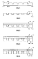
- a support 10 may be etched to form a plurality of discrete holes or trenches 12 on the top side 13 of the support 10.
- the support 10, in one embodiment of the present invention, may be formed by a P-type silicon semiconductor substrate.
- the support may include sapphire, for example in a semiconductor over insulator (SOI) technology.
- SOI semiconductor over insulator
- the trenches 12 may be oxidized to form an oxide 14, as shown in Figure 2.
- the trenches 12 that have now been oxidized may be relatively deep trenches extending a substantial distance through the support 10.
- the trenches 12 may extend, after oxidation, through more than half the thickness of the support 10 from the top side 13 to the back side 11.
- the oxide 14 may be deposited.
- a dielectric such as silicon nitride may be used in place of the oxide 14.
- the trenches 12 may be covered by a layer of metallization which forms the so-called metal one metallization as indicated at 16 in Figure 3.
- the metal one metallization 16 may be covered by an interlayer dielectric (ILD) and additional metallization layers 18.
- the additional metallization layers may include second, third and fourth or even higher layers of metallization with intervening dielectric layers.
- the metallization layers may implement the desired structure and function for a conventional microprocessor.
- trenches 20 are formed from the back side 11 of the support 10 to mate up with the array of trenches 12 previously formed in the top side 13. As a result, the holes or trenches 20 extend completely through the support 10.
- the trenches 20 may be formed by chemical or laser ablation from the back side 11. Advantageously, they do not adversely affect the metal one layer 16.
- the exposed surfaces of the trench 20 are oxidized to form a trench oxide 14 which covers the interior surface of the trench 20.
- the oxide 14 may also be a deposited oxide.
- other dielectric materials such as silicon nitride may be deposited in place of or in addition to oxide.
- the trenches may be formed in a circular cross-sectional shape, in one embodiment of the invention.
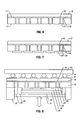
- the trenches 20 may be metallized, as indicated at 24, to form conductive vias 24 that extend from the top side 13 through to the back side 11 of the support 10.
- the conductive vias 24 electrically contact the metal one layer 16 and on the bottom the vias electrically contact the mirror pads 26.
- a variety of conventional materials may be utilized to form the vias 24 including aluminum, copper and gold.
- the vias 24 may be formed of a solid conductive plug substantially filling the trenches 20.
- the backside 11 is metallized and a plurality of metal pads 26 are patterned and defined.
- the metal pads 26 form the so-called metal zero layer or mirror pads for the spatial light modulator.
- the metal pads 26 may be formed using liquid crystal over silicon (LCOS) technology.
- An alignment layer 28 may be formed over the mirror pads 26.
- the alignment layer 28 may be formed, for example, of an indium tin oxide.
- a liquid crystal material 30 is sandwiched between an alignment layer 32 coated on a transparent top plate 34 and the layer 28.
- the layer 32 may also be formed of indium tin oxide. Spacers (not shown) may be provided between the alignment layer 28 and the top plate 34 to maintain the desired spacing.
- a heat sink 36 may be peripherally secured to the support 10 to remove heat generated by the microprocessor and/or the spatial light modulator without interfering with photon access, indicated by double arrows, to the modulator.
- An electrical contact 38 may be provided to electrical couple to the alignment layers 32 and 28.
- a seal 40 may be provided to maintain the liquid crystal material 30 between the alignment layers 28 and 32.
- the support 10 may be made of P-type silicon semiconductor material and N-plus type diffusions 50 may be formed between the metal interconnects 24.
- the diffusions 50 may form the transistors which control the operation of the spatial light modulator.
- a plurality of metal contacts 42 may be patterned and defined on top of the microprocessor for allowing input and output connections to the microprocessor.
- the contacts 42 may be formed from a metal five metallization layer.
- solder balls or bumps 44 may be utilized to implement a flip chip type package that couples the microprocessor inputs and outputs to a printed circuit board 46.
- the bumps 44 may also implement the input/output connections for the spatial light modulator through the vias 24.
- a tape automated bonding (TAB) system may be used in place of the bumps 44.
- the mirror pads 26 define the mirrors for the spatial light modulator. Potentials applied to the liquid crystal material 30 modulates the incoming light to create images. These images can be directly viewed or projected onto a projection screen. Commonly, the metal pads 26 may be rectangular or square and together form a rectangular array of mirrors. The mirror array may define an array of pixel elements in conjunction with the liquid crystal material positioned over the mirrors. The transmissivity of the liquid crystal material 30 may be controlled by the LCOS active elements formed in the support 10.
- pixels storage capacitors that normally consume the bulk of the area in silicon liquid crystal device backplane displays, are naturally formed by the metal vias 24 and the mirror pads 26 over oxide 14b on the back side 11. This may reduce the need for large electrical devices and may allow for additional pixel plane processing transistors or the integration of other functions, such as a graphics display control or processor functions.
- Some embodiments may be particularly amenable for use in micro displays and rear projection displays, by making the optical system very compact, both in frame sequential and multi-channel applications.
Landscapes
- Physics & Mathematics (AREA)
- Nonlinear Science (AREA)
- Optics & Photonics (AREA)
- Crystallography & Structural Chemistry (AREA)
- Chemical & Material Sciences (AREA)
- General Physics & Mathematics (AREA)
- Mathematical Physics (AREA)
- Engineering & Computer Science (AREA)
- Microelectronics & Electronic Packaging (AREA)
- Power Engineering (AREA)
- Liquid Crystal (AREA)
- Optical Integrated Circuits (AREA)
- Solid State Image Pick-Up Elements (AREA)
- Facsimile Scanning Arrangements (AREA)
Abstract
Description
Claims (6)
- An integrated circuit comprising:a support (10) formed of a semiconductor material having opposed sides (13, 11);a spatial light modulator formed on one side (11) of said support (10);a processor formed on the opposite side (13) of said support (10); anda conductor (24) electrically coupling said modulator and said processor through said support (10).
- The circuit of claim 1 wherein said spatial light modulator is formed using liquid crystal on silicon technology.
- The circuit of claim 1 wherein said integrated circuit includes a plurality of conductors (24) formed as dielectric insulated vias which extend from one opposed side to the other opposed side of said support (10).
- The circuit of claim 1 including a plurality of conductive vias which extend through said support (10), a plurality of mirror pads (26) in said modulator and a plurality of conductive pads (18) in said processor, each of said vias contacting a mirror pad in said spatial light modulator on one side of said support (10), and a metal pad on the other side of said support (10).
- The circuit of claim 1 including a plurality of solder bumps (44) on said processor for making electrical contact to external devices.
- The circuit of claim 1 including a hole formed completely through said support (10) forming a tubular wall, a dielectric layer (14) formed on said wall and a conductive layer (26) formed within said hole such that said dielectric layer is sandwiched between said conductive layer and said support (10), a mirror pad being formed in electrical contact with said conductive layer, said mirror pad forming part of said spatial light modulator.
Applications Claiming Priority (3)
| Application Number | Priority Date | Filing Date | Title |
|---|---|---|---|
| US430284 | 1999-10-29 | ||
| US09/430,284 US6348991B1 (en) | 1999-10-29 | 1999-10-29 | Integrated circuit with opposed spatial light modulator and processor |
| EP00970564A EP1224504B1 (en) | 1999-10-29 | 2000-10-04 | Method of manufacturing integrated circuit with opposed spatial light modulator and processor |
Related Parent Applications (1)
| Application Number | Title | Priority Date | Filing Date |
|---|---|---|---|
| EP00970564.1 Division | 2000-10-04 |
Publications (1)
| Publication Number | Publication Date |
|---|---|
| EP1515183A1 true EP1515183A1 (en) | 2005-03-16 |
Family
ID=23706873
Family Applications (2)
| Application Number | Title | Priority Date | Filing Date |
|---|---|---|---|
| EP00970564A Expired - Lifetime EP1224504B1 (en) | 1999-10-29 | 2000-10-04 | Method of manufacturing integrated circuit with opposed spatial light modulator and processor |
| EP04029880A Withdrawn EP1515183A1 (en) | 1999-10-29 | 2000-10-04 | Integrated circuit |
Family Applications Before (1)
| Application Number | Title | Priority Date | Filing Date |
|---|---|---|---|
| EP00970564A Expired - Lifetime EP1224504B1 (en) | 1999-10-29 | 2000-10-04 | Method of manufacturing integrated circuit with opposed spatial light modulator and processor |
Country Status (10)
| Country | Link |
|---|---|
| US (2) | US6348991B1 (en) |
| EP (2) | EP1224504B1 (en) |
| JP (1) | JP3611819B2 (en) |
| KR (1) | KR100492378B1 (en) |
| AT (1) | ATE286266T1 (en) |
| AU (1) | AU7992500A (en) |
| DE (1) | DE60017172T2 (en) |
| HK (1) | HK1046038B (en) |
| TW (1) | TW478020B (en) |
| WO (1) | WO2001033293A1 (en) |
Families Citing this family (23)
| Publication number | Priority date | Publication date | Assignee | Title |
|---|---|---|---|---|
| US6639714B2 (en) * | 1999-10-29 | 2003-10-28 | Intel Corporation | Integrated circuit with opposed spatial light modulator and processor |
| US6795605B1 (en) * | 2000-08-01 | 2004-09-21 | Cheetah Omni, Llc | Micromechanical optical switch |
| US7145704B1 (en) * | 2003-11-25 | 2006-12-05 | Cheetah Omni, Llc | Optical logic gate based optical router |
| US7003188B2 (en) * | 2001-04-17 | 2006-02-21 | Ying Wen Hsu | Low loss optical switching system |
| US6819824B1 (en) * | 2001-05-21 | 2004-11-16 | Calient Networks | Optical switch package |
| US6814445B2 (en) * | 2001-06-30 | 2004-11-09 | Texas Instruments Incorporated | DMD heat sink socket assembly |
| US6721077B2 (en) * | 2001-09-11 | 2004-04-13 | Intel Corporation | Light emitting device addressed spatial light modulator |
| US20030122206A1 (en) * | 2001-11-09 | 2003-07-03 | Amal Bhattarai | Multi-chip module integrating MEMS mirror array with electronics |
| US7110671B1 (en) * | 2001-12-03 | 2006-09-19 | Cheetah Omni, Llc | Method and apparatus for scheduling communication using a star switching fabric |
| US20030107794A1 (en) * | 2001-12-11 | 2003-06-12 | Siekkinen James W. | Micro mirror array |
| US7065113B2 (en) * | 2002-04-30 | 2006-06-20 | Mohammed Ershad Ali | Method and apparatus for interconnecting a laser array and an integrated circuit of a laser-based transmitter |
| US7064212B2 (en) * | 2002-06-20 | 2006-06-20 | The Regents Of The University Of California | Electrochromic salts, solutions, and devices |
| US20040125283A1 (en) * | 2002-12-30 | 2004-07-01 | Samson Huang | LCOS imaging device |
| US20040125093A1 (en) * | 2002-12-30 | 2004-07-01 | Serge Rutman | Micro-controller with integrated light modulator |
| US6897148B2 (en) * | 2003-04-09 | 2005-05-24 | Tru-Si Technologies, Inc. | Electroplating and electroless plating of conductive materials into openings, and structures obtained thereby |
| US7071908B2 (en) | 2003-05-20 | 2006-07-04 | Kagutech, Ltd. | Digital backplane |
| US7154587B2 (en) * | 2003-06-30 | 2006-12-26 | Asml Netherlands B.V | Spatial light modulator, lithographic apparatus and device manufacturing method |
| US20050046016A1 (en) * | 2003-09-03 | 2005-03-03 | Ken Gilleo | Electronic package with insert conductor array |
| US20050162727A1 (en) * | 2004-01-24 | 2005-07-28 | Fusao Ishii | Micromirrors with support walls |
| JP4902953B2 (en) * | 2004-09-30 | 2012-03-21 | ラピスセミコンダクタ株式会社 | Manufacturing method of semiconductor device |
| TWI385435B (en) * | 2008-05-08 | 2013-02-11 | Universal Scient Ind Shanghai | Lcos device and assembly of lcos device and circuit board |
| US10025033B2 (en) | 2016-03-01 | 2018-07-17 | Advanced Semiconductor Engineering, Inc. | Optical fiber structure, optical communication apparatus and manufacturing process for manufacturing the same |
| US10241264B2 (en) | 2016-07-01 | 2019-03-26 | Advanced Semiconductor Engineering, Inc. | Semiconductor device packages |
Citations (4)
| Publication number | Priority date | Publication date | Assignee | Title |
|---|---|---|---|---|
| DE2715446A1 (en) | 1977-04-06 | 1978-10-12 | Siemens Ag | Liquid crystal display device - with control modules integrated in semiconductor cell wall requiring fewer connections |
| WO1994017440A1 (en) | 1993-01-19 | 1994-08-04 | Hughes Aircraft Company | Reflective liquid crystal display including driver devices integrally formed in monocrystalline semiconductor layer and method of fabricating the display |
| WO1996004585A1 (en) * | 1994-08-02 | 1996-02-15 | Shichao Ge | Outside-active-matrix-lcd |
| US5737052A (en) * | 1994-12-07 | 1998-04-07 | International Business Machines Corporation | Liquid crystal display and manufacturing process thereof with drive circuit and active matrix connected via through hole |
Family Cites Families (3)
| Publication number | Priority date | Publication date | Assignee | Title |
|---|---|---|---|---|
| US6348907B1 (en) * | 1989-08-22 | 2002-02-19 | Lawson A. Wood | Display apparatus with digital micromirror device |
| US6153927A (en) * | 1999-09-30 | 2000-11-28 | Intel Corporation | Packaged integrated processor and spatial light modulator |
| US6738104B2 (en) * | 2000-02-25 | 2004-05-18 | Texas Instruments Incorporated | Robust color wheel phase error method for improved channel change re-lock performance |
-
1999
- 1999-10-29 US US09/430,284 patent/US6348991B1/en not_active Expired - Lifetime
-
2000
- 2000-10-04 HK HK02107571.0A patent/HK1046038B/en not_active IP Right Cessation
- 2000-10-04 KR KR10-2002-7005489A patent/KR100492378B1/en not_active Expired - Fee Related
- 2000-10-04 EP EP00970564A patent/EP1224504B1/en not_active Expired - Lifetime
- 2000-10-04 AU AU79925/00A patent/AU7992500A/en not_active Abandoned
- 2000-10-04 AT AT00970564T patent/ATE286266T1/en not_active IP Right Cessation
- 2000-10-04 DE DE60017172T patent/DE60017172T2/en not_active Expired - Lifetime
- 2000-10-04 EP EP04029880A patent/EP1515183A1/en not_active Withdrawn
- 2000-10-04 WO PCT/US2000/027336 patent/WO2001033293A1/en not_active Ceased
- 2000-10-04 JP JP2001535119A patent/JP3611819B2/en not_active Expired - Fee Related
- 2000-10-19 TW TW089121926A patent/TW478020B/en not_active IP Right Cessation
-
2001
- 2001-09-25 US US09/961,499 patent/US6388798B2/en not_active Expired - Lifetime
Patent Citations (4)
| Publication number | Priority date | Publication date | Assignee | Title |
|---|---|---|---|---|
| DE2715446A1 (en) | 1977-04-06 | 1978-10-12 | Siemens Ag | Liquid crystal display device - with control modules integrated in semiconductor cell wall requiring fewer connections |
| WO1994017440A1 (en) | 1993-01-19 | 1994-08-04 | Hughes Aircraft Company | Reflective liquid crystal display including driver devices integrally formed in monocrystalline semiconductor layer and method of fabricating the display |
| WO1996004585A1 (en) * | 1994-08-02 | 1996-02-15 | Shichao Ge | Outside-active-matrix-lcd |
| US5737052A (en) * | 1994-12-07 | 1998-04-07 | International Business Machines Corporation | Liquid crystal display and manufacturing process thereof with drive circuit and active matrix connected via through hole |
Also Published As
| Publication number | Publication date |
|---|---|
| AU7992500A (en) | 2001-05-14 |
| HK1046038A1 (en) | 2002-12-20 |
| TW478020B (en) | 2002-03-01 |
| DE60017172T2 (en) | 2005-05-25 |
| US6348991B1 (en) | 2002-02-19 |
| KR20020065496A (en) | 2002-08-13 |
| HK1046038B (en) | 2005-05-13 |
| ATE286266T1 (en) | 2005-01-15 |
| JP2003513337A (en) | 2003-04-08 |
| DE60017172D1 (en) | 2005-02-03 |
| US6388798B2 (en) | 2002-05-14 |
| EP1224504A1 (en) | 2002-07-24 |
| JP3611819B2 (en) | 2005-01-19 |
| WO2001033293A1 (en) | 2001-05-10 |
| EP1224504B1 (en) | 2004-12-29 |
| KR100492378B1 (en) | 2005-05-30 |
| US20020012158A1 (en) | 2002-01-31 |
Similar Documents
| Publication | Publication Date | Title |
|---|---|---|
| US6348991B1 (en) | Integrated circuit with opposed spatial light modulator and processor | |
| US20230138732A1 (en) | Transistor level interconnection methodologies utilizing 3d interconnects | |
| JP2005150717A (en) | IC device and manufacturing method thereof | |
| JP6140965B2 (en) | Semiconductor device and manufacturing method thereof | |
| KR20170017122A (en) | Semiconductor device | |
| US6639714B2 (en) | Integrated circuit with opposed spatial light modulator and processor | |
| WO2021092779A1 (en) | Chip package on package structure and electronic device | |
| CN113826207A (en) | Display panel, manufacturing method thereof and display device | |
| CN111987085A (en) | Sensor, preparation method of sensor and electronic equipment | |
| CN114664808B (en) | Semiconductor structure and manufacturing method thereof, chip packaging structure, and electronic device | |
| CN118678778A (en) | Array substrate, preparation method thereof, display panel and display device | |
| CN119673912A (en) | Adapter plate and preparation method thereof, chip packaging structure, and electronic equipment | |
| CN117855137B (en) | Chips and their fabrication methods, electronic devices | |
| JP6385515B2 (en) | Semiconductor device and manufacturing method thereof | |
| CN118489153A (en) | Chip stacking and packaging structure, preparation method thereof and electronic equipment | |
| US11415844B2 (en) | Liquid crystal display | |
| CN115377127A (en) | Array substrate, preparation method thereof and display panel | |
| US20250210531A1 (en) | Display device | |
| CN100382253C (en) | Welding pad structure and manufacturing method thereof | |
| US20090141009A1 (en) | LCD Driver IC and Method for Manufacturing the Same | |
| CN120729216A (en) | Wafer-level packaging structure, manufacturing method thereof, radio frequency component and electronic equipment | |
| JP3909593B2 (en) | Manufacturing method of semiconductor device | |
| CN121666886A (en) | Array substrate, manufacturing method thereof and display panel | |
| CN121099862A (en) | Display panel, preparation method of display panel and electronic equipment | |
| KR20020016336A (en) | Pad of Semiconductor Device and Method for the Same |
Legal Events
| Date | Code | Title | Description |
|---|---|---|---|
| PUAI | Public reference made under article 153(3) epc to a published international application that has entered the european phase |
Free format text: ORIGINAL CODE: 0009012 |
|
| AC | Divisional application: reference to earlier application |
Ref document number: 1224504 Country of ref document: EP Kind code of ref document: P |
|
| AK | Designated contracting states |
Kind code of ref document: A1 Designated state(s): AT BE CH CY DE DK ES FI FR GB GR IE IT LI LU MC NL PT SE |
|
| 17P | Request for examination filed |
Effective date: 20050308 |
|
| AKX | Designation fees paid |
Designated state(s): AT BE CH CY DE DK ES FI FR GB GR IE IT LI LU MC NL PT SE |
|
| 17Q | First examination report despatched |
Effective date: 20130212 |
|
| STAA | Information on the status of an ep patent application or granted ep patent |
Free format text: STATUS: THE APPLICATION IS DEEMED TO BE WITHDRAWN |
|
| 18D | Application deemed to be withdrawn |
Effective date: 20170503 |