EP1513252A1 - Logarithmischer linearer CMOS-Verstärker mit variabler Verstärkung - Google Patents
Logarithmischer linearer CMOS-Verstärker mit variabler Verstärkung Download PDFInfo
- Publication number
- EP1513252A1 EP1513252A1 EP03425568A EP03425568A EP1513252A1 EP 1513252 A1 EP1513252 A1 EP 1513252A1 EP 03425568 A EP03425568 A EP 03425568A EP 03425568 A EP03425568 A EP 03425568A EP 1513252 A1 EP1513252 A1 EP 1513252A1
- Authority
- EP
- European Patent Office
- Prior art keywords
- transistors
- diode
- current
- connected load
- pair
- Prior art date
- Legal status (The legal status is an assumption and is not a legal conclusion. Google has not performed a legal analysis and makes no representation as to the accuracy of the status listed.)
- Granted
Links
- 230000014509 gene expression Effects 0.000 description 6
- 238000010586 diagram Methods 0.000 description 2
- 230000001627 detrimental effect Effects 0.000 description 1
- 230000002708 enhancing effect Effects 0.000 description 1
- 230000003993 interaction Effects 0.000 description 1
Images

Classifications
-
- H—ELECTRICITY
- H03—ELECTRONIC CIRCUITRY
- H03G—CONTROL OF AMPLIFICATION
- H03G7/00—Volume compression or expansion in amplifiers
- H03G7/06—Volume compression or expansion in amplifiers having semiconductor devices
-
- H—ELECTRICITY
- H03—ELECTRONIC CIRCUITRY
- H03G—CONTROL OF AMPLIFICATION
- H03G7/00—Volume compression or expansion in amplifiers
- H03G7/001—Volume compression or expansion in amplifiers without controlling loop
Definitions
- the present invention relates in general to integrated analog circuits and more in particular to an integrated logarithmic linear variable gain CMOS amplifier.
- the linear logarithmic gain (dB gain) variation range of the function is relatively restricted.
- the value of x of the gain expression for remaining in substantially linear dB gain variation range is limited to -0.7 ⁇ x ⁇ 0.7.
- the variation of the bias current in a transistor notably alters its transconductance thus obtaining the desired behaviour of the circuit according to equation 1, but the variation of the bias current affects also the bandwith and the linearity of the amplifier.
- the group delay of the amplifier circuit is (inversely) proportional to the bandwith.
- Variable gain amplifiers work with fixed output voltage swing (fixed by the control loop) and the gain is inversely proportional to the input voltage swing.
- the diode loads, common to the two cross connected differential input stages have transistor means connencted in parallel to the diode loads for subtrackting a constant current of a desired value from the current that would otherwise be flowing through the diode loads. This permits to translate the gain curve of the amplifier according to needs.
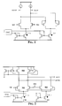
- Figure 1 represents, as already noted above, the basic circuit of a state of the art integrated logarithmic linear variable gain CMOS amplifier.
- Figure 2 shows the circuit diagram of a logarithmic linear variable gain CMOS amplifier according to a preferred embodiment of this invention.
- Figure 3 is a diagram of the gain characteristics of an amplifier according to the present invetion.
- the two differential transistor pairs, M1 and M2, sharing the same diode-connected load transistors M3, are cross connected to the inpuit nodes INP and INM of the amplifier, according to an essential feature of the novel circuit of this invention.
- the two differential pairs of transistors M1 and M2 are biased by respective currents output by a linear digital-to-analog converter through respective current mirrors M4 and M5, and the pair M3 of diode connected load transistors is biased by the difference between the sum of these currents and the currents flowing in M6 and M7.
- the sum current I TOT will be equal to the actual bias current I 3 plus the constant amount that is subtracted by flowing through the optionally added transistors M6 and M7.
- the effective bias current I 3 of the bandwidth equation 3 will be constant, ensuring constancy of the bandwidth.
- additional transistors M6 and M7 respectfully connected in parallel to the diode-connected load transistors M3, are used to subtrac a certain constant amount for the total current that would be flowing through the diode-connected load transistors M3.
- the current that actually flows through the diode-connected load transistors M3 may be fixed for setting the gm of the M3 transistors and therefore to translate the gain characteristic.
- the expression 5 may be plotted as shown in Figure 3 in order to show the linear variation range of the dB gain figure.
- the amplifier provides for an output signal of fixed amplitude while the input signal varies its amplitude.
- the gain is reduced by reducing the current in the first differential input pair M1 and complementarily increasing the current in the second input differential pair M2.
- the novel amplifier of this invention has a markedly improved linearity in comparison with the known amplifier circuit of Figure 1.
- variable gain logarithmic linear amplifier with improved linearity characteristic of this invention may have innumerable applications, a particularly important application in which the amplifier of this invention is particularly useful is in data acquisition channels from a mass storage drive, such as a hard disk.
Landscapes
- Amplifiers (AREA)
- Control Of Amplification And Gain Control (AREA)
Priority Applications (3)
| Application Number | Priority Date | Filing Date | Title |
|---|---|---|---|
| EP03425568A EP1513252B1 (de) | 2003-09-02 | 2003-09-02 | Logarithmischer linearer CMOS-Verstärker mit variabler Verstärkung |
| DE60335185T DE60335185D1 (de) | 2003-09-02 | 2003-09-02 | Logarithmischer linearer CMOS-Verstärker mit variabler Verstärkung |
| US10/931,469 US7737759B2 (en) | 2003-09-02 | 2004-09-01 | Logarithmic linear variable gain CMOS amplifier |
Applications Claiming Priority (1)
| Application Number | Priority Date | Filing Date | Title |
|---|---|---|---|
| EP03425568A EP1513252B1 (de) | 2003-09-02 | 2003-09-02 | Logarithmischer linearer CMOS-Verstärker mit variabler Verstärkung |
Publications (2)
| Publication Number | Publication Date |
|---|---|
| EP1513252A1 true EP1513252A1 (de) | 2005-03-09 |
| EP1513252B1 EP1513252B1 (de) | 2010-12-01 |
Family
ID=34130422
Family Applications (1)
| Application Number | Title | Priority Date | Filing Date |
|---|---|---|---|
| EP03425568A Expired - Lifetime EP1513252B1 (de) | 2003-09-02 | 2003-09-02 | Logarithmischer linearer CMOS-Verstärker mit variabler Verstärkung |
Country Status (3)
| Country | Link |
|---|---|
| US (1) | US7737759B2 (de) |
| EP (1) | EP1513252B1 (de) |
| DE (1) | DE60335185D1 (de) |
Cited By (1)
| Publication number | Priority date | Publication date | Assignee | Title |
|---|---|---|---|---|
| WO2007004189A3 (en) * | 2005-07-04 | 2007-05-03 | Koninkl Philips Electronics Nv | Device comprising a feedback-less gain controlled amplifier |
Families Citing this family (7)
| Publication number | Priority date | Publication date | Assignee | Title |
|---|---|---|---|---|
| KR100732068B1 (ko) * | 2006-06-30 | 2007-06-27 | (주)에프씨아이 | 지수적인 선형성을 갖는 가변 이득 증폭기 |
| US8213638B2 (en) * | 2007-02-20 | 2012-07-03 | Texas Instruments Incorporated | Equalizer |
| US8779833B2 (en) | 2012-03-12 | 2014-07-15 | King Fahd University of Petroleum and Minearals | Current-mode CMOS logarithmic function circuit |
| US9298952B2 (en) * | 2013-11-18 | 2016-03-29 | King Fahd University Of Petroleum And Minerals | CMOS logarithmic current generator and method for generating a logarithmic current |
| US10063253B1 (en) * | 2017-06-22 | 2018-08-28 | Intel Corporation | Summer circuit including linearized load |
| US12598099B2 (en) | 2023-09-15 | 2026-04-07 | Nxp Usa, Inc. | Programmable equalizer |
| US12574270B2 (en) * | 2023-09-15 | 2026-03-10 | Nxp Usa, Inc. | Programmable equalizer |
Citations (4)
| Publication number | Priority date | Publication date | Assignee | Title |
|---|---|---|---|---|
| US5886579A (en) * | 1996-05-28 | 1999-03-23 | Analog Devices, Inc. | Variable gain CMOS amplifier |
| EP1024450A1 (de) * | 1999-01-30 | 2000-08-02 | Lucent Technologies Inc. | Analoge Dekodierungsvorrichtung |
| US20020048109A1 (en) * | 2000-10-19 | 2002-04-25 | Chaiken Alan I. | dB linear variable gain amplifier |
| US6584486B1 (en) * | 1999-08-06 | 2003-06-24 | Anadec Gmbh | Method for mathematically processing two quantities in an electronic circuit |
Family Cites Families (3)
| Publication number | Priority date | Publication date | Assignee | Title |
|---|---|---|---|---|
| ES2136066T3 (es) * | 1991-05-23 | 1999-11-16 | Nec Corp | Amplificador logaritmico de frecuencia intermedia. |
| US6894552B2 (en) * | 2003-02-28 | 2005-05-17 | Teradyne, Inc. | Low-jitter delay cell |
| US6985036B2 (en) * | 2003-11-26 | 2006-01-10 | Scintera Networks, Inc. | Digitally controlled transconductance cell |
-
2003
- 2003-09-02 EP EP03425568A patent/EP1513252B1/de not_active Expired - Lifetime
- 2003-09-02 DE DE60335185T patent/DE60335185D1/de not_active Expired - Lifetime
-
2004
- 2004-09-01 US US10/931,469 patent/US7737759B2/en not_active Expired - Lifetime
Patent Citations (4)
| Publication number | Priority date | Publication date | Assignee | Title |
|---|---|---|---|---|
| US5886579A (en) * | 1996-05-28 | 1999-03-23 | Analog Devices, Inc. | Variable gain CMOS amplifier |
| EP1024450A1 (de) * | 1999-01-30 | 2000-08-02 | Lucent Technologies Inc. | Analoge Dekodierungsvorrichtung |
| US6584486B1 (en) * | 1999-08-06 | 2003-06-24 | Anadec Gmbh | Method for mathematically processing two quantities in an electronic circuit |
| US20020048109A1 (en) * | 2000-10-19 | 2002-04-25 | Chaiken Alan I. | dB linear variable gain amplifier |
Cited By (2)
| Publication number | Priority date | Publication date | Assignee | Title |
|---|---|---|---|---|
| WO2007004189A3 (en) * | 2005-07-04 | 2007-05-03 | Koninkl Philips Electronics Nv | Device comprising a feedback-less gain controlled amplifier |
| US7821342B2 (en) | 2005-07-04 | 2010-10-26 | St-Ericsson Sa | Device comprising a feedback-less gain controlled amplifier |
Also Published As
| Publication number | Publication date |
|---|---|
| US7737759B2 (en) | 2010-06-15 |
| DE60335185D1 (de) | 2011-01-13 |
| EP1513252B1 (de) | 2010-12-01 |
| US20050052216A1 (en) | 2005-03-10 |
Similar Documents
| Publication | Publication Date | Title |
|---|---|---|
| US4904952A (en) | Differential amplifier incorporating negative resistance | |
| US5418494A (en) | Variable gain amplifier for low supply voltage systems | |
| US6753730B2 (en) | Differential amplifier and filter circuit using the same | |
| US5933056A (en) | Single pole current mode common-mode feedback circuit | |
| JP2656714B2 (ja) | 全差動増幅器 | |
| KR100427878B1 (ko) | 증폭회로 | |
| US5942929A (en) | Active phase splitter | |
| JPH0786850A (ja) | 完全差動演算増幅器、および差動演算増幅器における同相再構築の方法 | |
| KR100693821B1 (ko) | 차동 증폭기 및 이를 위한 액티브 로드 | |
| US6819168B1 (en) | Integrator with high gain and fast transient response | |
| US6121818A (en) | Mixer using replica voltage-current converter | |
| EP1513252A1 (de) | Logarithmischer linearer CMOS-Verstärker mit variabler Verstärkung | |
| JP3410704B2 (ja) | 高速カレントミラー回路及び方法 | |
| US7135927B2 (en) | Ultra fast, low noise operational amplifier with dynamic biasing | |
| US6362682B2 (en) | Common-mode feedback circuit and method | |
| US7292098B2 (en) | Operational amplifier | |
| JP2007528682A (ja) | ハイリニア可変利得増幅器 | |
| US7038542B2 (en) | Variable gain amplifier | |
| US7880545B1 (en) | Cascode compensation circuit and method for amplifier stability | |
| Centurelli et al. | A bootstrap technique for wideband amplifiers | |
| KR20010076268A (ko) | 제어가능한 기준전압을 갖는 고주파가변감쇠기 | |
| US7202746B1 (en) | Multiple-stage operational amplifier and methods and systems utilizing the same | |
| US7492226B2 (en) | Linearization apparatus of triode region type operational transconductance amplifier | |
| US5917376A (en) | Circuit and technique for compensating high gain amplifier without compensation capacitors | |
| US6078220A (en) | Complementary class AB current amplifier |
Legal Events
| Date | Code | Title | Description |
|---|---|---|---|
| PUAI | Public reference made under article 153(3) epc to a published international application that has entered the european phase |
Free format text: ORIGINAL CODE: 0009012 |
|
| AK | Designated contracting states |
Kind code of ref document: A1 Designated state(s): AT BE BG CH CY CZ DE DK EE ES FI FR GB GR HU IE IT LI LU MC NL PT RO SE SI SK TR |
|
| AX | Request for extension of the european patent |
Extension state: AL LT LV MK |
|
| 17P | Request for examination filed |
Effective date: 20050809 |
|
| AKX | Designation fees paid |
Designated state(s): DE FR GB IT |
|
| 17Q | First examination report despatched |
Effective date: 20060912 |
|
| RAP1 | Party data changed (applicant data changed or rights of an application transferred) |
Owner name: STMICROELECTRONICS SRL |
|
| GRAP | Despatch of communication of intention to grant a patent |
Free format text: ORIGINAL CODE: EPIDOSNIGR1 |
|
| GRAS | Grant fee paid |
Free format text: ORIGINAL CODE: EPIDOSNIGR3 |
|
| GRAA | (expected) grant |
Free format text: ORIGINAL CODE: 0009210 |
|
| AK | Designated contracting states |
Kind code of ref document: B1 Designated state(s): DE FR GB IT |
|
| REG | Reference to a national code |
Ref country code: GB Ref legal event code: FG4D |
|
| REF | Corresponds to: |
Ref document number: 60335185 Country of ref document: DE Date of ref document: 20110113 Kind code of ref document: P |
|
| PLBE | No opposition filed within time limit |
Free format text: ORIGINAL CODE: 0009261 |
|
| STAA | Information on the status of an ep patent application or granted ep patent |
Free format text: STATUS: NO OPPOSITION FILED WITHIN TIME LIMIT |
|
| 26N | No opposition filed |
Effective date: 20110902 |
|
| PGFP | Annual fee paid to national office [announced via postgrant information from national office to epo] |
Ref country code: GB Payment date: 20110830 Year of fee payment: 9 |
|
| REG | Reference to a national code |
Ref country code: DE Ref legal event code: R097 Ref document number: 60335185 Country of ref document: DE Effective date: 20110902 |
|
| PG25 | Lapsed in a contracting state [announced via postgrant information from national office to epo] |
Ref country code: IT Free format text: LAPSE BECAUSE OF FAILURE TO SUBMIT A TRANSLATION OF THE DESCRIPTION OR TO PAY THE FEE WITHIN THE PRESCRIBED TIME-LIMIT Effective date: 20101201 |
|
| REG | Reference to a national code |
Ref country code: FR Ref legal event code: ST Effective date: 20120531 |
|
| PG25 | Lapsed in a contracting state [announced via postgrant information from national office to epo] |
Ref country code: FR Free format text: LAPSE BECAUSE OF NON-PAYMENT OF DUE FEES Effective date: 20110930 |
|
| PGFP | Annual fee paid to national office [announced via postgrant information from national office to epo] |
Ref country code: DE Payment date: 20120827 Year of fee payment: 10 |
|
| GBPC | Gb: european patent ceased through non-payment of renewal fee |
Effective date: 20120902 |
|
| PG25 | Lapsed in a contracting state [announced via postgrant information from national office to epo] |
Ref country code: GB Free format text: LAPSE BECAUSE OF NON-PAYMENT OF DUE FEES Effective date: 20120902 |
|
| REG | Reference to a national code |
Ref country code: DE Ref legal event code: R119 Ref document number: 60335185 Country of ref document: DE Effective date: 20140401 |
|
| PG25 | Lapsed in a contracting state [announced via postgrant information from national office to epo] |
Ref country code: DE Free format text: LAPSE BECAUSE OF NON-PAYMENT OF DUE FEES Effective date: 20140401 |