EP1513233A1 - Durch LEPECVD und MOCVD auf Silizium hergestellte GaAs/GaAs-Laser - Google Patents
Durch LEPECVD und MOCVD auf Silizium hergestellte GaAs/GaAs-Laser Download PDFInfo
- Publication number
- EP1513233A1 EP1513233A1 EP03020169A EP03020169A EP1513233A1 EP 1513233 A1 EP1513233 A1 EP 1513233A1 EP 03020169 A EP03020169 A EP 03020169A EP 03020169 A EP03020169 A EP 03020169A EP 1513233 A1 EP1513233 A1 EP 1513233A1
- Authority
- EP
- European Patent Office
- Prior art keywords
- layer
- gallium arsenide
- substrate
- formation
- vapour deposition
- Prior art date
- Legal status (The legal status is an assumption and is not a legal conclusion. Google has not performed a legal analysis and makes no representation as to the accuracy of the status listed.)
- Granted
Links
Images

Classifications
-
- B—PERFORMING OPERATIONS; TRANSPORTING
- B82—NANOTECHNOLOGY
- B82Y—SPECIFIC USES OR APPLICATIONS OF NANOSTRUCTURES; MEASUREMENT OR ANALYSIS OF NANOSTRUCTURES; MANUFACTURE OR TREATMENT OF NANOSTRUCTURES
- B82Y20/00—Nanooptics, e.g. quantum optics or photonic crystals
-
- H—ELECTRICITY
- H10—SEMICONDUCTOR DEVICES; ELECTRIC SOLID-STATE DEVICES NOT OTHERWISE PROVIDED FOR
- H10P—GENERIC PROCESSES OR APPARATUS FOR THE MANUFACTURE OR TREATMENT OF DEVICES COVERED BY CLASS H10
- H10P14/00—Formation of materials, e.g. in the shape of layers or pillars
- H10P14/20—Formation of materials, e.g. in the shape of layers or pillars of semiconductor materials
- H10P14/29—Formation of materials, e.g. in the shape of layers or pillars of semiconductor materials characterised by the substrates
- H10P14/2901—Materials
- H10P14/2902—Materials being Group IVA materials
- H10P14/2905—Silicon, silicon germanium or germanium
-
- H—ELECTRICITY
- H01—ELECTRIC ELEMENTS
- H01S—DEVICES USING THE PROCESS OF LIGHT AMPLIFICATION BY STIMULATED EMISSION OF RADIATION [LASER] TO AMPLIFY OR GENERATE LIGHT; DEVICES USING STIMULATED EMISSION OF ELECTROMAGNETIC RADIATION IN WAVE RANGES OTHER THAN OPTICAL
- H01S5/00—Semiconductor lasers
- H01S5/30—Structure or shape of the active region; Materials used for the active region
- H01S5/34—Structure or shape of the active region; Materials used for the active region comprising quantum well or superlattice structures, e.g. single quantum well [SQW] lasers, multiple quantum well [MQW] lasers or graded index separate confinement heterostructure [GRINSCH] lasers
- H01S5/343—Structure or shape of the active region; Materials used for the active region comprising quantum well or superlattice structures, e.g. single quantum well [SQW] lasers, multiple quantum well [MQW] lasers or graded index separate confinement heterostructure [GRINSCH] lasers in AIIIBV compounds, e.g. AlGaAs-laser, InP-based laser
- H01S5/34313—Structure or shape of the active region; Materials used for the active region comprising quantum well or superlattice structures, e.g. single quantum well [SQW] lasers, multiple quantum well [MQW] lasers or graded index separate confinement heterostructure [GRINSCH] lasers in AIIIBV compounds, e.g. AlGaAs-laser, InP-based laser with a well layer having only As as V-compound, e.g. AlGaAs, InGaAs
-
- H—ELECTRICITY
- H10—SEMICONDUCTOR DEVICES; ELECTRIC SOLID-STATE DEVICES NOT OTHERWISE PROVIDED FOR
- H10P—GENERIC PROCESSES OR APPARATUS FOR THE MANUFACTURE OR TREATMENT OF DEVICES COVERED BY CLASS H10
- H10P14/00—Formation of materials, e.g. in the shape of layers or pillars
- H10P14/20—Formation of materials, e.g. in the shape of layers or pillars of semiconductor materials
- H10P14/24—Formation of materials, e.g. in the shape of layers or pillars of semiconductor materials using chemical vapour deposition [CVD]
-
- H—ELECTRICITY
- H10—SEMICONDUCTOR DEVICES; ELECTRIC SOLID-STATE DEVICES NOT OTHERWISE PROVIDED FOR
- H10P—GENERIC PROCESSES OR APPARATUS FOR THE MANUFACTURE OR TREATMENT OF DEVICES COVERED BY CLASS H10
- H10P14/00—Formation of materials, e.g. in the shape of layers or pillars
- H10P14/20—Formation of materials, e.g. in the shape of layers or pillars of semiconductor materials
- H10P14/32—Formation of materials, e.g. in the shape of layers or pillars of semiconductor materials characterised by intermediate layers between substrates and deposited layers
- H10P14/3202—Materials thereof
- H10P14/3204—Materials thereof being Group IVA semiconducting materials
- H10P14/3211—Silicon, silicon germanium or germanium
-
- H—ELECTRICITY
- H10—SEMICONDUCTOR DEVICES; ELECTRIC SOLID-STATE DEVICES NOT OTHERWISE PROVIDED FOR
- H10P—GENERIC PROCESSES OR APPARATUS FOR THE MANUFACTURE OR TREATMENT OF DEVICES COVERED BY CLASS H10
- H10P14/00—Formation of materials, e.g. in the shape of layers or pillars
- H10P14/20—Formation of materials, e.g. in the shape of layers or pillars of semiconductor materials
- H10P14/32—Formation of materials, e.g. in the shape of layers or pillars of semiconductor materials characterised by intermediate layers between substrates and deposited layers
- H10P14/3202—Materials thereof
- H10P14/3214—Materials thereof being Group IIIA-VA semiconductors
- H10P14/3221—Arsenides
-
- H—ELECTRICITY
- H10—SEMICONDUCTOR DEVICES; ELECTRIC SOLID-STATE DEVICES NOT OTHERWISE PROVIDED FOR
- H10P—GENERIC PROCESSES OR APPARATUS FOR THE MANUFACTURE OR TREATMENT OF DEVICES COVERED BY CLASS H10
- H10P14/00—Formation of materials, e.g. in the shape of layers or pillars
- H10P14/20—Formation of materials, e.g. in the shape of layers or pillars of semiconductor materials
- H10P14/32—Formation of materials, e.g. in the shape of layers or pillars of semiconductor materials characterised by intermediate layers between substrates and deposited layers
- H10P14/3242—Structure
- H10P14/3244—Layer structure
- H10P14/3251—Layer structure consisting of three or more layers
- H10P14/3252—Alternating layers, e.g. superlattice
-
- H—ELECTRICITY
- H10—SEMICONDUCTOR DEVICES; ELECTRIC SOLID-STATE DEVICES NOT OTHERWISE PROVIDED FOR
- H10P—GENERIC PROCESSES OR APPARATUS FOR THE MANUFACTURE OR TREATMENT OF DEVICES COVERED BY CLASS H10
- H10P14/00—Formation of materials, e.g. in the shape of layers or pillars
- H10P14/20—Formation of materials, e.g. in the shape of layers or pillars of semiconductor materials
- H10P14/32—Formation of materials, e.g. in the shape of layers or pillars of semiconductor materials characterised by intermediate layers between substrates and deposited layers
- H10P14/3242—Structure
- H10P14/3244—Layer structure
- H10P14/3254—Graded layers
-
- H—ELECTRICITY
- H10—SEMICONDUCTOR DEVICES; ELECTRIC SOLID-STATE DEVICES NOT OTHERWISE PROVIDED FOR
- H10P—GENERIC PROCESSES OR APPARATUS FOR THE MANUFACTURE OR TREATMENT OF DEVICES COVERED BY CLASS H10
- H10P14/00—Formation of materials, e.g. in the shape of layers or pillars
- H10P14/20—Formation of materials, e.g. in the shape of layers or pillars of semiconductor materials
- H10P14/34—Deposited materials, e.g. layers
- H10P14/3402—Deposited materials, e.g. layers characterised by the chemical composition
- H10P14/3414—Deposited materials, e.g. layers characterised by the chemical composition being group IIIA-VIA materials
- H10P14/3421—Arsenides
Definitions
- the present invention concerns methods for making lasers, in particular InGaAs/GaAs lasers, on top of a Silicon substrate, where the laser's active region comprises a strained semiconductor layer.
- the Ge concentration x in a Si 1-x Ge x alloy is raised in a linear or step-wise fashion from zero up to some final value x f .
- dislocations are distributed in a larger volume compared to a SiGe film with constant composition, where they reside basically at the interface.
- threading dislocation (TD) arms become more mobile, long misfit segments are formed, ideally across the whole wafer, and the density of TDs piercing the active layers of devices formed on the VS, and spoiling their performance is reduced.
- the clean surface has to be single-domain. This can be achieved by appropriate substrate misorientation, typically on the order of 6° towards the [110] direction and sufficiently high substrate temperatures during GaAs growth (cf. S.M. Ting and E.A. Fitzgerald, J. Appl. Phys. 87, 2618 (2000)).
- VSs The conventional way of fabricating VSs is by means of chemical vapour deposition (CVD).
- CVD chemical vapour deposition
- Linearly graded VSs are, however, many microns thick because of the requirement of low grading rates (typically around 10%/ ⁇ m to assure low TD densities).
- Conventional CVD techniques are therefore either too slow or require high substrate temperatures for such VSs to be grown.
- substrate temperatures At high substrate temperatures the surface roughness of the VS becomes, however, unacceptably high such that additional processing steps, such as chemical-mechanical polishing (CMP), are required (cf. M.T. Currie, S.B. Samavedam, T.A. Langdo, C.W. Leitz, and E.A. Fitzgerald, Appl. Phys. Lett. 72, 1718 (1998)).
- CMP chemical-mechanical polishing
- MOCVD metal organic chemical vapour deposition
- the process allows the fabrication of lasers on top of a Si substrate, where the laser's active region comprises a strained semiconductor layer.
- the process incorporates a combination of the following techniques:
- the new process offers several advantages.
- the new process has the following advantages:
- Fig. 1 shows a schematic layout of a first laser structure 10, according to the present invention.
- the laser structure 10 comprises in the present example the following layers, from the bottom up:
- the active region of the laser structure 10 comprises a strained InGaAs quantum well (QW) 11 embedded in a 290 nm wide undoped GaAs waveguide layer 12.
- QW quantum well
- the active region of the laser structure 10 is sandwiched between an n-doped Al 0.35 Ga 0.65 As cladding layer 13 and a p-doped Al 0.35 Ga 0.65 As cladding layer 14, the role of which is to minimize mode losses in the absorbing Ge VS 15.
- the first 200 nm (cf. reference number 14.1) of the upper AlGaAs cladding layer 14 next to the undoped GaAs waveguide 12 are undoped as well, in order to reduce optical losses by free carrier absorption.
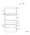
- FIG. 2 Another laser structure 20, according to the present invention, is depicted in Fig. 2.
- the corresponding details are given in the following table: Reference Number of Layer Material Doping Thickness Range Typical Thickness 15.1 Si-wafer - 100 - 1000 ⁇ m ⁇ 300 ⁇ m after polishing 15.4 Ge (pure) - 0.5 - 5 ⁇ m ⁇ 2 ⁇ m 21 GaAs (formed at T s1 ) doped or undoped 1 - 3 nm 2 nm 17 GaAs (formed at T s2 ) doped or undoped 0.2 - 2 ⁇ m ⁇ 0.2 ⁇ m 18 GaAs n + -doped, Si 7 .
- the respective layers of the lasers can be optimized as a function of the emitted power, the number of optical modes wanted, and so forth.
- VCSEL vertical cavity lasers
- a method, according to the present invention, for making an InGaAs/GaAs quantum well laser on a Silicon substrate comprises the following steps:
- the virtual Germanium substrate 15 may comprise a linearly graded Silicon Germanium buffer layer 15.2 with grading rate between 5 and 300%/ ⁇ m.
- This linearly graded Silicon Germanium buffer layer 15.2 is formed underneath the pure Germanium layer 15.3.
- the pure Germanium layer 15.3 serves as cap layer having a thickness between 0.5 ⁇ m and 5 ⁇ m, and preferably about 1 ⁇ m.
- the initial step for the formation of the first Gallium Arsenide layer 16 may be an atomic layer epitaxy step in which case the first Gallium Arsenide layer 16 is an Arsenic/Gallium super-lattice.
- the virtual Germanium substrate 15 may comprise a pure Germanium layer 15.4 being formed directly on the Silicon substrate 15.1.
- the pure Germanium layer 15.4 has a thickness between 0.5 ⁇ m and 5 ⁇ m, and preferably between 1 ⁇ m and 2 ⁇ m.
- the second Gallium Arsenide waveguide layer 17 is undoped and has a thickness between 0.2 - 2 ⁇ m. It may have a thickness of about 1 ⁇ m, for instance.
- the Gallium Arsenide waveguide layer 12 may be undoped. It has a thickness between 0.2 - 0.4 ⁇ m, and preferably about 0.29 ⁇ m.
- the active laser structure comprises an InGaAs quantum well laser structure.
- the active laser structure comprises an InGaAs/AlGaAs/GaAs quantum well laser structure with a compressively strained InGaAs quantum well 11.
- the low-energy plasma-enhanced chemical vapour deposition has a growth rate of up to 10 nm/s.
- the laser structures 10 and 20 are well suited as broad area lasers, for example.
- the laser structures 10 or 20 can be processed as follows to obtain a broad area laser:
- Room temperature amplified spontaneous emission spectra were measured for continuous wave (CW) current injection at a current density of 50 A/cm 2 .
- the spectrum for a laser grown in accordance with the present invention on a VS 15 and an identical reference laser grown on a conventional bulk Ge substrate have been compared.
- the peak wavelength is ⁇ 1.04 ⁇ m for both lasers.
- the optical output power as a function of the drive current has been measured for an InGaAs/GaAs laser grown in accordance with the present invention on a VS 15. This is the first time that laser action at an emission wavelength above 1 ⁇ m has been demonstrated in a strained channel for a structure grown on a SiGe buffer layer 15.2.
- the threshold current amounts to 2 kA/cm 2 .
- An identical reference laser grown on bulk Ge exhibits a threshold current of 500 A/cm 2 .
Landscapes
- Physics & Mathematics (AREA)
- Nanotechnology (AREA)
- Engineering & Computer Science (AREA)
- Chemical & Material Sciences (AREA)
- Optics & Photonics (AREA)
- Biophysics (AREA)
- Life Sciences & Earth Sciences (AREA)
- Electromagnetism (AREA)
- General Physics & Mathematics (AREA)
- Crystallography & Structural Chemistry (AREA)
- Condensed Matter Physics & Semiconductors (AREA)
- Semiconductor Lasers (AREA)
- Recrystallisation Techniques (AREA)
Priority Applications (6)
| Application Number | Priority Date | Filing Date | Title |
|---|---|---|---|
| DE60324425T DE60324425D1 (de) | 2003-09-05 | 2003-09-05 | Durch LEPECVD und MOCVD auf Silizium hergestellte GaAs/GaAs-Laser |
| ES03020169T ES2316680T3 (es) | 2003-09-05 | 2003-09-05 | Laseres de ingaas/gaas sobre silicio producidos mediante lepecvd y mocvd. |
| EP03020169A EP1513233B1 (de) | 2003-09-05 | 2003-09-05 | Durch LEPECVD und MOCVD auf Silizium hergestellte GaAs/GaAs-Laser |
| AT03020169T ATE412999T1 (de) | 2003-09-05 | 2003-09-05 | Durch lepecvd und mocvd auf silizium hergestellte gaas/gaas-laser |
| PCT/EP2004/009873 WO2005025019A1 (en) | 2003-09-05 | 2004-09-04 | InGaAs/GaAs LASERS ON SILICON PRODUCED BY LEPECVD AND MOCVD |
| US10/570,921 US7588954B2 (en) | 2003-09-05 | 2004-09-04 | InGaAs/GaAs lasers on silicon produced by LEPECVD and MOCVD |
Applications Claiming Priority (1)
| Application Number | Priority Date | Filing Date | Title |
|---|---|---|---|
| EP03020169A EP1513233B1 (de) | 2003-09-05 | 2003-09-05 | Durch LEPECVD und MOCVD auf Silizium hergestellte GaAs/GaAs-Laser |
Publications (2)
| Publication Number | Publication Date |
|---|---|
| EP1513233A1 true EP1513233A1 (de) | 2005-03-09 |
| EP1513233B1 EP1513233B1 (de) | 2008-10-29 |
Family
ID=34130149
Family Applications (1)
| Application Number | Title | Priority Date | Filing Date |
|---|---|---|---|
| EP03020169A Expired - Lifetime EP1513233B1 (de) | 2003-09-05 | 2003-09-05 | Durch LEPECVD und MOCVD auf Silizium hergestellte GaAs/GaAs-Laser |
Country Status (6)
| Country | Link |
|---|---|
| US (1) | US7588954B2 (de) |
| EP (1) | EP1513233B1 (de) |
| AT (1) | ATE412999T1 (de) |
| DE (1) | DE60324425D1 (de) |
| ES (1) | ES2316680T3 (de) |
| WO (1) | WO2005025019A1 (de) |
Cited By (3)
| Publication number | Priority date | Publication date | Assignee | Title |
|---|---|---|---|---|
| US8882909B2 (en) | 2004-04-30 | 2014-11-11 | Dichroic Cell S.R.L. | Method for producing virtual Ge substrates for III/V-integration on Si(001) |
| WO2019052672A1 (en) * | 2017-09-18 | 2019-03-21 | Tty-Säätiö Sr. | Semiconductor multilayer structure |
| CN111711063A (zh) * | 2020-06-30 | 2020-09-25 | 度亘激光技术(苏州)有限公司 | 衬底、半导体器件及半导体器件的制作方法 |
Families Citing this family (11)
| Publication number | Priority date | Publication date | Assignee | Title |
|---|---|---|---|---|
| WO2011017773A1 (en) * | 2009-08-13 | 2011-02-17 | Newsouth Innovations Pty Limited | Donor modulation doping of quantum structures |
| CN102570309B (zh) * | 2012-02-14 | 2013-04-17 | 中国科学院半导体研究所 | 采用选区生长有源区的硅基850nm激光器的制备方法 |
| US9407066B2 (en) | 2013-07-24 | 2016-08-02 | GlobalFoundries, Inc. | III-V lasers with integrated silicon photonic circuits |
| CN103579902B (zh) * | 2013-10-25 | 2016-07-13 | 中国科学院半导体研究所 | 一种硅基微腔激光器的制作方法 |
| US9917414B2 (en) | 2015-07-15 | 2018-03-13 | International Business Machines Corporation | Monolithic nanophotonic device on a semiconductor substrate |
| US10122153B2 (en) | 2016-08-29 | 2018-11-06 | International Business Machines Corporation | Resonant cavity strained group III-V photodetector and LED on silicon substrate and method to fabricate same |
| CN106602404A (zh) * | 2016-12-30 | 2017-04-26 | 中国工程物理研究院应用电子学研究所 | 一种半导体激光器及其制作方法 |
| CN108376640A (zh) * | 2018-01-09 | 2018-08-07 | 北京邮电大学 | InGaAs/Si外延材料的制备方法 |
| US11029466B2 (en) * | 2018-11-21 | 2021-06-08 | The Research Foundation For The State University Of New York | Photonics structure with integrated laser |
| CN110165555A (zh) * | 2019-04-28 | 2019-08-23 | 西安理工大学 | 一种基于GexSi1-x可变晶格常数基体的红光半导体激光器 |
| CN121566267A (zh) * | 2026-01-23 | 2026-02-24 | 江西兆驰集成科技有限公司 | 一种硅基磷化铟激光器及其制备方法 |
Citations (1)
| Publication number | Priority date | Publication date | Assignee | Title |
|---|---|---|---|---|
| WO2003044839A2 (en) * | 2001-11-22 | 2003-05-30 | ETH Zürich | Formation of high-mobility silicon-germanium structures by low-energy plasma enhanced chemical vapor deposition |
Family Cites Families (9)
| Publication number | Priority date | Publication date | Assignee | Title |
|---|---|---|---|---|
| EP0988407B9 (de) | 1997-06-13 | 2004-12-15 | Unaxis Trading AG | Verfahren zur herstellung von werkstücken, die mit einer epitaktischen schicht beschichtet sind |
| BR0109069A (pt) * | 2000-03-08 | 2004-12-07 | Ntu Ventures Pte Ltd | Processo para fabricar um circuito integrado fotÈnico |
| AU2003274922A1 (en) * | 2002-08-23 | 2004-03-11 | Amberwave Systems Corporation | Semiconductor heterostructures having reduced dislocation pile-ups and related methods |
| US6841795B2 (en) * | 2002-10-25 | 2005-01-11 | The University Of Connecticut | Semiconductor devices employing at least one modulation doped quantum well structure and one or more etch stop layers for accurate contact formation |
| EP1439570A1 (de) * | 2003-01-14 | 2004-07-21 | Interuniversitair Microelektronica Centrum ( Imec) | Spannungsrelaxierte SiGe Pufferschichten für Anordnungen mit hoher Beweglichkeit und Herstellungsverfahren |
| US7812249B2 (en) * | 2003-04-14 | 2010-10-12 | The Boeing Company | Multijunction photovoltaic cell grown on high-miscut-angle substrate |
| PT1745165E (pt) * | 2004-04-30 | 2011-06-30 | Dichroic Cell S R L | Método para produzir substratos virtuais de ge para integração de iii/v sobre si(001) |
| US20060157732A1 (en) * | 2004-11-09 | 2006-07-20 | Epispeed Sa | Fabrication of MOS-gated strained-Si and SiGe buried channel field effect transistors |
| SG160345A1 (en) * | 2005-02-28 | 2010-04-29 | Epispeed S A | System and process for high-density,low-energy plasma enhanced vapor phase epitaxy |
-
2003
- 2003-09-05 DE DE60324425T patent/DE60324425D1/de not_active Expired - Lifetime
- 2003-09-05 EP EP03020169A patent/EP1513233B1/de not_active Expired - Lifetime
- 2003-09-05 AT AT03020169T patent/ATE412999T1/de active
- 2003-09-05 ES ES03020169T patent/ES2316680T3/es not_active Expired - Lifetime
-
2004
- 2004-09-04 US US10/570,921 patent/US7588954B2/en not_active Expired - Fee Related
- 2004-09-04 WO PCT/EP2004/009873 patent/WO2005025019A1/en not_active Ceased
Patent Citations (1)
| Publication number | Priority date | Publication date | Assignee | Title |
|---|---|---|---|---|
| WO2003044839A2 (en) * | 2001-11-22 | 2003-05-30 | ETH Zürich | Formation of high-mobility silicon-germanium structures by low-energy plasma enhanced chemical vapor deposition |
Non-Patent Citations (2)
| Title |
|---|
| GROENERT M E ET AL: "Improved room-temperature continuous wave GaAs/AlGaAs and InGaAs/GaAs/AlGaAs lasers fabricated on Si substrates via relaxed graded Ge/sub x/Si/sub 1-x/ buffer layers", JOURNAL OF VACUUM SCIENCE & TECHNOLOGY B (MICROELECTRONICS AND NANOMETER STRUCTURES), MAY 2003, AIP FOR AMERICAN VACUUM SOC, USA, vol. 21, no. 3, pages 1064 - 1069, XP002269013, ISSN: 0734-211X * |
| YANG V K ET AL: "Comparison of luminescent efficiency of InGaAs quantum well structures grown on Si, GaAs, Ge, and SiGe virtual substrate", JOURNAL OF APPLIED PHYSICS, 1 MAY 2003, AIP, USA, vol. 93, no. 9, pages 5095 - 5102, XP002269012, ISSN: 0021-8979 * |
Cited By (4)
| Publication number | Priority date | Publication date | Assignee | Title |
|---|---|---|---|---|
| US8882909B2 (en) | 2004-04-30 | 2014-11-11 | Dichroic Cell S.R.L. | Method for producing virtual Ge substrates for III/V-integration on Si(001) |
| WO2019052672A1 (en) * | 2017-09-18 | 2019-03-21 | Tty-Säätiö Sr. | Semiconductor multilayer structure |
| US11688996B2 (en) | 2017-09-18 | 2023-06-27 | Tampere University Foundation, sr. | Semiconductor multilayer structure |
| CN111711063A (zh) * | 2020-06-30 | 2020-09-25 | 度亘激光技术(苏州)有限公司 | 衬底、半导体器件及半导体器件的制作方法 |
Also Published As
| Publication number | Publication date |
|---|---|
| US7588954B2 (en) | 2009-09-15 |
| ES2316680T3 (es) | 2009-04-16 |
| ATE412999T1 (de) | 2008-11-15 |
| WO2005025019A1 (en) | 2005-03-17 |
| DE60324425D1 (de) | 2008-12-11 |
| EP1513233B1 (de) | 2008-10-29 |
| US20070164311A1 (en) | 2007-07-19 |
Similar Documents
| Publication | Publication Date | Title |
|---|---|---|
| US5937274A (en) | Fabrication method for AlGaIn NPAsSb based devices | |
| US4876219A (en) | Method of forming a heteroepitaxial semiconductor thin film using amorphous buffer layers | |
| US5679152A (en) | Method of making a single crystals Ga*N article | |
| US6372356B1 (en) | Compliant substrates for growing lattice mismatched films | |
| US5838029A (en) | GaN-type light emitting device formed on a silicon substrate | |
| EP2383846B1 (de) | Lichtemissionsvorrichtung und Herstellungsverfahren dafür | |
| KR100623558B1 (ko) | Iii족 질화물계 화합물 반도체 및 그 제조방법 | |
| US10825912B2 (en) | Integrated epitaxial metal electrodes | |
| US7588954B2 (en) | InGaAs/GaAs lasers on silicon produced by LEPECVD and MOCVD | |
| KR20120025369A (ko) | 질화물 반도체 결정층을 제조하기 위한 방법 | |
| US20220006264A1 (en) | Semiconductor device and fabrication method | |
| US20070160100A1 (en) | Misfit dislocation forming interfacial self-assembly for growth of highly-mismatched III-Sb alloys | |
| US20010016404A1 (en) | GaN substrate including wide low - defect region for use in semiconductor element | |
| KR20010090165A (ko) | 이종접합구조의 양자점 버퍼층을 가지는 반도체 소자 | |
| US9401404B2 (en) | Semiconductor device and fabrication method | |
| US10418457B2 (en) | Metal electrode with tunable work functions | |
| US5571748A (en) | Methods for producing compound semiconductor devices | |
| EP2438663B1 (de) | Laserdiode und verfahren zur herstellung der laserdiode | |
| EP3915133A1 (de) | Integrierte epitaktische metallelektroden | |
| JPH03297186A (ja) | 半導体装置及びその製造法 | |
| WO2025261641A1 (en) | Semiconductor structures | |
| Modak et al. | 5.2% efficiency lnAlGaP microcavity LEDs at | |
| Egawa et al. | Characterization of single quantum wells on GaAs/Si grown by metalorganic chemical vapor deposition | |
| Groenert et al. | Strategies for Direct Monolithic Integration of AlxGa (1-x) As/InxGa (1-x) As LEDS and Lasers on Ge/GeSi/Si Substrates Via Relaxed Graded GexSi (1-x) Buffer Layers | |
| JP2002016320A (ja) | 化合物半導体装置およびその製造方法 |
Legal Events
| Date | Code | Title | Description |
|---|---|---|---|
| PUAI | Public reference made under article 153(3) epc to a published international application that has entered the european phase |
Free format text: ORIGINAL CODE: 0009012 |
|
| AK | Designated contracting states |
Kind code of ref document: A1 Designated state(s): AT BE BG CH CY CZ DE DK EE ES FI FR GB GR HU IE IT LI LU MC NL PT RO SE SI SK TR |
|
| AX | Request for extension of the european patent |
Extension state: AL LT LV MK |
|
| 17P | Request for examination filed |
Effective date: 20050711 |
|
| AKX | Designation fees paid |
Designated state(s): AT BE BG CH CY CZ DE DK EE ES FI FR GB GR HU IE IT LI LU MC NL PT RO SE SI SK TR |
|
| RAP1 | Party data changed (applicant data changed or rights of an application transferred) |
Owner name: EPISPEED S.A. |
|
| GRAP | Despatch of communication of intention to grant a patent |
Free format text: ORIGINAL CODE: EPIDOSNIGR1 |
|
| GRAS | Grant fee paid |
Free format text: ORIGINAL CODE: EPIDOSNIGR3 |
|
| GRAA | (expected) grant |
Free format text: ORIGINAL CODE: 0009210 |
|
| AK | Designated contracting states |
Kind code of ref document: B1 Designated state(s): AT BE BG CH CY CZ DE DK EE ES FI FR GB GR HU IE IT LI LU MC NL PT RO SE SI SK TR |
|
| REG | Reference to a national code |
Ref country code: GB Ref legal event code: FG4D |
|
| REG | Reference to a national code |
Ref country code: CH Ref legal event code: EP |
|
| REG | Reference to a national code |
Ref country code: IE Ref legal event code: FG4D |
|
| REF | Corresponds to: |
Ref document number: 60324425 Country of ref document: DE Date of ref document: 20081211 Kind code of ref document: P |
|
| REG | Reference to a national code |
Ref country code: CH Ref legal event code: NV Representative=s name: OK PAT AG PATENTE MARKEN LIZENZEN |
|
| NLV1 | Nl: lapsed or annulled due to failure to fulfill the requirements of art. 29p and 29m of the patents act | ||
| REG | Reference to a national code |
Ref country code: ES Ref legal event code: FG2A Ref document number: 2316680 Country of ref document: ES Kind code of ref document: T3 |
|
| PG25 | Lapsed in a contracting state [announced via postgrant information from national office to epo] |
Ref country code: BG Free format text: LAPSE BECAUSE OF FAILURE TO SUBMIT A TRANSLATION OF THE DESCRIPTION OR TO PAY THE FEE WITHIN THE PRESCRIBED TIME-LIMIT Effective date: 20090129 |
|
| PG25 | Lapsed in a contracting state [announced via postgrant information from national office to epo] |
Ref country code: FI Free format text: LAPSE BECAUSE OF FAILURE TO SUBMIT A TRANSLATION OF THE DESCRIPTION OR TO PAY THE FEE WITHIN THE PRESCRIBED TIME-LIMIT Effective date: 20081029 Ref country code: NL Free format text: LAPSE BECAUSE OF FAILURE TO SUBMIT A TRANSLATION OF THE DESCRIPTION OR TO PAY THE FEE WITHIN THE PRESCRIBED TIME-LIMIT Effective date: 20081029 Ref country code: SI Free format text: LAPSE BECAUSE OF FAILURE TO SUBMIT A TRANSLATION OF THE DESCRIPTION OR TO PAY THE FEE WITHIN THE PRESCRIBED TIME-LIMIT Effective date: 20081029 Ref country code: PT Free format text: LAPSE BECAUSE OF FAILURE TO SUBMIT A TRANSLATION OF THE DESCRIPTION OR TO PAY THE FEE WITHIN THE PRESCRIBED TIME-LIMIT Effective date: 20090330 |
|
| PG25 | Lapsed in a contracting state [announced via postgrant information from national office to epo] |
Ref country code: BE Free format text: LAPSE BECAUSE OF FAILURE TO SUBMIT A TRANSLATION OF THE DESCRIPTION OR TO PAY THE FEE WITHIN THE PRESCRIBED TIME-LIMIT Effective date: 20081029 Ref country code: EE Free format text: LAPSE BECAUSE OF FAILURE TO SUBMIT A TRANSLATION OF THE DESCRIPTION OR TO PAY THE FEE WITHIN THE PRESCRIBED TIME-LIMIT Effective date: 20081029 Ref country code: DK Free format text: LAPSE BECAUSE OF FAILURE TO SUBMIT A TRANSLATION OF THE DESCRIPTION OR TO PAY THE FEE WITHIN THE PRESCRIBED TIME-LIMIT Effective date: 20081029 Ref country code: RO Free format text: LAPSE BECAUSE OF FAILURE TO SUBMIT A TRANSLATION OF THE DESCRIPTION OR TO PAY THE FEE WITHIN THE PRESCRIBED TIME-LIMIT Effective date: 20081029 |
|
| PG25 | Lapsed in a contracting state [announced via postgrant information from national office to epo] |
Ref country code: SE Free format text: LAPSE BECAUSE OF FAILURE TO SUBMIT A TRANSLATION OF THE DESCRIPTION OR TO PAY THE FEE WITHIN THE PRESCRIBED TIME-LIMIT Effective date: 20090129 Ref country code: CZ Free format text: LAPSE BECAUSE OF FAILURE TO SUBMIT A TRANSLATION OF THE DESCRIPTION OR TO PAY THE FEE WITHIN THE PRESCRIBED TIME-LIMIT Effective date: 20081029 |
|
| PLBE | No opposition filed within time limit |
Free format text: ORIGINAL CODE: 0009261 |
|
| STAA | Information on the status of an ep patent application or granted ep patent |
Free format text: STATUS: NO OPPOSITION FILED WITHIN TIME LIMIT |
|
| PG25 | Lapsed in a contracting state [announced via postgrant information from national office to epo] |
Ref country code: SK Free format text: LAPSE BECAUSE OF FAILURE TO SUBMIT A TRANSLATION OF THE DESCRIPTION OR TO PAY THE FEE WITHIN THE PRESCRIBED TIME-LIMIT Effective date: 20081029 |
|
| 26N | No opposition filed |
Effective date: 20090730 |
|
| PG25 | Lapsed in a contracting state [announced via postgrant information from national office to epo] |
Ref country code: MC Free format text: LAPSE BECAUSE OF NON-PAYMENT OF DUE FEES Effective date: 20090930 |
|
| REG | Reference to a national code |
Ref country code: IE Ref legal event code: MM4A |
|
| PG25 | Lapsed in a contracting state [announced via postgrant information from national office to epo] |
Ref country code: IE Free format text: LAPSE BECAUSE OF NON-PAYMENT OF DUE FEES Effective date: 20090905 |
|
| PG25 | Lapsed in a contracting state [announced via postgrant information from national office to epo] |
Ref country code: GR Free format text: LAPSE BECAUSE OF FAILURE TO SUBMIT A TRANSLATION OF THE DESCRIPTION OR TO PAY THE FEE WITHIN THE PRESCRIBED TIME-LIMIT Effective date: 20090130 |
|
| PG25 | Lapsed in a contracting state [announced via postgrant information from national office to epo] |
Ref country code: LU Free format text: LAPSE BECAUSE OF NON-PAYMENT OF DUE FEES Effective date: 20090905 |
|
| PG25 | Lapsed in a contracting state [announced via postgrant information from national office to epo] |
Ref country code: HU Free format text: LAPSE BECAUSE OF FAILURE TO SUBMIT A TRANSLATION OF THE DESCRIPTION OR TO PAY THE FEE WITHIN THE PRESCRIBED TIME-LIMIT Effective date: 20090430 |
|
| PG25 | Lapsed in a contracting state [announced via postgrant information from national office to epo] |
Ref country code: TR Free format text: LAPSE BECAUSE OF FAILURE TO SUBMIT A TRANSLATION OF THE DESCRIPTION OR TO PAY THE FEE WITHIN THE PRESCRIBED TIME-LIMIT Effective date: 20081029 |
|
| PG25 | Lapsed in a contracting state [announced via postgrant information from national office to epo] |
Ref country code: CY Free format text: LAPSE BECAUSE OF FAILURE TO SUBMIT A TRANSLATION OF THE DESCRIPTION OR TO PAY THE FEE WITHIN THE PRESCRIBED TIME-LIMIT Effective date: 20081029 |
|
| PGFP | Annual fee paid to national office [announced via postgrant information from national office to epo] |
Ref country code: CH Payment date: 20140929 Year of fee payment: 12 |
|
| PGFP | Annual fee paid to national office [announced via postgrant information from national office to epo] |
Ref country code: ES Payment date: 20140926 Year of fee payment: 12 Ref country code: GB Payment date: 20140929 Year of fee payment: 12 Ref country code: FR Payment date: 20140917 Year of fee payment: 12 Ref country code: AT Payment date: 20140820 Year of fee payment: 12 |
|
| PGFP | Annual fee paid to national office [announced via postgrant information from national office to epo] |
Ref country code: DE Payment date: 20140929 Year of fee payment: 12 |
|
| PGFP | Annual fee paid to national office [announced via postgrant information from national office to epo] |
Ref country code: IT Payment date: 20140929 Year of fee payment: 12 |
|
| REG | Reference to a national code |
Ref country code: DE Ref legal event code: R119 Ref document number: 60324425 Country of ref document: DE |
|
| PG25 | Lapsed in a contracting state [announced via postgrant information from national office to epo] |
Ref country code: IT Free format text: LAPSE BECAUSE OF NON-PAYMENT OF DUE FEES Effective date: 20150905 |
|
| REG | Reference to a national code |
Ref country code: CH Ref legal event code: PL |
|
| REG | Reference to a national code |
Ref country code: AT Ref legal event code: MM01 Ref document number: 412999 Country of ref document: AT Kind code of ref document: T Effective date: 20150905 |
|
| GBPC | Gb: european patent ceased through non-payment of renewal fee |
Effective date: 20150905 |
|
| REG | Reference to a national code |
Ref country code: FR Ref legal event code: ST Effective date: 20160531 |
|
| PG25 | Lapsed in a contracting state [announced via postgrant information from national office to epo] |
Ref country code: DE Free format text: LAPSE BECAUSE OF NON-PAYMENT OF DUE FEES Effective date: 20160401 Ref country code: GB Free format text: LAPSE BECAUSE OF NON-PAYMENT OF DUE FEES Effective date: 20150905 Ref country code: LI Free format text: LAPSE BECAUSE OF NON-PAYMENT OF DUE FEES Effective date: 20150930 Ref country code: CH Free format text: LAPSE BECAUSE OF NON-PAYMENT OF DUE FEES Effective date: 20150930 |
|
| PG25 | Lapsed in a contracting state [announced via postgrant information from national office to epo] |
Ref country code: FR Free format text: LAPSE BECAUSE OF NON-PAYMENT OF DUE FEES Effective date: 20150930 Ref country code: AT Free format text: LAPSE BECAUSE OF NON-PAYMENT OF DUE FEES Effective date: 20150905 |
|
| REG | Reference to a national code |
Ref country code: ES Ref legal event code: FD2A Effective date: 20161026 |
|
| PG25 | Lapsed in a contracting state [announced via postgrant information from national office to epo] |
Ref country code: ES Free format text: LAPSE BECAUSE OF NON-PAYMENT OF DUE FEES Effective date: 20150906 |