EP1513072A2 - Méthode d'ordonnancement de mémoire multi-banc - Google Patents
Méthode d'ordonnancement de mémoire multi-banc Download PDFInfo
- Publication number
- EP1513072A2 EP1513072A2 EP04300399A EP04300399A EP1513072A2 EP 1513072 A2 EP1513072 A2 EP 1513072A2 EP 04300399 A EP04300399 A EP 04300399A EP 04300399 A EP04300399 A EP 04300399A EP 1513072 A2 EP1513072 A2 EP 1513072A2
- Authority
- EP
- European Patent Office
- Prior art keywords
- bank
- input stream
- writing
- banks
- stream
- Prior art date
- Legal status (The legal status is an assumption and is not a legal conclusion. Google has not performed a legal analysis and makes no representation as to the accuracy of the status listed.)
- Withdrawn
Links
Images

Classifications
-
- G—PHYSICS
- G06—COMPUTING OR CALCULATING; COUNTING
- G06F—ELECTRIC DIGITAL DATA PROCESSING
- G06F13/00—Interconnection of, or transfer of information or other signals between, memories, input/output devices or central processing units
- G06F13/14—Handling requests for interconnection or transfer
- G06F13/16—Handling requests for interconnection or transfer for access to memory bus
- G06F13/1605—Handling requests for interconnection or transfer for access to memory bus based on arbitration
- G06F13/1647—Handling requests for interconnection or transfer for access to memory bus based on arbitration with interleaved bank access
-
- G—PHYSICS
- G11—INFORMATION STORAGE
- G11C—STATIC STORES
- G11C7/00—Arrangements for writing information into, or reading information out from, a digital store
- G11C7/10—Input/output [I/O] data interface arrangements, e.g. I/O data control circuits, I/O data buffers
- G11C7/1015—Read-write modes for single port memories, i.e. having either a random port or a serial port
- G11C7/1042—Read-write modes for single port memories, i.e. having either a random port or a serial port using interleaving techniques, i.e. read-write of one part of the memory while preparing another part
Definitions
- the present invention relates to a method for scheduling and controlling access to a multibank memory, and to an apparatus for reading from and/or writing to recording media using such method.
- SDRAM synchronous dynamical random access memory
- DDR-RAM double data rate RAM
- ESDRAM enhanced synchronous DRAM
- SLDRAM synchronous link DRAM
- RDRAM Rambus DRAM
- SRAM single-port static random access memory
- Typical SDRAM modules comprise four independent banks. Each bank consists of rows, which consist of columns. To access a datum the corresponding row on the corresponding bank is opened by the command 'activate' for reading and writing. After activation, which needs 2 to 4 cycles, the data transfer is initiated by sending a 'read' or 'write' command together with the column address. After the transfer the bank is precharged, which again needs 2 to 4 cycles, to deactivate the open row and to prepare the bank for the next 'activate' command. The command 'precharge' closes the open row.
- a burst transfer is used for reading or writing several data with only one 'read' or 'write' command.
- the access starts at a selected location (column) and continues for a programmed number of locations. After initiating a new burst, the command bus is free and can be used to activate or precharge other banks.
- SDRAM is used for simultaneously storing CPU-instructions as well as data.
- the SDRAM is accessed through a cache.
- a linear access is achieved in the following way: first bank first row, second bank first row, third bank first row, fourth bank first row, first bank second row and so on. Assuming a linear access this allows to hide latency by activating the row on the next bank before the CPU/cache actually wants to access this row.
- a single SDRAM module is favorably used for storing instructions and data for an on-chip-CPU and for buffering the real-time data stream between a drive for the recording media and a host.
- the burst length of the buffer input and output stream need to be reduced to only a few beats.
- the overhead caused by the four interfaces, i.e. CPU-instructions, CPU-data, input stream, and output stream acts like random access.
- read and write access to the buffer is in random order. Therefore, since the next row is unknown, pre-activation of buffer banks is not possible.
- the SDRAM module can be replaced by static RAM (SPAM).
- the number of modules can be increased for reducing the workload of a single module, or the width of the data bus between the module and the application specific integrated circuit (ASIC) can be expanded for increasing the bandwidth.
- a further solution consists in de-coupling the buffer input and output, which can be performed by large on-chip SRAM buffering two or more complete rows. However, in this case a very complex logic is required for controlling the data flow.
- a method for controlling access to a multibank memory having at least two banks comprises the steps of:
- the method further comprises the steps of:
- the method further comprises the steps of:
- the method further comprises the steps of:
- the multibank memory is a dynamical random access memory, e.g. an SDRAM.
- the method according to the invention takes full advantage of the pipelining architecture of the memory.
- the method further comprises the step of holding an activated row of a bank open until a refresh cycle is issued or until the end of the row is reached by a burst. This allows to save approximately ten cycles latency for each single access.
- the banks are single-port static random access memory modules.
- input data are written into the first module until a read request is received for this module.
- the input data are then written into the second module whilst data are read from the first module. Reading and writing is, therefore, performed simultaneously.
- a further advantage is that instead of a more expensive and complicated dual-port SRAM module of a specific size two single-port SRAM modules with half the size each can be used, e.g. two single-port SRAM modules with 512 bytes each instead of a dual-port SRAM module with 1024 bytes.
- more than two banks are provided for data buffering. This allows to buffer a larger amount of data. However, the overall performance is not further enhanced by this measure.
- the method further comprises the steps of:
- a device for controlling access to a multibank memory having at least two banks performs a method according to the invention.
- an apparatus for reading from and/or writing to recording media uses a method or comprises a device according to the invention for controlling access to a multibank memory having at least two banks.
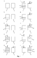
- Fig. 1 access to two banks 1,2 of an SDRAM using a method according to the invention is shown.
- the access is divided into a sequence of states of the banks, which are depicted in parts a) to j) of Fig. 1.
- a single complete output block is written into one bank 1,2.
- a plurality of output blocks can subsequently be written into the banks.
- both banks 1,2 are empty, which corresponds to Fig. 1a).
- a pointer 5 is set to mark the size of an output block.
- the input stream 6 coming from the drive are now stored in the left bank 1, which is depicted in part c). As soon as the pointer 5 is reached, the buffer can be read.
- the writing to the left bank 1 continues. This is shown in part d).
- the first bank 1 is filled with a plurality of output blocks.
- the input stream 6 is switched to the right bank 2 and its last position on the left bank 1 is marked with a further pointer 7, which is depicted in part e).
- the input stream 6 and the output stream 8 are active at the same time until the complete output block size has been read from the left bank 1.
- a new pointer 9 is set marking the size of an output block, which is shown in part h). When this pointer 9 is reached, the left bank 1 is read until the jump point 7 is reached.
- the access scheme can be extended to more than two banks. In this case upon switching between the banks it is possible to choose among at least two banks for writing the imput stream. By way of example, this choice can be based on the overall workload of each bank.
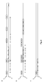
- Latencies during data transfer on an SDRAM bank 1, 2 are shown in Fig. 2.
- the data transfer is divided into data transfer occurring on a command bus 3 and data transfer occurring on a data bus 4.
- Fig. 2a depicts a typical random read/write access to one SDRAM bank only. First a row from that bank is activated. Then a write command to that row is issued and the data transfer is initiated. After that a precharge command is given for closing the row and for precharging for the next row access. Another row on the same bank is then activated, a read command to that row is issued and data transfer starts after a delay due to the 'read' command.
- FIG. 2b An SDRAM access over more than one bank is shown in Fig. 2b).
- First a row from a first bank is activated.
- a write command to that row from the first bank is then issued and data transfer is initiated.
- Simultaneously a row from a second bank is activated.
- a read command to that row from the second bank is then given and data transfer starts after a delay due to the 'read' command. It is to be noted that a write command in this example would lead to a data transfer from the second bank directly concatenated to the data transfer of the first bank.
- Fig. 2c shows a single burst to an already opened row on the same bank. In this case a write command is each time processed without delay on that row.
- FIG. 3 an apparatus for reading from recording media 20, e.g. optical recording media, using a method according to the invention is shown.
- Data are read from the recording medium 20 and are pre-processed by a pre-processing block 21, e.g. for error correction.
- the pre-processed data are transmitted as an input stream via a first interface 23 to an integrated circuit 22, which among other functions controls the data transfer within the apparatus.
- the integrated circuit 22 Via a second interface 24 the integrated circuit 22 communicates with a data bus 28, e.g. an ATA bus. Using this data bus 28 requested data are output for further processing.
- a micro-controller 29 communicates with the integrated circuit 22 via a third interface 25, e.g. for controlling settings of the integrated circuit 22 or for requesting specific data.
- the integrated circuit comprises an internal buffer 26 comprising a plurality of SDRAM banks 1, 2 for buffering all incoming data.
- the data traffic is controlled by a scheduler 27, which performs the method described with reference to Fig. 1 for handling the buffer accesses.
- the input stream and the output stream are physically separated from instructions from the micro-controller 29 and micro-controller data.
Landscapes
- Engineering & Computer Science (AREA)
- Theoretical Computer Science (AREA)
- Physics & Mathematics (AREA)
- General Engineering & Computer Science (AREA)
- General Physics & Mathematics (AREA)
- Dram (AREA)
- Signal Processing For Digital Recording And Reproducing (AREA)
Priority Applications (1)
| Application Number | Priority Date | Filing Date | Title |
|---|---|---|---|
| EP04300399A EP1513072A3 (fr) | 2003-09-02 | 2004-06-28 | Méthode d'ordonnancement de mémoire multi-banc |
Applications Claiming Priority (3)
| Application Number | Priority Date | Filing Date | Title |
|---|---|---|---|
| EP03019948A EP1513157A1 (fr) | 2003-09-02 | 2003-09-02 | Procédé d'accès dans une memoire multi-bancs |
| EP03019948 | 2003-09-02 | ||
| EP04300399A EP1513072A3 (fr) | 2003-09-02 | 2004-06-28 | Méthode d'ordonnancement de mémoire multi-banc |
Publications (2)
| Publication Number | Publication Date |
|---|---|
| EP1513072A2 true EP1513072A2 (fr) | 2005-03-09 |
| EP1513072A3 EP1513072A3 (fr) | 2009-10-21 |
Family
ID=34137570
Family Applications (1)
| Application Number | Title | Priority Date | Filing Date |
|---|---|---|---|
| EP04300399A Withdrawn EP1513072A3 (fr) | 2003-09-02 | 2004-06-28 | Méthode d'ordonnancement de mémoire multi-banc |
Country Status (1)
| Country | Link |
|---|---|
| EP (1) | EP1513072A3 (fr) |
Cited By (1)
| Publication number | Priority date | Publication date | Assignee | Title |
|---|---|---|---|---|
| EP2323099A1 (fr) * | 2009-10-23 | 2011-05-18 | Seiko Epson Corporation | Dispositif de lecture d'images et procédé d'écriture de données images dans un dispositif de lecture d'images |
Family Cites Families (4)
| Publication number | Priority date | Publication date | Assignee | Title |
|---|---|---|---|---|
| US5732041A (en) * | 1993-08-19 | 1998-03-24 | Mmc Networks, Inc. | Memory interface unit, shared memory switch system and associated method |
| US5881016A (en) * | 1997-06-13 | 1999-03-09 | Cirrus Logic, Inc. | Method and apparatus for optimizing power consumption and memory bandwidth in a video controller using SGRAM and SDRAM power reduction modes |
| GB2381103B (en) * | 1997-12-17 | 2003-06-04 | Fujitsu Ltd | Memory access methods and devices for use with random access memories |
| JP2000315173A (ja) * | 1999-04-30 | 2000-11-14 | Matsushita Electric Ind Co Ltd | メモリ制御装置 |
-
2004
- 2004-06-28 EP EP04300399A patent/EP1513072A3/fr not_active Withdrawn
Cited By (1)
| Publication number | Priority date | Publication date | Assignee | Title |
|---|---|---|---|---|
| EP2323099A1 (fr) * | 2009-10-23 | 2011-05-18 | Seiko Epson Corporation | Dispositif de lecture d'images et procédé d'écriture de données images dans un dispositif de lecture d'images |
Also Published As
| Publication number | Publication date |
|---|---|
| EP1513072A3 (fr) | 2009-10-21 |
Similar Documents
| Publication | Publication Date | Title |
|---|---|---|
| EP1488323B1 (fr) | Systeme memoire a duree des rafales inferieure a la duree de prelecture | |
| EP1474747B1 (fr) | Espace d'adresse, systeme de bus, controleur de memoire et systeme de dispositifs | |
| KR101622311B1 (ko) | 적응가능한 수의 오픈 로우들을 갖는 메모리 디바이스 | |
| US20040228166A1 (en) | Buffer chip and method for actuating one or more memory arrangements | |
| US20060168407A1 (en) | Memory hub system and method having large virtual page size | |
| US7277996B2 (en) | Modified persistent auto precharge command protocol system and method for memory devices | |
| KR20080104184A (ko) | 모드-선택 프리페치 및 클록-코어 타이밍 기능을 갖는 메모리장치 | |
| JP2008532140A (ja) | 複数内部データバス及びメモリバンクインターリービングを有するメモリデバイス及び方法 | |
| WO2003098392A2 (fr) | Sequenceur dram a remaniement d'ordre | |
| JP4704345B2 (ja) | 暗示dramプレチャージ用の方法及びデバイス | |
| CN1630858A (zh) | 用于计算机系统中的辅助命令总线的方法和设备 | |
| US6922770B2 (en) | Memory controller providing dynamic arbitration of memory commands | |
| KR100873829B1 (ko) | 단방향 데이터 버스를 가진 메모리 시스템 및 방법 | |
| US7613866B2 (en) | Method for controlling access to a multibank memory | |
| CN101042926A (zh) | 存储器控制方法,存储装置以及存储器控制器 | |
| KR101645003B1 (ko) | 메모리 제어기 및 그 메모리 제어기가 탑재된 컴퓨팅 장치 | |
| KR100438736B1 (ko) | 어드레스 라인을 이용해 데이터 쓰기를 수행하는 메모리제어 장치 | |
| CN108027765B (zh) | 一种内存访问方法以及计算机系统 | |
| EP1513072A2 (fr) | Méthode d'ordonnancement de mémoire multi-banc | |
| CN109508305A (zh) | 存储器装置和包括存储器装置的存储器系统 | |
| CN100561593C (zh) | 一种随机存储器的访问方法及装置 | |
| KR100368132B1 (ko) | 메모리 어드레싱 방법 | |
| JP2020087055A (ja) | メモリ制御装置 | |
| HK1068181B (en) | Memory system with burst length shorter than prefetch length | |
| JPH04104638A (ja) | 通信制御システム |
Legal Events
| Date | Code | Title | Description |
|---|---|---|---|
| PUAI | Public reference made under article 153(3) epc to a published international application that has entered the european phase |
Free format text: ORIGINAL CODE: 0009012 |
|
| AK | Designated contracting states |
Kind code of ref document: A2 Designated state(s): AT BE BG CH CY CZ DE DK EE ES FI FR GB GR HU IE IT LI LU MC NL PL PT RO SE SI SK TR |
|
| AX | Request for extension of the european patent |
Extension state: AL HR LT LV MK |
|
| RAP1 | Party data changed (applicant data changed or rights of an application transferred) |
Owner name: THOMSON LICENSING |
|
| PUAL | Search report despatched |
Free format text: ORIGINAL CODE: 0009013 |
|
| AK | Designated contracting states |
Kind code of ref document: A3 Designated state(s): AT BE BG CH CY CZ DE DK EE ES FI FR GB GR HU IE IT LI LU MC NL PL PT RO SE SI SK TR |
|
| AX | Request for extension of the european patent |
Extension state: AL HR LT LV MK |
|
| RIC1 | Information provided on ipc code assigned before grant |
Ipc: G06F 13/16 20060101ALI20090916BHEP Ipc: G06F 12/06 20060101ALI20090916BHEP Ipc: G11C 7/10 20060101AFI20090916BHEP |
|
| RAP1 | Party data changed (applicant data changed or rights of an application transferred) |
Owner name: THOMSON LICENSING |
|
| 17P | Request for examination filed |
Effective date: 20100415 |
|
| AKX | Designation fees paid |
Designated state(s): DE FR GB |
|
| 17Q | First examination report despatched |
Effective date: 20110819 |
|
| STAA | Information on the status of an ep patent application or granted ep patent |
Free format text: STATUS: THE APPLICATION IS DEEMED TO BE WITHDRAWN |
|
| 18D | Application deemed to be withdrawn |
Effective date: 20111230 |