EP1512547A2 - Capteur imprimé - Google Patents
Capteur imprimé Download PDFInfo
- Publication number
- EP1512547A2 EP1512547A2 EP04254760A EP04254760A EP1512547A2 EP 1512547 A2 EP1512547 A2 EP 1512547A2 EP 04254760 A EP04254760 A EP 04254760A EP 04254760 A EP04254760 A EP 04254760A EP 1512547 A2 EP1512547 A2 EP 1512547A2
- Authority
- EP
- European Patent Office
- Prior art keywords
- substrate
- sensor
- electroconductive
- contact
- elements
- Prior art date
- Legal status (The legal status is an assumption and is not a legal conclusion. Google has not performed a legal analysis and makes no representation as to the accuracy of the status listed.)
- Withdrawn
Links
Images


Classifications
-
- H—ELECTRICITY
- H01—ELECTRIC ELEMENTS
- H01H—ELECTRIC SWITCHES; RELAYS; SELECTORS; EMERGENCY PROTECTIVE DEVICES
- H01H1/00—Contacts
- H01H1/12—Contacts characterised by the manner in which co-operating contacts engage
- H01H1/36—Contacts characterised by the manner in which co-operating contacts engage by sliding
- H01H1/40—Contact mounted so that its contact-making surface is flush with adjoining insulation
- H01H1/403—Contacts forming part of a printed circuit
-
- B—PERFORMING OPERATIONS; TRANSPORTING
- B42—BOOKBINDING; ALBUMS; FILES; SPECIAL PRINTED MATTER
- B42D—BOOKS; BOOK COVERS; LOOSE LEAVES; PRINTED MATTER CHARACTERISED BY IDENTIFICATION OR SECURITY FEATURES; PRINTED MATTER OF SPECIAL FORMAT OR STYLE NOT OTHERWISE PROVIDED FOR; DEVICES FOR USE THEREWITH AND NOT OTHERWISE PROVIDED FOR; MOVABLE-STRIP WRITING OR READING APPARATUS
- B42D15/00—Printed matter of special format or style not otherwise provided for
- B42D15/02—Postcards; Greeting, menu, business or like cards; Letter cards or letter-sheets
- B42D15/022—Postcards; Greeting, menu, business or like cards; Letter cards or letter-sheets combined with permanently fastened sound-producing or light-emitting means or carrying sound records
-
- B—PERFORMING OPERATIONS; TRANSPORTING
- B42—BOOKBINDING; ALBUMS; FILES; SPECIAL PRINTED MATTER
- B42D—BOOKS; BOOK COVERS; LOOSE LEAVES; PRINTED MATTER CHARACTERISED BY IDENTIFICATION OR SECURITY FEATURES; PRINTED MATTER OF SPECIAL FORMAT OR STYLE NOT OTHERWISE PROVIDED FOR; DEVICES FOR USE THEREWITH AND NOT OTHERWISE PROVIDED FOR; MOVABLE-STRIP WRITING OR READING APPARATUS
- B42D3/00—Book covers
- B42D3/12—Book covers combined with other articles
-
- H—ELECTRICITY
- H01—ELECTRIC ELEMENTS
- H01H—ELECTRIC SWITCHES; RELAYS; SELECTORS; EMERGENCY PROTECTIVE DEVICES
- H01H2201/00—Contacts
- H01H2201/018—Contacts transparent
-
- H—ELECTRICITY
- H03—ELECTRONIC CIRCUITRY
- H03K—PULSE TECHNIQUE
- H03K17/00—Electronic switching or gating, i.e. not by contact-making and –breaking
- H03K17/94—Electronic switching or gating, i.e. not by contact-making and –breaking characterised by the way in which the control signals are generated
- H03K17/965—Switches controlled by moving an element forming part of the switch
- H03K17/975—Switches controlled by moving an element forming part of the switch using a capacitive movable element
Definitions
- the present invention relates to a sensor and to sensor devices that can be employed in electronic circuits, particularly printed electronic circuits. More particularly, the embodiments disclosed relate to sensors or switch mechanisms that can be employed in devices including print media.
- Electronic enhancements have been suggested for a variety of print media devices such as books, greeting cards and the like.
- the electronic enhancements suggested are used to provide visual enhancement or interest to printed material such as by animating text or graphic images.
- Electronically enhanced print media often employ mechanical switches or other mechanical devices in order to initiate the playback of sounds or performance of other electronic features. Such mechanically based switches are resource and space intensive. Thus, alternate switching and sensor mechanisms for use in conjunction with print media or various other applications where resource usage and/or space constraints could be desirable.
- a sensor/switching device configuration that includes a substrate and at least one element imprinted on the substrate which contains an electroconductive material.
- the element includes at least one active region surface configured in at least one of conductive mode, inductive mode, and capacitative mode and have at least one electroconductive material-containing element.
- the electroconductive material is usually indiscernible from the substrate.
- a sensor/switching device configuration that can be employed on and with various substrate materials.
- the sensor configuration can be employed in conjunction with suitable media such as print media.
- suitable media such as print media.
- the print media may be interactive and/or electronically augmented or visually enhanced. It is also contemplated that the sensor/switching device configuration can be employed with other devices for which invisibility, or visual indistinctiveness is desired or required.
- a sensor/switching device mechanism that includes a substrate and at least one element imprinted on the substrate.
- the imprinted element contains electroconductive material.
- substrate is taken to mean any solid material capable of receiving and maintaining a printed layer thereon. Materials of choice will be essentially non-conducting or will be capable of being rendered sufficiently insulative to permit the suitable function of electroconductive materials included in the imprinted layer.
- Suitable substrate materials can be flexible or rigid depending upon the end use to which the substrate material and associated printed material is to be put. Non-limiting examples of flexible materials include various grades and types of paper and paper products as well as plastics, plastic laminates and the like.
- Non-limiting examples of rigid substrates include wood, plastic structural material and the like.
- electroconductive material is taken to mean a material capable of conducting or transferring at least a quantity of electrical charge sufficient to operate a power drawing device associated or connected with the sensor/switch or capable of being rendered so.
- imprinted as defined herein is taken to mean positioned on the substrate by means of a suitable deposition process such as by fluid jet deposition, and the like.
- Suitable electroconductive materials include, but are not limited to materials such as organic or inorganic materials or materials which can be rendered conductive by doping or by other processing applications or procedures and other electroconductive materials which can be deposited in similar manners.
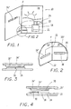
- FIG. 1 there is depicted an animated greeting card 10 having a sensor/switching device 12 as disclosed herein.
- the greeting card 10 is considered as exemplary of the type of device or element which can utilize the sensor/switching device 12 as disclosed herein.
- the sensor/switching device may be used on other devices or apparatus having at least one substrate surface.
- the sensor/switching device 12 includes a substrate 14 and at least one element 16 imprinted on the substrate.
- the imprinted element 16 contains a suitable electroconductive material.
- the substrate is one which will support the element 16 imprinted thereon.
- the substrate 14 can be suitable contiguous faces found on the surfaces of cardstock. It is also contemplated that the substrate 14 may be a specifically configured material that can be attached or imparted on the cardstock as desired or required.
- suitable substrate can be a folded greeting card with the sensor/switching device directly imparted thereon. Alternately, the substrate may be on which the sensor/switching device is imparted which is then attached or integrated into the larger device as desired or required.
- the substrate material may be one which will support the element 16, 16'.
- the material of choice may be a random fiber product of any suitable thickness such as those derived from cellulose and cellulose analogs .
- the material may be a woven or oriented fiber material or a suitable extruded or cast materials such as plastic or polymeric sheet material.
- the material chosen will be typically be one capable of receiving and supporting various visual indicia imparted on the surface of the substrate or integrated therein as by suitable printing techniques and the like.
- the substrate 14 as depicted in Figures 1 and 2 is an integral surface with the associated cardstock face. Where desired or required, it is contemplated that substrate 14 may be produced and positioned on an underlying support surface in a suitable manner.
- the sensor/switching device 12 is in electronic contact with power source 18 and/or suitable logic devices or sensors 21 as desired or required.
- suitable power sources include, but are not limited to, batteries, solar cells, and the like.
- the power source 18 may be imprinted on, embedded in, attached to, or associated with the cardstock in any suitable fashion.
- the power source 18 will typically be invisible to the reader or viewer of the device. However, for purposes of clarity, the power source 18 is fully depicted in Figure 1.
- Power source 18 is connected to suitable leads 22 communicating between the power source 18 and various illuminated or electro-luminescent features present on one or more surfaces.
- the leads 22 can be embedded or imprinted on the surface in any suitable manner.
- the element 16 can be imprinted or imparted on the substrate in any suitable manner.
- the element 16 may be positioned on the substrate by methods such as, for example, ink transfer printing, screen printing or ink jet deposition, or by methods such as sputtering, vapor deposition, and the like.
- the element 16 can be configured in any suitable manner and will contain an electroconductive material at a position suitable to provide and support suitable sensor/switch function.
- the element 16 may be placed in communication with suitable power sources, logic devices etc as desired or required. As depicted in Figures 1 and 2, the element 16 is in electrical communication with the power source 18 and/or logic sensing circuit through lead 20.
- the lead 20 is a suitable trace associated with the substrate 14 and configured to facilitate electrical communication between the power source 18 and/or logic sensing circuit and the element 16.
- Lead 20 may be a nonwire based trace which may be positioned or suitably imprinted on the substrate and/or associated support surface by a suitable method such as ink transfer printing, screen printing, inkjet deposition or by methods such as sputtering, vapor deposition, and the like.
- the lead 20 will have a suitable configuration and composition to permit organized conveyance of suitable electrical signals.
- the sensor/switching device 12 may include a single element 16 or may include multiple elements as desired or required. As shown in Figures 1 and 2, the sensor/switching device 12 may be configured to include elements 16, 16', each associated with a respective substrate 14, 14'. The substrates 14, 14' are positioned in moveable relationship with one another. As depicted in Figures 1 and 2, the substrates 14, 14' are pivotally moveable relative to one another along fold line F.
- substrate 14, 14' is a heavy grade paper product having a fold F and elements 16, 16' disposed on opposite sides of fold F such that elements 16, 16' are brought into contact with one another when the card is in the closed position.
- Element 16 is an electrical communication with the power source 18 through lead 20.
- Element 16' is in electrical communication with power source 18 through lead 20'.
- Elements 16, 16' can be configured in conductive mode as in Figure 3. When substrate sections 14, 14' are folded together, elements 16, 16' are brought into electrical contact with each other permitting logic sensing element 21 to detect when the card is closed.
- element 16 and/or 16' may include a dielectric layer proximate to the conductive material shown at element 30 in Figure 4.
- logic sensing circuit 21 can be configured to detect the capacitative change in elements 16, 16' thus detecting an event such as when the card is opened or closed. The capacitative change may also be utilized to detect the status of the card, rate of change in movement of the two elements, etc. It is contemplated that one or more elements 16, 16' may be employed individually or in combination for a single or multi-stacked capacitor.
- the element 16, 16' When the element 16, 16' is configured as a capacitor, it is contemplated that the element will include a plurality of electroconductive layers with suitable dielectric material interposed there between. As depicted in Figure 4, the element 16, 16' includes an electroconductive layer positioned proximate to substrate 14.
- elements 16, 16' can be prepared by imprinting suitable conductive material such as electroconductive inks on the surface 15, 15' of substrate 14, 14'.
- suitable conductive material such as electroconductive inks
- the inks can be imprinted on the surface 15, 15' of substrate 14, 14' in any suitable manner such as by jetting, sputtering, chemical vapor deposition, or the like.
- the dielectric layer 30 may also be deposited over electrode 16, 16' in a like manner or in a different manner more suitable to the deposition of the dielectric layer chosen. In the device disclosed herein, it is contemplated that suitably precise application of the elements 16, 16', 30 can be accomplished by jet deposition.
- Components such as first and second electrodes 16, 16' can be prepared from any suitable printable electroconductive material.
- Printable materials can include, but are not restricted to, pthalocyanines, pyrrones, indols, thiophenes, furans, polyphenylacetates, metallo-organics such as ZnO and TiO 2 , and stearic acid.
- metallo-organics include, but are not limited to, indium tin oxide, zinc oxide, titanium dioxide and the like.
- conductive polymers include, but are not limited to, polyanalines, polyacetylenes, polythiophenes, polypyrroles, substituted pthalocyanines, trans-polyacetylene, poly (para-phenylenevinylene), and poly (para-phenylene).
- Materials of choice are those which are transparent, translucent, or are essentially indistinguishable when deposited on the desired substrate.
- transparent is defined as having properties which permit perception of underlying substrate or interposed materials therethrough.
- the "essentially indistinguishable” as that term is employed herein is taken to mean materials which are perceived as blending in or being usually consistent with the surrounding substrate and/or visual field.
- Translucent materials are those capable of permitting the passage of light.
- Optically transparent conductive materials such as those exhibiting better than 10 Ohms per square resistivity are of considerable interest in optoelectric devices. Examples of inorganic materials include ITO and Z n O. Where high resistivity is acceptable, organic materials such as doped PEDOT and polyanaline may be employed to this end.
- Transparent conductive polymers can also be employed in the sensor/switching device as disclosed herein. These can include polyanalines including highly stretched materials as well as polyacetylene materials including iodine doped polyacetylene and starched ordered materials. Also useful are materials such as polythiophene polymers including stereoregular materials as well as polypyrrole and polysilane compounds which include modular silylenes.
- Conjugated polymers can also be utilized.
- Suitable conjugated polymers include pi-conjugated polymers consisting of a regularly alternating system of single carbon bonds and double bonds in an orientation which leads to a lower energy bandgap E g in the delocalized pi system.
- the necessary, but not significant, condition for conjugation is the alternation of the single and double bonds along the polymer backbone.
- the presence of pi electrons, the waveforms of which are delocalized over long portions of the polymer chain when the molecular structure of the backbone is at least approximately planar, provides the unique electronic properties of conjugated polymers.
- the essential properties of the delocalized pi-electron system are such that the electronic band gap is small (i.e.
- polystyrene resin about 1 to 3.5 eV
- polymer molecules can be relatively easily oxidized or reduced as through charge transfer with atomic or molecular dopant species, leading to conducting polymers.
- the net charge mobilities in the conducting state are large enough that high electrical conductivities are realized and the charge carrying species are not free electrons or holes, but are quasi-particles, which under certain conditions, move freely through the materials.
- suitable conjugated materials include, but are not limited to, trans-polyacetylene, polyacetylene, polyanilines, para-phenylenevinylene, poly(para-phenylenevinylene) and poly(para-phenylene).
- Examples of particular materials that can be employed for characteristics of transparency or essential indistinguishability include but are not limited to inorganic compounds such as indium tin oxide, zinc oxide and variants as well as organic materials such as polyaniline, PEDOT and the like. It is contemplated that materials such as indium tin oxide, zinc oxide, and the like, can be efficaciously applied by sputtering or vapor deposition using masks to define the patterns desired. Development in printing materials using jetted means also holds promise, though selected material sets, including substrates, must withstand the required post production processes. Examples of such post-production processes include, but are not limited to, local laser curing and applied localized heating using suitable heating processes such as chemical and/or applied thermal means.
- Organic materials such as polyaniline and PEDOT can be applied by various imprinting techniques such as ink jet printing, screen printing and the like.
- Suitable dielectrics for use in the dielectric layer 30 include, but are not limited to butylcyclobutadiene, polymethylmethacrylate, polyamides, polysilane, glass-based materials, and the like.
- suitable high temperature cure materials may be successfully deposited on low-temperature substrates and subjected to suitable localized curing processes that can include, but are not limited to, laser curing, localized exothermic chemical reactions, microwave curing, specific wave-length absorption, and the like. It is contemplated that suitable substrates can include various low temperature tolerant materials such as polyethylene and paper.
- the element 16, 16' is electrically connected to a suitable lead, such as conductive trace 20, 20'.
- Conductive trace 20, 20' can be composed of any suitable organic or inorganic material imparted in or on the substrate that is capable of providing organized electrical/electronic communication between the element 16, 16' and a suitable power source such as battery 18 and/or logic sensing circuit.
- the conductive trace 20, 20' may be imparted onto the substrate 14, 14' by any suitable method, one example of which is jet deposition.
- the conductive trace 20, 20' is integrated onto the surface 15, 15' of the substrate in a manner which permits and/or facilitates at least some limited flexing and movement of the substrate without unduly compromising electronic function.
- conductive trace 20, 20' can include regions of reinforcement 32 to accommodate extensive bending and flexing as may be encountered at fold F.
- conductive trace 20, 20' and element 16, 16' are depicted as visible elements.
- conductive trace 20, 20' and associated sensor elements 16, 16' are composed of materials which are transparent or can be rendered essentially indistinguishable through compatible pigmentation with the substrate and and/or associated printed regions so as to be essentially indiscernible to the viewer.
- essentially indistinguishable is taken to define pigmentation or transparency, which renders the sensor element 16, 16' and/or conductive trace 20, 20' essentially indiscernible to the viewer. This can be accomplished by employing materials which are transparent and permit ready viewing of printing or other indicia that was previously imparted onto the substrate, as well as characteristics which are inherent in the substrate. It is also contemplated that the material can be rendered essentially indistinguishable through careful pigmentation or printing that is compatible and/or mimics the indicia or characteristics which underlie the sensor 16, 16' and/or conductive trace 20, 20'.
- the senor 16, 16' and/or trace 20, 20' can have pigmentation imparted therein which approximates the hue or color tone of the substrate. It is also contemplated that the sensor 16, 16' and/or trace 20, 20' can include pigmentation variations to mimic underlying patterns or imparted indicia. Such variations can be ascertained by suitable mechanisms which include, but are not limited to, scanning mechanisms or the like operable with electronically controllable devices that can imprint or impart suitable compositions appropriately pigmented for the specific application. By way of nonlimiting example, a sensor device 16, 16' can be imparted over a printed region in a manner which mimics the underlying print to permit reading and enjoyment of the underlying area.
- the senor 16, 16' can operate in a conductive, inductive or capacitive mode in various page turning applications such as a greeting card, book, or other bound codex device. It is also contemplated that the device can be incorporated into multiple adjacent surfaces.
- the senor 216, 216' is positioned on adjacent substrates 214, 214'.
- the sensors 216, 216' may be configured to operate in a capacitive mode to provide proximity detection, displacement measurements, relative velocity, or acceleration measurements in systems such as alarm devices or the like. It is contemplated that sensor 216, 216' can be positioned on a suitable substrate 214, 214' by suitable imprinting or imparting methods.
- the substrate can be a suitable woven, polymeric, or cellulosic material as desired or required. Such assemblies can be incorporated into or imparted on a suitable surface for which detection or measurement is desired.
- the substrate 214, 214' can include at least one solid surface having suitable adhesion characteristics to receive the sensor device 216, 216' directly thereon.
- at least one element of the sensory device 216, 216' can be imparted onto a solid surface such as a structural element such as glass, wood, metal, or the like.
- the surface is a surface which is inherently nonconductive or can be rendered nonconductive in the region local to the sensor 216, 216' by administration of suitable insulative materials interposed between the surface and the element 216, 216'.
- the device can be integrated to function in an inductive mode in adjacent surfaces as depicted in Figure 5.
- the device configured to function in an inductive mode can include a primary sensor 216 and a secondary sensor 216' which are positioned in removable mating relationship on moveably adjacent surfaces 214, 214'. It is contemplated that the device can be used for proximity detection, displacement measurements, relative velocity calculations, acceleration measurements and the like as could be important in devices such as alarm systems, etc.
- the device configured for inductive mode function can be incorporated onto a suitable substrate which is inherently nonconductive or can be rendered nonconductive at least in the area local to the sensor 216 by use of a suitable insulative material interposed between the sensor and the underlying substrate.
- a suitable insulative layer may also be deposited over sensors 216, 216' when they are in proximity to one another.
- the switching device disclosed herein can be configured with a single electrode.
- the sensor/switching device 310 is configured in the capacitive mode as a single electrode as in Figure 6, it is contemplated that the device can be employed for functions such as proximity detection of adjacent electrical charge carrying material as may be employed in a finger sensor, metal sensor, or the like.
- the senor 316 may be imparted on a substrate 314 which can be positioned or adhered to a suitable support member (not shown) to carry out the function desired.
- the substrate 314 can be an integral material as in a paper sheet or the like.
- the single electrode sensor/switching device 410 can be configured to function in the inductive mode as depicted in Figure 7.
- Suitable electrodes 416 can be positioned on a suitable substrate 414 using suitably conductive inks which may be transparent or indiscernible to the viewer.
- the substrate 414 may be either a nonconductive material or one which can be rendered nonconductive by the interposition of suitable nonconductive materials.
- the substrate may function independently or may be one which can be attached or affixed to a suitable support member.
- sensor 416 functioning in the inductive mode can be utilized for functions such as proximity measurement, displacement, velocity, or acceleration detection in materials that can carry induced currents as well as in a finger sensor arrangement, a magnetic field arrangement, or the like.
- FIG 8 shows schematic diagrams of an inductor 910.
- the inductor 910 comprises a first polymeric conductive layer 912 formed on surface 914.
- An insulator layer 916 overlies the conductive layer 914 in a manner which exposes contacts 918, 920 of conductive layer 912.
- a second polymeric conductive layer 922 is positioned in overlying relationship to the insulator layer and first polymeric conductive layer.
- the second polymeric conductive layer 922 forms a spiral having a center coincident with contact 918 and an end 924 aligned with contact 920.
- the size of the inductance of the inductor is determined by the number of "turns" of the spiral 922 and the material from which the insulator is formed.
- the sensor/switch device disclosed herein may be incorporated in an electronic device which may comprise "smart” sensing or actuating devices, elements, arrays, features, or structures.
- a “smart” or “intelligent” device is one with integration of a more complex level of pre-and main logic processing capability and, in some instances, memory function which can accomplish actions such as communications with other elements or devices.
- the degree to which data is interpreted or discriminated as by decision making capability, relative to another sensor/actuator or standard reference and errors or abnormalities can be compensated or eliminated leading to adaptation to the environment being sensed. This degree defines the level of "smartness" or intelligence.
- the sensor may be one which possesses a self-diagnostic capability or the like as desired or required.
Landscapes
- Switches That Are Operated By Magnetic Or Electric Fields (AREA)
- Toys (AREA)
- Investigating Or Analyzing Materials By The Use Of Electric Means (AREA)
- Contacts (AREA)
Applications Claiming Priority (2)
| Application Number | Priority Date | Filing Date | Title |
|---|---|---|---|
| US10/656,938 US7106208B2 (en) | 2003-09-05 | 2003-09-05 | Printed sensor having opposed areas of nonvisible conductive ink |
| US656938 | 2003-09-05 |
Publications (2)
| Publication Number | Publication Date |
|---|---|
| EP1512547A2 true EP1512547A2 (fr) | 2005-03-09 |
| EP1512547A3 EP1512547A3 (fr) | 2006-10-11 |
Family
ID=34136718
Family Applications (1)
| Application Number | Title | Priority Date | Filing Date |
|---|---|---|---|
| EP04254760A Withdrawn EP1512547A3 (fr) | 2003-09-05 | 2004-08-06 | Capteur imprimé |
Country Status (4)
| Country | Link |
|---|---|
| US (1) | US7106208B2 (fr) |
| EP (1) | EP1512547A3 (fr) |
| JP (1) | JP2005085756A (fr) |
| TW (1) | TWI318852B (fr) |
Cited By (1)
| Publication number | Priority date | Publication date | Assignee | Title |
|---|---|---|---|---|
| WO2009127858A1 (fr) * | 2008-04-15 | 2009-10-22 | Novalia Ltd | Article imprimé |
Families Citing this family (11)
| Publication number | Priority date | Publication date | Assignee | Title |
|---|---|---|---|---|
| US20050122306A1 (en) * | 2003-10-29 | 2005-06-09 | E Ink Corporation | Electro-optic displays with single edge addressing and removable driver circuitry |
| US7921727B2 (en) * | 2004-06-25 | 2011-04-12 | University Of Dayton | Sensing system for monitoring the structural health of composite structures |
| US20070022644A1 (en) * | 2005-08-01 | 2007-02-01 | Lynch Peter F | Merchandise display systems |
| US20070030605A1 (en) * | 2005-08-04 | 2007-02-08 | Treu An' Current, Llc | Voice recorder apparatus |
| GB2440730B (en) * | 2006-06-22 | 2008-11-26 | Emmanouil Kelaidis | A method of making a book |
| GB2462289B (en) * | 2008-07-31 | 2011-01-19 | Novalia Ltd | Book |
| GB2475221B (en) * | 2009-09-04 | 2013-08-21 | Hm Technology Internat Ltd | A book |
| GB2500516B (en) * | 2009-09-04 | 2014-04-09 | Hm Technology Internat Ltd | A book |
| GB201012012D0 (en) * | 2010-07-16 | 2010-09-01 | Novalia Ltd | Laminate |
| EP3131369A4 (fr) * | 2014-04-07 | 2017-11-08 | Light Flex Technology, S.L. | Élément lamellaire compact électroluminescent |
| KR102068391B1 (ko) * | 2014-04-23 | 2020-02-24 | 라이트 플렉스 테크놀로지, 에스.엘. | 자유 접속 시스템을 구비한 발광 직물 요소 |
Citations (5)
| Publication number | Priority date | Publication date | Assignee | Title |
|---|---|---|---|---|
| DE2648656A1 (de) * | 1976-10-27 | 1978-05-03 | Busch Jaeger Elektro Gmbh | An wandungen anzuordnendes schaltglied |
| US4467151A (en) * | 1982-12-13 | 1984-08-21 | Control Data Corporation | Planar touch panel |
| WO1991007715A2 (fr) * | 1989-11-13 | 1991-05-30 | Samreus Philip N | Catalogue de saisie de donnees a identification de feuilles |
| WO1993017764A2 (fr) | 1992-02-26 | 1993-09-16 | Richard Vernon Jessop | Amelioration apportees a un jouet ou dispositif educatif |
| DE19956630A1 (de) * | 1999-11-25 | 2001-05-31 | Merten Gmbh & Co Kg | Kapazitiver Tastschalter |
Family Cites Families (41)
| Publication number | Priority date | Publication date | Assignee | Title |
|---|---|---|---|---|
| US3592098A (en) * | 1969-05-21 | 1971-07-13 | Ernest A Zadig | Electronic musical instrument employing plural tuning sheets and a hand-held selector |
| US3757322A (en) * | 1971-02-03 | 1973-09-04 | Hall Barkan Instr Inc | Transparent touch controlled interface with interreactively related display |
| US4299041A (en) * | 1979-09-20 | 1981-11-10 | Wilson Stephen H | Animated device |
| US4363081A (en) * | 1980-07-02 | 1982-12-07 | Wilbur Robert W | Illuminated greeting cards |
| FR2531567A1 (fr) * | 1982-08-06 | 1984-02-10 | Jaeger | Commutateur electrique transparent |
| US4440999A (en) * | 1982-08-13 | 1984-04-03 | Press On, Inc. | Membrane switch |
| US4683360A (en) * | 1986-05-09 | 1987-07-28 | W. H. Brady Co. | Membrane switch combined with electroluminescent lamp panel |
| US4818827A (en) * | 1988-04-07 | 1989-04-04 | Amp Incorporated | Low force membrane switch |
| US5484292A (en) * | 1989-08-21 | 1996-01-16 | Mctaggart; Stephen I. | Apparatus for combining audio and visual indicia |
| US5167508A (en) * | 1989-08-21 | 1992-12-01 | Mc Taggart Stephen I | Electronic book |
| JP2519543B2 (ja) * | 1989-10-07 | 1996-07-31 | 秀雄 浜田 | 粘接着剤組成物、粘接着剤組成物層および該層を有する転写シ―ト |
| US5654640A (en) * | 1991-01-31 | 1997-08-05 | Eveready Battery Company | Cell tester device employing a printed transparent electrically conductive electrode |
| US6222525B1 (en) * | 1992-03-05 | 2001-04-24 | Brad A. Armstrong | Image controllers with sheet connected sensors |
| AT399406B (de) * | 1992-06-03 | 1995-05-26 | Frequentis Nachrichtentechnik Gmbh | Berührungsempfindliche eingabeeinheit |
| US5942733A (en) * | 1992-06-08 | 1999-08-24 | Synaptics, Inc. | Stylus input capacitive touchpad sensor |
| US5356296A (en) * | 1992-07-08 | 1994-10-18 | Harold D. Pierce | Audio storybook |
| US5565658A (en) * | 1992-07-13 | 1996-10-15 | Cirque Corporation | Capacitance-based proximity with interference rejection apparatus and methods |
| US5524490A (en) * | 1994-05-25 | 1996-06-11 | Delco Electronics Corporation | Inductive proximity sensor |
| US5599046A (en) * | 1994-06-22 | 1997-02-04 | Scientific Games Inc. | Lottery ticket structure with circuit elements |
| US5480156A (en) * | 1994-10-13 | 1996-01-02 | The M2000 Group Inc. | Squeezable talking trading cards |
| US5597183A (en) * | 1994-12-06 | 1997-01-28 | Junkyard Dogs, Ltd. | Interactive book having electroluminescent display pages and animation effects |
| US5541570A (en) * | 1994-12-09 | 1996-07-30 | Force Imaging Technologies, Inc. | Force sensing ink, method of making same and improved force sensor |
| US6124851A (en) * | 1995-07-20 | 2000-09-26 | E Ink Corporation | Electronic book with multiple page displays |
| US6118426A (en) * | 1995-07-20 | 2000-09-12 | E Ink Corporation | Transducers and indicators having printed displays |
| US5772208A (en) * | 1995-11-07 | 1998-06-30 | Mctaggart; Stephen I. | Game board incorporating apparatus for selectively providing sensory game enhancement and method for making the same |
| US5810604A (en) * | 1995-12-28 | 1998-09-22 | Pioneer Publishing | Electronic book and method |
| US5989700A (en) * | 1996-01-05 | 1999-11-23 | Tekscan Incorporated | Pressure sensitive ink means, and methods of use |
| FR2743754B1 (fr) * | 1996-01-23 | 1998-04-03 | Microbjet Sarl | Livre anime |
| US5791648A (en) * | 1996-02-20 | 1998-08-11 | Hohl; G. Burnell | Inductive sensory apparatus |
| AU2808697A (en) * | 1996-04-24 | 1997-11-12 | Logitech, Inc. | Touch and pressure sensing method and apparatus |
| US6205690B1 (en) * | 1996-07-23 | 2001-03-27 | Xs Energy International, Inc. | Panels with animation and sound |
| US5803748A (en) * | 1996-09-30 | 1998-09-08 | Publications International, Ltd. | Apparatus for producing audible sounds in response to visual indicia |
| CA2306384A1 (fr) * | 1997-10-14 | 1999-04-22 | Patterning Technologies Limited | Procede de formation d'un dispositif electronique |
| US6104306A (en) * | 1998-02-17 | 2000-08-15 | Buztronics, Inc. | Closure-sensitive signalling device with cantilever switch |
| US6329044B1 (en) * | 1998-06-25 | 2001-12-11 | Asahi Glass Company Ltd. | Transparent conductive film and method of making the film |
| US6188391B1 (en) * | 1998-07-09 | 2001-02-13 | Synaptics, Inc. | Two-layer capacitive touchpad and method of making same |
| US6167233A (en) * | 1998-08-31 | 2000-12-26 | Voicemark, Llc | Device for recording multiple discrete messages for a book |
| US6283374B1 (en) * | 1998-09-11 | 2001-09-04 | Robotic Vision Systems, Inc. | Symbology imaging and reading apparatus and method |
| US6297811B1 (en) * | 1999-06-02 | 2001-10-02 | Elo Touchsystems, Inc. | Projective capacitive touchscreen |
| US6377009B1 (en) * | 1999-09-08 | 2002-04-23 | Harald Philipp | Capacitive closure obstruction sensor |
| US6421524B1 (en) * | 2000-05-30 | 2002-07-16 | International Business Machines Corporation | Personalized electronic talking book |
-
2003
- 2003-09-05 US US10/656,938 patent/US7106208B2/en not_active Expired - Fee Related
-
2004
- 2004-03-31 TW TW093108892A patent/TWI318852B/zh not_active IP Right Cessation
- 2004-08-06 EP EP04254760A patent/EP1512547A3/fr not_active Withdrawn
- 2004-08-30 JP JP2004250042A patent/JP2005085756A/ja active Pending
Patent Citations (5)
| Publication number | Priority date | Publication date | Assignee | Title |
|---|---|---|---|---|
| DE2648656A1 (de) * | 1976-10-27 | 1978-05-03 | Busch Jaeger Elektro Gmbh | An wandungen anzuordnendes schaltglied |
| US4467151A (en) * | 1982-12-13 | 1984-08-21 | Control Data Corporation | Planar touch panel |
| WO1991007715A2 (fr) * | 1989-11-13 | 1991-05-30 | Samreus Philip N | Catalogue de saisie de donnees a identification de feuilles |
| WO1993017764A2 (fr) | 1992-02-26 | 1993-09-16 | Richard Vernon Jessop | Amelioration apportees a un jouet ou dispositif educatif |
| DE19956630A1 (de) * | 1999-11-25 | 2001-05-31 | Merten Gmbh & Co Kg | Kapazitiver Tastschalter |
Cited By (1)
| Publication number | Priority date | Publication date | Assignee | Title |
|---|---|---|---|---|
| WO2009127858A1 (fr) * | 2008-04-15 | 2009-10-22 | Novalia Ltd | Article imprimé |
Also Published As
| Publication number | Publication date |
|---|---|
| TWI318852B (en) | 2009-12-21 |
| JP2005085756A (ja) | 2005-03-31 |
| US20050076548A1 (en) | 2005-04-14 |
| US7106208B2 (en) | 2006-09-12 |
| EP1512547A3 (fr) | 2006-10-11 |
| TW200511907A (en) | 2005-03-16 |
Similar Documents
| Publication | Publication Date | Title |
|---|---|---|
| US7106208B2 (en) | Printed sensor having opposed areas of nonvisible conductive ink | |
| US20020083858A1 (en) | Spontaneous pattern formation of functional materials | |
| Wang et al. | Deformable conductors for human–machine interface | |
| US8704112B2 (en) | Thermoelectric touch sensor | |
| CN102112949B (zh) | 带电极平面基板和触摸开关 | |
| CA2756116C (fr) | Couche fonctionnelle electrique, son procede de fabrication et son utilisation | |
| JP4664501B2 (ja) | 有機系電界効果トランジスタを用いる電子ディスプレイ | |
| Morrin et al. | The fabrication and characterization of inkjet-printed polyaniline nanoparticle films | |
| US20070059901A1 (en) | Metal and electronically conductive polymer transfer | |
| Andersson Ersman et al. | Flexible active matrix addressed displays manufactured by screen printing | |
| US20060098485A1 (en) | Printable non-volatile passive memory element and method of making thereof | |
| US20170334139A1 (en) | Method for additive manufacturing of a 3d mechatronic object | |
| CN106095204B (zh) | 触摸传感器装置 | |
| EP2629245A2 (fr) | Agencement de code de matrice de données comprenant un moyen d'affichage et son procédé de fabrication | |
| US7675123B2 (en) | Printable non-volatile passive memory element and method of making thereof | |
| Linderhed et al. | Fully screen printed stretchable electrochromic displays | |
| US20080152792A1 (en) | Method of manufacturing a bistable microelectronic switch stack | |
| US20070057311A1 (en) | Conventionally printable non-volatile passive memory element and method of making thereof | |
| WO1999060829A2 (fr) | Procede et appareil de realisation de traces, de circuits et de dispositifs electriques | |
| Sadasivuni et al. | Polymers in electronics | |
| KR20070073834A (ko) | 인쇄가능한 비-휘발성 패시브 메모리 소자 및 그 제조 방법 | |
| US7705707B2 (en) | Bistable microelectronic switch stack | |
| US20020114931A1 (en) | Polymer circuit | |
| US10763435B2 (en) | Layered apparatus and its manufacturing method | |
| US20090116275A1 (en) | Conventionally printable non-volatile passive memory element and method of making thereof |
Legal Events
| Date | Code | Title | Description |
|---|---|---|---|
| PUAI | Public reference made under article 153(3) epc to a published international application that has entered the european phase |
Free format text: ORIGINAL CODE: 0009012 |
|
| AK | Designated contracting states |
Kind code of ref document: A2 Designated state(s): AT BE BG CH CY CZ DE DK EE ES FI FR GB GR HU IE IT LI LU MC NL PL PT RO SE SI SK TR |
|
| AX | Request for extension of the european patent |
Extension state: AL HR LT LV MK |
|
| PUAL | Search report despatched |
Free format text: ORIGINAL CODE: 0009013 |
|
| AK | Designated contracting states |
Kind code of ref document: A3 Designated state(s): AT BE BG CH CY CZ DE DK EE ES FI FR GB GR HU IE IT LI LU MC NL PL PT RO SE SI SK TR |
|
| AX | Request for extension of the european patent |
Extension state: AL HR LT LV MK |
|
| 17P | Request for examination filed |
Effective date: 20070402 |
|
| AKX | Designation fees paid |
Designated state(s): DE FR GB |
|
| 17Q | First examination report despatched |
Effective date: 20110203 |
|
| STAA | Information on the status of an ep patent application or granted ep patent |
Free format text: STATUS: THE APPLICATION IS DEEMED TO BE WITHDRAWN |
|
| 18D | Application deemed to be withdrawn |
Effective date: 20130301 |