EP1511128B1 - Achtpoliger-Audio-Steckbuchse-Verbinder mit reduzierten Abmessungen - Google Patents
Achtpoliger-Audio-Steckbuchse-Verbinder mit reduzierten Abmessungen Download PDFInfo
- Publication number
- EP1511128B1 EP1511128B1 EP04019430A EP04019430A EP1511128B1 EP 1511128 B1 EP1511128 B1 EP 1511128B1 EP 04019430 A EP04019430 A EP 04019430A EP 04019430 A EP04019430 A EP 04019430A EP 1511128 B1 EP1511128 B1 EP 1511128B1
- Authority
- EP
- European Patent Office
- Prior art keywords
- housing
- connector
- jack
- electrical
- plug
- Prior art date
- Legal status (The legal status is an assumption and is not a legal conclusion. Google has not performed a legal analysis and makes no representation as to the accuracy of the status listed.)
- Not-in-force
Links
Images


Classifications
-
- H—ELECTRICITY
- H01—ELECTRIC ELEMENTS
- H01R—ELECTRICALLY-CONDUCTIVE CONNECTIONS; STRUCTURAL ASSOCIATIONS OF A PLURALITY OF MUTUALLY-INSULATED ELECTRICAL CONNECTING ELEMENTS; COUPLING DEVICES; CURRENT COLLECTORS
- H01R24/00—Two-part coupling devices, or either of their cooperating parts, characterised by their overall structure
- H01R24/58—Contacts spaced along longitudinal axis of engagement
-
- H—ELECTRICITY
- H01—ELECTRIC ELEMENTS
- H01R—ELECTRICALLY-CONDUCTIVE CONNECTIONS; STRUCTURAL ASSOCIATIONS OF A PLURALITY OF MUTUALLY-INSULATED ELECTRICAL CONNECTING ELEMENTS; COUPLING DEVICES; CURRENT COLLECTORS
- H01R2105/00—Three poles
-
- H—ELECTRICITY
- H01—ELECTRIC ELEMENTS
- H01R—ELECTRICALLY-CONDUCTIVE CONNECTIONS; STRUCTURAL ASSOCIATIONS OF A PLURALITY OF MUTUALLY-INSULATED ELECTRICAL CONNECTING ELEMENTS; COUPLING DEVICES; CURRENT COLLECTORS
- H01R2107/00—Four or more poles
-
- H—ELECTRICITY
- H04—ELECTRIC COMMUNICATION TECHNIQUE
- H04M—TELEPHONIC COMMUNICATION
- H04M1/00—Substation equipment, e.g. for use by subscribers
- H04M1/60—Substation equipment, e.g. for use by subscribers including speech amplifiers
- H04M1/6033—Substation equipment, e.g. for use by subscribers including speech amplifiers for providing handsfree use or a loudspeaker mode in telephone sets
- H04M1/6041—Portable telephones adapted for handsfree use
- H04M1/6058—Portable telephones adapted for handsfree use involving the use of a headset accessory device connected to the portable telephone
Definitions
- This invention relates to electrical connectors for use with electronic devices, and more particularly, relates to an improved eight-pin audio connector and jack for use with electronic devices.
- Electronic devices such as wireless telephones, hand-held computers and personal digital assistants use a variety of power/data/audio connector/jack combinations for transferring power, data and other electrical signals to and from the electronic devices.
- electronic devices equipped for audio input/output include an audio output jack for receipt of an audio connector for presenting audio output to a user.
- Prior art audio output connectors often include a four-pin stereo plug that can mate with and accept signals from standard four-pin stereo contacts and an additional four-pin plug arranged adjacent to the four-pin stereo plug for additional electrical connectivity.
- the physical size associated with such prior art connectors becomes relatively large compared to modern electronic devices that are very small and lightweight. Consequently, the audio plug becomes obtrusive and cumbersome, and often contact between the connector and the electronic device is difficult to maintain.
- USB universal serial bus
- US 2003/153213 A1 relates to an eight-pin connector including a four-pin stereo plug. Further, above and below the four-pin stereo plug are an upper pin housing and a lower pin housing, each including a pair of additional electrical pins.
- EP-A-1 309 044 relates to a multi-channel phone plug, which transmits five or six sound signals.
- the front part of the phone plug is constructed as a shaft-like male terminal which is pluggable in a phone jack for an electric connection.
- the male terminal of the phone plug consists of six concentric pole sockets whose length decreases from the front to the rear and which are combined in a body.
- a conventional multi-pole plug is shown, which includes a shaft-like plug with a plurality of conductive poles and several conductive prongs.
- EP-A-0 371 206 relates to sequential connecting devices, where a series of contacts are made sequentially as the connecting operation takes place.
- a key arrangement is provided which takes the form of a longitudinally extending bead extending along one edge of the plug.
- the plug and the socket are preferably of a square cross-sectional configuration.
- an improved electrical connector includes a main connector housing having an upper pin housing and a lower pin housing.
- the upper pin housing has an outer surface and an inner surface where the outer surface forms a continuous surface with the surface of the main connector housing.
- the upper housing has a pair of electrical contact pins disposed along the inner surface of the upper housing.
- the lower pin housing is disposed in spaced-apart relation to the upper pin housing, and the lower pin housing has an outer surface and an inner surface, where the outer surface forms a continuous surface with the surface of the main connector housing.
- the inner surface of the lower pin housing faces the inner surface of the upper pin housing.
- the lower pin housing has a pair of electrical contact pins disposed along the inner surface of the lower pin housing.
- the electrical connector of the present invention also includes a stereo plug that protrudes from a front surface of the main connector housing between the inner surface of the lower pin housing and the inner surface of the upper pin housing.
- the electrical connector is adapted to connect to a jack.
- the stereo plug of the electrical connector is adapted to connectively insert into a plug port of the jack.
- the upper pin housing and the lower pin housing are adapted to connectively engage a forward plug port housing of the jack.
- the stereo plug includes a plurality of electrical contact pins for engaging a corresponding plurality of electrical contacts disposed along an interior surface of the plug port of the jack.
- the pair of electrical contact pins of the upper housing engage a corresponding pair of electrical contacts disposed along an upper surface of the forward section of the plugged port housing of the jack.
- the pair of electrical contact pins of the lower housing likewise engages a corresponding pair of electrical contacts disposed along the lower surface of the forward section of the plug port housing.
- the stereo plug has a plurality of contact pins.
- the contact pins of the stereo plug may include a microphone contact, a right speaker contact, a left speaker contact, and an analog ground contact.
- the pair of electrical contact pins of the upper housing may include a clock contact pin and a digital ground pin.
- the pair of electrical contact pins of the lower housing may include a data pin and a power pin.
- the jack of the present invention is mounted within the casing of an electronic device such as a hand-held personal computer, a personal digital assistant, a wireless telephone, or a paging device.
- a face surface of the forward section of the jack is flush with an exterior surface of the casing of the electronic device.
- An upper housing receiving port is defined in the casing immediately above the upper surface of the forward section of the jack.
- a lower housing receiving port is defined in the casing immediately below the lower surface of the forward section of the jack.
- an improved electrical connector and jack is provided with a narrower profile.
- the electrical connector includes a main connector housing and a stereo plug protruding from a front surface of the main connector housing.
- a first pair of electrical contact pins is supported by the main connector housing on a first side of the stereo plug, and a second pair of electrical contact pins is supported by the main connector housing on a second side of the stereo plug opposite the first side of the stereo plug.
- An alignment feature protrudes from the front surface of the main connector housing adjacent the stereo plug, providing orientation key and anti-rotation functions to be provided with a narrower profile.
- an improved USB connector includes a connector body, a USB connector plug, and an alignment post.
- the USB connector plug is defined along a first end of the connector body and protrudes perpendicularly from a front face of the connector body.
- the alignment post is defined adjacent to the USB connector plug in spaced-apart relation to the USB connector plug and protrudes perpendicularly from the front face of the connector body.
- the USB connector also includes a pair of electrical contacts defined on the face of the connector body. A first electrical power contact of the pair of electrical contacts is disposed adjacent to a first side of the alignment post, and a second electrical contact of the pair of contacts is disposed on the face of the connector body immediately adjacent to a second side of the alignment post.
- the USB connector plug is adapted for connectively inserting into a mating plug port of a USB jack.
- the alignment post is adapted to connectively insert into a corresponding alignment post port of the USB jack.
- the first and second electrical power contacts are adapted to engage corresponding first and second electrical power input contacts defined adjacent to first and second sides of the alignment post port of the USB jack.
- the alignment post includes an alignment post guide member that is disposed along the first side of the alignment post for guiding the alignment post into the alignment post port.
- the alignment post has a greater length than the USB connector plug so that the alignment post inserts into the alignment post port prior to insertion of the USB connector plug into the USB connector plug port to insure that the USB connector plug is in a proper orientation when it is inserted into the USB connector plug port.
- a locking latch may be disposed along an upper surface of the alignment post for engaging a locking latch detent disposed in an interior upper surface of the alignment post port for securing the USB connector to the USB connector jack.
- the present invention is directed to an improved eight-pin electrical connector and to an improved USB connector that includes an integrated power connector so that a separate power cord is not required.
- Figure 1 is a side elevation view of an illustrative prior art eight-pin audio connector and corresponding jack.
- the illustrative prior art eight-pin audio connector 50 illustrated in Figure 1 is adapted to mate with a jack 65.
- the prior art connector 50 includes a four-pin stereo plug 55 and an additional four-pin plug 60 for additional electrical connectivity.
- the four-pin stereo plug 55 is adapted to mate with the jack port 70 and the four-pin plug 60 is adapted to mate with the jack port 80 and contacts 85.
- a cord 52 is adapted to the rear section of the prior art connector 50.
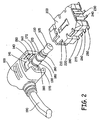
- FIG. 2 is a perspective view of an eight-pin electrical connector and jack according to an embodiment of the present invention.
- an improved eight-pin electrical connector 100 is adapted for mating with a jack 200.
- the eight-pin electrical connector 100 includes a cord 190 disposed along an upper surface of the eight-pin electrical connector 100.
- the cord 190 may be placed along other surfaces or sides of the eight-pin electrical connector 100 as desired.
- Protruding from a front side of the eight-pin electrical connector 100 is a four-pin stereo plug 105. Description of the connector 100 for use in audio connections is by way of example only and is not limiting of the types of connections for which the connector 100 may be used.
- the connector 100 of the present invention may be used as a vehicle for a variety of connection pins to corresponding contacts of a mating jack.
- the connector 100 may be used to transfer data to and from an electronic device via a connection between the connector and a mating jack such as the jack 200 described below.
- the four-pin stereo plug 105 may include a microphone contact 110, a right speaker contact 120, a left speaker contact 130, and an analog ground contact 140. Disposed between the contacts 110, 120, 130 and 140 are a plurality of insulators 180. As set forth above the contacts 110, 120, 130 and 140 may be used for a variety of other types of electrical and data connectivity.
- the four-pin stereo plug 105 are an upper pin housing 170 and a lower pin housing 172, respectively.
- the lower pin housing 172 includes a pair of additional electrical pins, for example, a data pin 150 and a power pin 160.
- the upper pin housing 170 includes additional electrical pins, for example, a clock pin 192 and a digital ground pin 196.
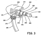
- a jack 200 according to an embodiment of the present invention is illustrated in Figures 2, 4 and 5.
- the jack 200 includes a number of contacts for establishing electrical connectivity with the pins of the eight-pin electrical connector 100.
- the contacts of the jack may be used for a variety of electrical or data connections with the connector 100.
- a pendant bus clock contact 210 and a pendant bus ground contact 220 are disposed along an outer surface of the forward end of the jack 200 for electrically mating with the contacts 192 and 196 of the eight-pin electrical connector 100.
- Additional contacts may include a microphone input contact 230, a speaker pass-through contact 240, a right speaker contact 250, a pendant bus clock contact 260, an analog ground for audio signals contact 270, and a pendant bus ground contact 280.
- Figure 4 is a perspective pictorial view of a jack according to an embodiment of the present invention.
- a number of other contacts are disposed along the other side of the jack 200 and may include, for example, a pendant bus power contact 215 and a pendant bus ground contact 220 for electrically connecting to the pins 150 and 160 of the connector 100, illustrated in Figure 2.
- Additional contacts of the jack 200 may include a pendant bus power contact 265, a left speaker contact 275, a pendant bus open collector data contact 285, and a microphone pass-through contact 295.
- Electrical connectivity between the pins of the eight-pin electrical connector 100 and the contact of the jack 200, and operation thereof, is well known to those skilled in the art.
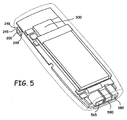
- FIG. 5 is a perspective pictorial view of a personal digital assistant showing an exterior case of the personal digital assistant in phantom and illustrating a jack 200 of the present invention integrated with the personal digital assistant 300.
- the jack 200 is integrated with the personal digital assistant (PDA) 300 such that the front face 245 of the jack 200 is flush with the outer surface of the casing (shown in phantom) of the PDA 300.
- An upper housing receiving port is adapted into the casing of the PDA 300 directly above the upper edge 248.
- a lower housing receiving port is adapted directly below the lower edge 249 of the jack 200.
- the receiving ports allow for insertion of the upper and lower pin housings 170, 172 of the eight-pin electrical connector 100, illustrated below with reference to Figure 6.
- the eight-pin electrical connector 100 is adapted for mating with the jack 200 so that the four-pin plug 105 is inserted into the entry port 235 of the jack 200 until the front surface 141 of the main connector housing comes into snug contact with the front face 245 of the jack 200.
- the upper contact housing 170 slides over the upper edge 248 of the forward section 247 of the jack 200.
- the lower contact housing 172 slides over the lower edge 249 of the forward section 247 of the jack 200.
- the pins 192 and 196 of the upper contact housing 170 engage the electrical contacts 210 and 220 of the jack 200
- the pins 150 and 160 of the lower contact housing 172 of the eight-pin electrical connector 100 engage the contacts 215 and 225 of the lower edge 249 of the forward section 247 of the jack 200.
- the upper and lower contact housings 170, 172 are inserted into the receiving ports integrated within the casing of the PDA 300 in order for the pins 150, 160, 192, 196 to engage the corresponding contacts of the jack 200.
- insertion of the upper and lower pin housings 170, 172 into the casing of the PDA 300 in order to achieve electrical contact between all pins of the eight-pin electrical connector 100 with corresponding contacts of the jack 200 creates a secure fit between the eight-pin electrical connector 100 and the jack 200 and corresponding electronic device (for example, the PDA 300) in which the jack 200 is integrated.
- FIG. 6 shows a cutaway section of the PDA 300 for illustration of the insertion of the four-pin plug 105 and the upper and lower pin housings 170 and 172 into the PDA 300 (jack 200 not illustrated in Figure 6).
- the upper and lower pin housings 170 are inserted into the interior of the PDA 300 so that the eight-pin electrical connector 100 achieves a secure connection with the jack 200 integrated interior of the PDA 300.
- stresses placed on the eight-pin electrical connector 100 from contact with foreign objects or from the mass of the eight-pin electrical connector 100 and cord 190 relative to the PDA 300 place very little stress on the electrical connections between the pins of the eight-pin electrical connector 100 and the contacts of the jack 200.
- Insertion of the upper and lower pin housings 170 and 172 into the casing of the PDA 300 insures that vibration and stresses acting on the connection between the eight-pin electrical connector 100 and the jack 200 are not directed to the electrical contacts, but instead are directed to the housing of the eight-pin electrical connector 100 and the casing of the PDA 300 which are stronger and less likely to be damaged by the introduction of stresses applied to those components.
- the cord 190 is disposed along the upper surface of the eight-pin electrical connector 100. This orientation is advantageous if the electronic device 300 is a personal digital assistant, wireless telephone, or other audio output device that may be carried in a shirt pocket or connected to a belt or other location, where an upward orientation of the cord 190 reduces additional strain on the connection between the eight-pin electrical connector 100 and the jack 200 integrated into the device 300.
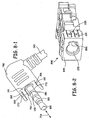
- Figures 7-1 and 7-2 are perspective illustrations of connector 100 and jack 200 which show alignment features which ensure that connector 100 can only be mated with jack 200 in a correct orientation.
- alignment or key features 702 and 704 extend from upper pin housing 170 in a direction which is generally toward lower pin housing 172.
- alignment features 702 and 704 In order to insert four-pin stereo plug 105 into entry port 235 of jack 200 far enough for the pins on the upper and lower pin housings to engage electrical contacts on jack 200 as described above, alignment features 702 and 704 must be matched with alignment grooves 706 and 708 formed in forward section 247 of the jack. This prevents the pins on connector 100 from engaging the wrong contacts on jack 200, thereby preventing potential damage to electrical components.
- FIGS 8-1, 8-2 and 9 are perspective illustrations of a connector 750 and a jack 800 in accordance with an alternate embodiment of the present invention.
- connector 750 and jack 800 have the same features as described above with reference to connector 100 and jack 200.
- Connector 750 includes an upper pin housing 770 and a lower pin housing 772.
- upper pin housing 770 of connector 750 supports pins 192 and 196.
- lower pin housing 772 of connector 750 supports pins 150 and 160.
- both of upper pin housing 770 and lower pin housing 772 includes the alignment features (i.e. alignment features 702 and 704 shown in Figure 7-1) for ensuring that connector 750 engages jack 800 with the correct orientation. Instead, an alignment feature or key 752 protrudes from front surface 141 of the main connector housing.
- alignment feature 752 protrudes from the front surface of the main connector housing adjacent to stereo plug 105. As such, alignment feature 752 extends from front surface 141 in a direction away from the front surface which is substantially parallel to a longitudinal axis 754 along which stereo plug 105 protrudes. In some embodiments, alignment feature 752 is positioned between stereo plug 105 and electrical contact pins 150 and 160, or between stereo plug 105 and electrical contact pins 192 and 196. In other words, this alignment feature also extends away from the stereo plug along a longitudinal direction of the front surface 141 of the main connector housing.
- the connector can be made considerably narrower than prior art eight-pin connectors. Further, it is has been found that the design of connector 750 allows it to be approximately 30% narrower than the design of even connector 100 of the present invention.
- Alignment feature or key 752 can be made of a number of different materials, in addition to being moved to different positions along front surface 141 between upper pin housing 770 and lower pin housing 772.
- alignment feature or key 752 can be a metal alignment feature.
- alignment feature or key 752 can be formed integrally with one of the electrical contacts of plug 105.
- alignment feature or key 752 could be formed integrally with analog ground contact 140 if desired.
- alignment feature 752 is formed from an insulating material such as plastic. In these embodiments, if desired, alignment feature 752 can be formed integrally with the insulator 180 formed closest to front surface 141.
- jack 800 in accordance with these alternate embodiments of the present invention includes a front face 845 in which entry port 235 is formed.
- front face 845 also includes an alignment groove formed contiguously with entry port 235.
- jack 800 while jack 200 would have a width of approximately 5.7 mm, jack 800 would require a width of only 4 mm. This allows connector 750 and jack 800 to be used with slimmer electronic products such as flip phones. In addition to allowing connector 750 and jack 800 to be thinner relative to connector 100 and jack 200 and relative to prior art eight-pin connectors and jacks, the alignment feature configuration on connector 750 and jack 800 provides more robust anti-rotation function.
- FIG. 10 shows a cut-away section of a PDA (or other electronic device) 900 for illustration of the insertion of the four-pin plug 105 and the upper and lower pin housings 770 and 772 into the PDA 900 (jack 800 not illustrated in Figure 10).
- the upper and lower pin housing 770 and 772 are inserted into the interior of the PDA 900 so that the eight-pin electrical connector 750 achieves a secure connection with the jack 800 integrated interior of the PDA 900.
- Alignment feature 752 both ensures that connector 750 is inserted with the correct orientation of the upper and lower pin housings, and helps to prevent rotation of connector 750 relative to PDA 900. This in turn helps to prevent damage to the pins of connector 750 and the contacts of jack 800.
- FIG 11 is a side view illustration of PDA 300 including jack 200, and of PDA 900 including jack 800.
- jack 800 including alignment groove 850 has a width (represented by arrow 902) which is significantly less than the corresponding width (represented by arrow 904) of jack 200 which includes alignment grooves 706 and 708. Again, this provides opportunity for jack 800 to be used on even thinner electronic devices than would be possible with prior art eight-pin electrical connectors and jacks.
- FIG 12 is a pictorial perspective view of a mini-USB connector plug and a mini-USB connector jack according to an embodiment of the present invention.
- the USB connector plug 500 illustrated in Figure 12 includes a printed circuit board 510 connected to a plug main body 505. Along a front surface of the plug main body 505 is a mini-USB connector plug 530 for passing data to and from an electronic device, such as a personal digital assistant 300.
- Adjacent to the USB connector plug 500 is an alignment post 525.
- Disposed on an upper surface of the alignment guide 525 is a locking latch 540.
- An alignment post guide 550 is defined along an inner side of the alignment post 525 for guiding the alignment post 525 into an alignment post port 565.
- On each side of the alignment post 525 is an electrical power contact 530.
- the USB jack 555 includes a USB connector plug port 565 for receipt of the USB connector plug 520 and an alignment post port 590 for receipt of the alignment post 525.
- a pair of electrical contacts 595 and 596 are defined along each side of the alignment post port 590 for engagement with the power contacts 530 defined along each side of the alignment post 525.
- Interior of the alignment post port 590 is a locking latch detent for engagement with the locking latch 540 when the USB connector plug 500 is connected to the USB jack 555.
- a separate power jack 575 with a power jack port 580 is disposed adjacent to the alignment post port 590 for connection of a separate electrical power contact to an electronic device in which the USB jack assembly 555 is integrated.
- the alignment post 525 has a greater length than the USB connector plug 520 so that the alignment post 525 engages the alignment post port 590 before the USB connector plug 520 engages the USB connector plug port 565.
- This configuration allows the alignment post 525 to place the plug assembly 505 in a proper orientation before introduction of the connector plug 520 into the connector plug port 565.
- small connector plugs, such as the mini-USB connector plug 520 are fragile and can become damaged if proper alignment of the connector plug to the connector plug port is not maintained during connection of the plug to the corresponding port.
- USB connector 505 of the present invention allows for the transfer of data via the connector plug, in addition to the transfer of electrical power, utilizing one connector assembly 505, as illustrated in Figure 12.
- the need to connect a separate power cord and plug to the power jack 575 is eliminated.
- use of the alignment post 525 and locking latch 540 insures a secure connection between the connector plug and the corresponding jack.
Claims (16)
- Ein verbesserter elektrischer Stecker (750), umfassend:ein Hauptsteckergehäuse;ein Stereostecker (105), der von einer vorderen Oberfläche (141) des Hauptsteckergehäuses hervorragt;ein erstes Paar elektrischer Kontakt-Pins (150, 160), das durch das Hauptsteckergehäuse auf einer ersten Seite von dem Stereostecker getragen wird;ein zweites Paar elektrischer Kontakt-Pins (192, 196), das durch das Hauptsteckergehäuse auf einer zweiten Seite von dem Stereostecker, gegenüber der ersten Seite von dem Stereostecker, getragen wird;gekennzeichnet durch
eine Ausrichtungspassform (752), die zwischen dem Stereostecker und einem von dem ersten und zweiten Paar elektrischer Kontakt-Pins positioniert ist. - Der elektrische Stecker nach Anspruch 1, wobei die Ausrichtungspassform von der vorderen Oberfläche des Hauptsteckergehäuses hervorragt.
- Der elektrische Stecker nach Anspruch 2, wobei die Ausrichtungspassform von der vorderen Oberfläche des Hauptsteckergehäuses neben dem Stereostecker hervorragt.
- Der elektrische Stecker nach Anspruch 3, wobei die Ausrichtungspassform sich von der vorderen Oberfläche in eine Richtung weg von der vorderen Oberfläche erstreckt, welche im Wesentlichen parallel zu einer Längsachse (754) ist, entlang der der Stereostecker hervorragt.
- Der elektrische Stecker nach Anspruch 4, wobei die Ausrichtungspassform sich entlang einer Längsrichtung der vorderen Oberfläche des Hauptsteckergehäuses von dem Stereostecker weg erstreckt.
- Der elektrische Stecker nach Anspruch 5, wobei der Stereostecker umfasst:eine Vielzahl von elektrischen Kontakten (110, 120, 130, 140), die entlang der Längsachse des Stereosteckers in Abständen getrennt angeordnet sind; undeine Vielzahl von Isolatoren (180), die entlang der Längsachse des Stereosteckers in Abständen getrennt angeordnet sind, wobei jeder der Vielzahl von Isolatoren benachbarte der Vielzahl von elektrischen Kontakten elektrisch trennt.
- Der elektrische Stecker nach Anspruch 6, wobei die Ausrichtungspassform mit einem der Vielzahl von elektrischen Isolatoren des Stereosteckers integriert gebildet ist.
- Der elektrische Stecker nach Anspruch 6, wobei die Ausrichtungspassform mit einem der Vielzahl von elektrischen Kontakten des Stereosteckers integriert gebildet ist.
- Der elektrische Stecker nach Anspruch 2, wobei das Hauptsteckergehäuse des Weiteren umfasst:ein oberes Pin-Gehäuse (770), wobei das obere Pin-Gehäuse eine äußere Oberfläche und eine innere Oberfläche aufweist, wobei die äußere Oberfläche eine kontinuierliche Oberfläche mit einer Oberfläche des Hauptsteckergehäuses bildet, und wobei das erste Paar elektrischer Kontakt-Pins entlang der inneren Oberfläche des oberen Gehäuses angeordnet ist;ein unteres Pin-Gehäuse (772), das in einer räumlich getrennten Beziehung zu dem oberen Pin-Gehäuse angeordnet ist, wobei das untere Pin-Gehäuse eine äußere Oberfläche und eine innere Oberfläche aufweist, wobei die äußere Oberfläche eine kontinuierliche Oberfläche mit der Oberfläche des Hauptsteckergehäuses bildet, wobei die innere Oberfläche gegenüber der inneren Oberfläche des oberen Pin-Gehäuses liegt, und wobei das zweite Paar elektrischer Kontakt-Pins entlang der inneren Oberfläche des unteren Pin-Gehäuses angeordnet ist; undwobei der Stereostecker von der vorderen Oberfläche des Hauptsteckergehäuses zwischen der inneren Oberfläche des unteren Pin-Gehäuses und der inneren Oberfläche des oberen Pin-Gehäuses hervorragt.
- Der elektrische Stecker nach Anspruch 9, wobei der elektrische Stecker angepasst ist, sich mit einer Buchse (800) zu verbinden, wobei der Stereostecker angepasst ist, verbindend in einen Steckeranschluss (235) der Buchse eingeführt zu werden, und wobei das obere Pin-Gehäuse und das untere Pin-Gehäuse so angepasst sind, dass sie verbindend mit dem vorderen Steckeranschlussgehäuse der Buchse in Eingriff stehen.
- Der elektrische Stecker nach Anspruch 10, wobei der Stereostecker eine Vielzahl von elektrischen Kontakt-Pins (110, 120, 130, 140) einschließt, die mit einer entsprechende Vielzahl von elektrischen Kontakten, die entlang einer inneren Oberfläche des Steckeranschlusses der Buchse angeordnet sind, in Eingriff stehen.
- Der elektrische Stecker nach Anspruch 11, wobei die Vielzahl elektrischer Kontakt-Pins des Stereosteckers umfasst:einen Mikrofonkontakt;einen rechten Lautsprecherkontakt;einen linken Lautsprecherkontakt; undeinen analogen Massekontakt.
- Der elektrische Stecker nach Anspruch 11, wobei ein erstes Paar elektrischer Kontakt-Pins mit einem entsprechenden Paar elektrischer Kontakte (215, 225), die entlang einer oberen Oberfläche eines vorderen Abschnitts des Steckeranschlussgehäuses der Buchse angeordnet sind, in Eingriff steht.
- Der elektrische Stecker nach Anspruch 13, wobei das zweite Paar elektrischer Kontakt-Pins mit einem entsprechenden Paar elektrischer Kontakte, die entlang einer unteren Oberfläche eines vorderen Abschnitts des Steckeranschlussgehäuses der Buchse angeordnet sind, in Eingriff steht.
- Der elektrische Kontakt nach Anspruch 14,
wobei die Buchse in einem Gehäuse eines elektronischen Gerätes (900) angebracht ist, so dass eine Stirnfläche des vorderen Abschnitts der Buchse bündig mit einer äußeren Oberfläche des Gehäuses des elektronischen Gerätes ist;
wobei ein Anschluss, der ein oberes Gehäuse aufnimmt, in dem Gehäuse direkt oberhalb der oberen Oberfläche des vorderen Abschnitts der Buchse definiert ist;
wobei ein Anschluss, der ein unteres Gehäuse aufnimmt, in dem Gehäuse direkt unterhalb der unteren Oberfläche des vorderen Abschnitts der Buchse definiert ist; und
wobei das obere Pin-Gehäuse, wenn der elektrische Stecker mit der Buchse verbunden wird, in den Anschluss, der ein oberes Gehäuse aufnimmt, eingeführt wird und das untere Pin-Gehäuse in den Anschluss, der ein unteres Gehäuse aufnimmt, eingeführt wird, so dass der elektrische Stecker mit dem Gehäuse des elektronischen Gerätes zusammenpasst. - Ein elektronisches Gerät, das die Buchse nach Anspruch 13 einschließt, wobei der elektrische Stecker so angepasst ist, dass er sich mit der Buchse verbindet.
Applications Claiming Priority (2)
| Application Number | Priority Date | Filing Date | Title |
|---|---|---|---|
| US648182 | 2003-08-26 | ||
| US10/648,182 US6964586B2 (en) | 2002-02-08 | 2003-08-26 | Reduced size eight-pin audio jack electrical connector |
Publications (2)
| Publication Number | Publication Date |
|---|---|
| EP1511128A1 EP1511128A1 (de) | 2005-03-02 |
| EP1511128B1 true EP1511128B1 (de) | 2007-06-06 |
Family
ID=34104663
Family Applications (1)
| Application Number | Title | Priority Date | Filing Date |
|---|---|---|---|
| EP04019430A Not-in-force EP1511128B1 (de) | 2003-08-26 | 2004-08-16 | Achtpoliger-Audio-Steckbuchse-Verbinder mit reduzierten Abmessungen |
Country Status (7)
| Country | Link |
|---|---|
| US (1) | US6964586B2 (de) |
| EP (1) | EP1511128B1 (de) |
| JP (1) | JP2005072005A (de) |
| KR (1) | KR100937274B1 (de) |
| CN (1) | CN100481645C (de) |
| AT (1) | ATE364244T1 (de) |
| DE (1) | DE602004006809T2 (de) |
Families Citing this family (33)
| Publication number | Priority date | Publication date | Assignee | Title |
|---|---|---|---|---|
| BR0108844A (pt) * | 2000-02-29 | 2002-12-03 | Kyocera Corp | Terminal de informações portátil e câmara digital para terminal de informações portátil e sistema de câmara digital/terminal de informações portátil |
| WO2006027640A1 (en) * | 2004-09-10 | 2006-03-16 | Nokia Corporation | Audio and video plug and socket having integrated video contact |
| TWM278139U (en) * | 2005-06-07 | 2005-10-11 | He And Technology Co Ltd | Small USB connector |
| US7238059B1 (en) * | 2006-06-06 | 2007-07-03 | Cheng Uei Precision Industry Co., Ltd. | Audio jack connector |
| JP5151100B2 (ja) * | 2006-09-08 | 2013-02-27 | ソニー株式会社 | プラグ、音声入出力装置及びノイズキャンセルシステム |
| JP2008066175A (ja) * | 2006-09-08 | 2008-03-21 | Sony Corp | プラグ |
| US8090130B2 (en) * | 2006-09-11 | 2012-01-03 | Apple Inc. | Highly portable media devices |
| US7407416B1 (en) * | 2006-09-27 | 2008-08-05 | Sprint Communications Company L.P. | Multi-stage multi-pole connector |
| CN101207256B (zh) * | 2006-12-20 | 2010-09-29 | 鸿富锦精密工业(深圳)有限公司 | 一种音频信号转接装置 |
| US7741556B2 (en) * | 2007-01-10 | 2010-06-22 | Zero Crossing Inc | Methods and systems for interfacing an electric stringed musical instrument to an electronic device |
| US7591673B2 (en) * | 2007-01-18 | 2009-09-22 | Hewlett-Packard Development Company, L.P. | Combined power and control signal cable |
| US7749028B2 (en) | 2007-10-19 | 2010-07-06 | Sony Ericsson Mobile Communications Ab | Micro USB compatible combo system connector |
| US7537489B2 (en) * | 2007-10-19 | 2009-05-26 | Sony Ericsson Mobile Communications Ab | Micro USB compatible combo system controller |
| TWI419431B (zh) * | 2008-11-06 | 2013-12-11 | 財團法人工業技術研究院 | 電能管理插座架構 |
| US7927151B2 (en) * | 2009-06-05 | 2011-04-19 | Apple Inc. | Audio plug with core structural member |
| US7824229B1 (en) * | 2009-07-10 | 2010-11-02 | Cheng Uei Precision Industry Co., Ltd. | Audio plug connector |
| US7824228B1 (en) * | 2009-08-18 | 2010-11-02 | Cheng Uei Precision Industry Co., Ltd. | Audio plug connector |
| CN102377056B (zh) * | 2010-08-12 | 2014-01-22 | 鸿富锦精密工业(深圳)有限公司 | 音频连接器及其音频插头 |
| US8864514B2 (en) * | 2010-10-07 | 2014-10-21 | General Electric Company | Controller device |
| GB2489424B (en) * | 2011-03-25 | 2015-12-30 | Ifpl Group Ltd | Electrical connectors |
| US8632354B2 (en) | 2011-08-16 | 2014-01-21 | Micron Technology, Inc. | Interconnection systems |
| US9239633B1 (en) | 2012-09-07 | 2016-01-19 | Google Inc. | System and method for device having internal reset/restart button that is activated via insertion tool accessiable throught single transmission path of plug connection |
| USD733685S1 (en) * | 2013-01-04 | 2015-07-07 | First Act, Inc. | Audio adapter |
| US9093798B2 (en) * | 2013-01-04 | 2015-07-28 | Lenovo (Singapore) Pte. Ltd. | Combination power and data connector |
| US9176537B2 (en) | 2013-03-15 | 2015-11-03 | Intel Corporation | Connector assembly for an electronic device |
| CN103887643B (zh) * | 2014-03-17 | 2016-04-13 | 小米科技有限责任公司 | 耳机插座、电子器件、电子设备及电子系统 |
| CN106356687A (zh) * | 2016-09-26 | 2017-01-25 | 南京金龙客车制造有限公司 | 一种柔性太阳能电池板用接线插件 |
| US10312611B2 (en) | 2017-03-30 | 2019-06-04 | Microsoft Technology Licensing, Llc | Connector for use with printed circuit board |
| CN107204554A (zh) * | 2017-06-12 | 2017-09-26 | 中国汽车技术研究中心 | 一种车用多功能插头 |
| CN107394478A (zh) * | 2017-07-31 | 2017-11-24 | 环胜电子(深圳)有限公司 | 连接器组合 |
| CN108736256A (zh) * | 2018-07-11 | 2018-11-02 | 嘉兴市金利达电子有限公司 | 一种防脱落的音频线接头 |
| USD975645S1 (en) * | 2018-12-04 | 2023-01-17 | Klein Electronics, Inc. | Secure audio accessory connector |
| CN113097789B (zh) * | 2019-12-20 | 2023-07-18 | 明基智能科技(上海)有限公司 | 无线传输装置 |
Family Cites Families (12)
| Publication number | Priority date | Publication date | Assignee | Title |
|---|---|---|---|---|
| US4897055A (en) | 1988-11-28 | 1990-01-30 | International Business Machines Corp. | Sequential Connecting device |
| US4972491A (en) * | 1988-11-30 | 1990-11-20 | Wilcox Jr Edward R | Ear-mic headset/eardefender |
| US5118309A (en) * | 1991-04-01 | 1992-06-02 | Motorola, Inc. | Minimum wire interface for multiple accessories |
| US5530375A (en) | 1992-12-24 | 1996-06-25 | International Business Machines Corporation | Method of testing circuits and/or burning-in chips |
| JP3261448B2 (ja) | 1997-06-02 | 2002-03-04 | エスエムケイ株式会社 | 多極コネクター |
| JP4355376B2 (ja) * | 1998-03-27 | 2009-10-28 | ソニー株式会社 | オーディオおよびデータ通信用ジャック、再生装置 |
| KR200252401Y1 (ko) * | 1998-09-26 | 2001-12-28 | 윤종용 | 커넥터어셈블리 |
| CH690393A5 (fr) * | 1999-06-28 | 2000-08-15 | Armand D Touboul | Tête de connexion pour casque d'écoute stéréophonique. |
| TW438168U (en) * | 1999-10-06 | 2001-05-28 | Liau Sheng Shing | Assembled structure of reeling box with replaceable switching socket |
| US6250967B1 (en) | 2000-02-11 | 2001-06-26 | Fa-Yu Chu | Mobile video device |
| CA2360818A1 (en) * | 2001-10-31 | 2003-04-30 | Jui-Shu Huang | Multichannel phone plug |
| US6626706B2 (en) | 2002-02-08 | 2003-09-30 | Microsoft Corporation | Eight-pin electrical connector and USB connector |
-
2003
- 2003-08-26 US US10/648,182 patent/US6964586B2/en not_active Expired - Fee Related
-
2004
- 2004-08-16 AT AT04019430T patent/ATE364244T1/de not_active IP Right Cessation
- 2004-08-16 DE DE602004006809T patent/DE602004006809T2/de active Active
- 2004-08-16 EP EP04019430A patent/EP1511128B1/de not_active Not-in-force
- 2004-08-23 JP JP2004242810A patent/JP2005072005A/ja active Pending
- 2004-08-25 KR KR1020040067232A patent/KR100937274B1/ko not_active IP Right Cessation
- 2004-08-26 CN CNB2004100685467A patent/CN100481645C/zh not_active Expired - Fee Related
Non-Patent Citations (1)
| Title |
|---|
| None * |
Also Published As
| Publication number | Publication date |
|---|---|
| JP2005072005A (ja) | 2005-03-17 |
| CN1606199A (zh) | 2005-04-13 |
| KR20050021282A (ko) | 2005-03-07 |
| EP1511128A1 (de) | 2005-03-02 |
| ATE364244T1 (de) | 2007-06-15 |
| KR100937274B1 (ko) | 2010-01-18 |
| US6964586B2 (en) | 2005-11-15 |
| DE602004006809D1 (de) | 2007-07-19 |
| US20040038593A1 (en) | 2004-02-26 |
| DE602004006809T2 (de) | 2007-10-11 |
| CN100481645C (zh) | 2009-04-22 |
Similar Documents
| Publication | Publication Date | Title |
|---|---|---|
| EP1511128B1 (de) | Achtpoliger-Audio-Steckbuchse-Verbinder mit reduzierten Abmessungen | |
| US6626706B2 (en) | Eight-pin electrical connector and USB connector | |
| US11217942B2 (en) | Connector having metal shell with anti-displacement structure | |
| EP0892468B1 (de) | Elektrische Verbinderanordnung mit Polarisationsmittel | |
| US7059892B1 (en) | Electrical connector and backshell | |
| US7128617B2 (en) | Electrical socket assembly and plug connector coupled thereto | |
| US6575793B1 (en) | Audio jack connector | |
| US7520760B2 (en) | Electrical connector having blade terminals | |
| US5240436A (en) | BNC-RJ conversion connector | |
| US20080057791A1 (en) | Jack connector | |
| US6503101B1 (en) | Electrical connector having grounding path | |
| JP2005531119A (ja) | 電線処理モジュールを備えた電気コネクタ | |
| US7445515B1 (en) | Audio jack | |
| EP1166400B1 (de) | Elektrischer verbinder | |
| US6099332A (en) | Connector with adaptable insert | |
| EP1276181B1 (de) | Elektrischer Verbinder zum Aufnahme eines Steckers | |
| US6354870B1 (en) | Apparatus and method for mounting small electrical connector | |
| US7402054B2 (en) | Board-to-board connector | |
| US6224409B1 (en) | Audio jack | |
| US6461200B1 (en) | Electrical connector assembly | |
| US6676423B1 (en) | Modular electrical connector assembly providing electrostatic discharge upon insertion of a mating connector | |
| US20030119342A1 (en) | Rotatably mated connector couple | |
| WO2011140988A1 (zh) | 电连接器插头 | |
| WO2002089264A3 (en) | Electrical connector for connecting flat flexible cricuitry to discrete terminal pins | |
| US6793538B2 (en) | Slim modular jack |
Legal Events
| Date | Code | Title | Description |
|---|---|---|---|
| PUAI | Public reference made under article 153(3) epc to a published international application that has entered the european phase |
Free format text: ORIGINAL CODE: 0009012 |
|
| AK | Designated contracting states |
Kind code of ref document: A1 Designated state(s): AT BE BG CH CY CZ DE DK EE ES FI FR GB GR HU IE IT LI LU MC NL PL PT RO SE SI SK TR |
|
| AX | Request for extension of the european patent |
Extension state: AL HR LT LV MK |
|
| 17P | Request for examination filed |
Effective date: 20050726 |
|
| AKX | Designation fees paid |
Designated state(s): AT BE BG CH CY CZ DE DK EE ES FI FR GB GR HU IE IT LI LU MC NL PL PT RO SE SI SK TR |
|
| GRAP | Despatch of communication of intention to grant a patent |
Free format text: ORIGINAL CODE: EPIDOSNIGR1 |
|
| GRAS | Grant fee paid |
Free format text: ORIGINAL CODE: EPIDOSNIGR3 |
|
| GRAA | (expected) grant |
Free format text: ORIGINAL CODE: 0009210 |
|
| AK | Designated contracting states |
Kind code of ref document: B1 Designated state(s): AT BE BG CH CY CZ DE DK EE ES FI FR GB GR HU IE IT LI LU MC NL PL PT RO SE SI SK TR |
|
| PG25 | Lapsed in a contracting state [announced via postgrant information from national office to epo] |
Ref country code: LI Free format text: LAPSE BECAUSE OF FAILURE TO SUBMIT A TRANSLATION OF THE DESCRIPTION OR TO PAY THE FEE WITHIN THE PRESCRIBED TIME-LIMIT Effective date: 20070606 Ref country code: CH Free format text: LAPSE BECAUSE OF FAILURE TO SUBMIT A TRANSLATION OF THE DESCRIPTION OR TO PAY THE FEE WITHIN THE PRESCRIBED TIME-LIMIT Effective date: 20070606 Ref country code: FI Free format text: LAPSE BECAUSE OF FAILURE TO SUBMIT A TRANSLATION OF THE DESCRIPTION OR TO PAY THE FEE WITHIN THE PRESCRIBED TIME-LIMIT Effective date: 20070606 |
|
| REG | Reference to a national code |
Ref country code: GB Ref legal event code: FG4D |
|
| REG | Reference to a national code |
Ref country code: CH Ref legal event code: EP |
|
| REG | Reference to a national code |
Ref country code: IE Ref legal event code: FG4D |
|
| REF | Corresponds to: |
Ref document number: 602004006809 Country of ref document: DE Date of ref document: 20070719 Kind code of ref document: P |
|
| PG25 | Lapsed in a contracting state [announced via postgrant information from national office to epo] |
Ref country code: SE Free format text: LAPSE BECAUSE OF FAILURE TO SUBMIT A TRANSLATION OF THE DESCRIPTION OR TO PAY THE FEE WITHIN THE PRESCRIBED TIME-LIMIT Effective date: 20070906 |
|
| PG25 | Lapsed in a contracting state [announced via postgrant information from national office to epo] |
Ref country code: ES Free format text: LAPSE BECAUSE OF FAILURE TO SUBMIT A TRANSLATION OF THE DESCRIPTION OR TO PAY THE FEE WITHIN THE PRESCRIBED TIME-LIMIT Effective date: 20070917 |
|
| ET | Fr: translation filed | ||
| PG25 | Lapsed in a contracting state [announced via postgrant information from national office to epo] |
Ref country code: PL Free format text: LAPSE BECAUSE OF FAILURE TO SUBMIT A TRANSLATION OF THE DESCRIPTION OR TO PAY THE FEE WITHIN THE PRESCRIBED TIME-LIMIT Effective date: 20070606 Ref country code: AT Free format text: LAPSE BECAUSE OF FAILURE TO SUBMIT A TRANSLATION OF THE DESCRIPTION OR TO PAY THE FEE WITHIN THE PRESCRIBED TIME-LIMIT Effective date: 20070606 |
|
| NLV1 | Nl: lapsed or annulled due to failure to fulfill the requirements of art. 29p and 29m of the patents act | ||
| REG | Reference to a national code |
Ref country code: CH Ref legal event code: PL |
|
| PG25 | Lapsed in a contracting state [announced via postgrant information from national office to epo] |
Ref country code: BE Free format text: LAPSE BECAUSE OF FAILURE TO SUBMIT A TRANSLATION OF THE DESCRIPTION OR TO PAY THE FEE WITHIN THE PRESCRIBED TIME-LIMIT Effective date: 20070606 |
|
| PG25 | Lapsed in a contracting state [announced via postgrant information from national office to epo] |
Ref country code: SI Free format text: LAPSE BECAUSE OF FAILURE TO SUBMIT A TRANSLATION OF THE DESCRIPTION OR TO PAY THE FEE WITHIN THE PRESCRIBED TIME-LIMIT Effective date: 20070606 Ref country code: BG Free format text: LAPSE BECAUSE OF FAILURE TO SUBMIT A TRANSLATION OF THE DESCRIPTION OR TO PAY THE FEE WITHIN THE PRESCRIBED TIME-LIMIT Effective date: 20070906 Ref country code: NL Free format text: LAPSE BECAUSE OF FAILURE TO SUBMIT A TRANSLATION OF THE DESCRIPTION OR TO PAY THE FEE WITHIN THE PRESCRIBED TIME-LIMIT Effective date: 20070606 Ref country code: CZ Free format text: LAPSE BECAUSE OF FAILURE TO SUBMIT A TRANSLATION OF THE DESCRIPTION OR TO PAY THE FEE WITHIN THE PRESCRIBED TIME-LIMIT Effective date: 20070606 Ref country code: PT Free format text: LAPSE BECAUSE OF FAILURE TO SUBMIT A TRANSLATION OF THE DESCRIPTION OR TO PAY THE FEE WITHIN THE PRESCRIBED TIME-LIMIT Effective date: 20071106 |
|
| PG25 | Lapsed in a contracting state [announced via postgrant information from national office to epo] |
Ref country code: SK Free format text: LAPSE BECAUSE OF FAILURE TO SUBMIT A TRANSLATION OF THE DESCRIPTION OR TO PAY THE FEE WITHIN THE PRESCRIBED TIME-LIMIT Effective date: 20070606 |
|
| PLBE | No opposition filed within time limit |
Free format text: ORIGINAL CODE: 0009261 |
|
| STAA | Information on the status of an ep patent application or granted ep patent |
Free format text: STATUS: NO OPPOSITION FILED WITHIN TIME LIMIT |
|
| PG25 | Lapsed in a contracting state [announced via postgrant information from national office to epo] |
Ref country code: DK Free format text: LAPSE BECAUSE OF FAILURE TO SUBMIT A TRANSLATION OF THE DESCRIPTION OR TO PAY THE FEE WITHIN THE PRESCRIBED TIME-LIMIT Effective date: 20070606 Ref country code: GR Free format text: LAPSE BECAUSE OF FAILURE TO SUBMIT A TRANSLATION OF THE DESCRIPTION OR TO PAY THE FEE WITHIN THE PRESCRIBED TIME-LIMIT Effective date: 20070907 Ref country code: MC Free format text: LAPSE BECAUSE OF NON-PAYMENT OF DUE FEES Effective date: 20070831 |
|
| 26N | No opposition filed |
Effective date: 20080307 |
|
| PG25 | Lapsed in a contracting state [announced via postgrant information from national office to epo] |
Ref country code: RO Free format text: LAPSE BECAUSE OF FAILURE TO SUBMIT A TRANSLATION OF THE DESCRIPTION OR TO PAY THE FEE WITHIN THE PRESCRIBED TIME-LIMIT Effective date: 20070606 |
|
| PG25 | Lapsed in a contracting state [announced via postgrant information from national office to epo] |
Ref country code: IE Free format text: LAPSE BECAUSE OF NON-PAYMENT OF DUE FEES Effective date: 20070816 |
|
| PG25 | Lapsed in a contracting state [announced via postgrant information from national office to epo] |
Ref country code: EE Free format text: LAPSE BECAUSE OF FAILURE TO SUBMIT A TRANSLATION OF THE DESCRIPTION OR TO PAY THE FEE WITHIN THE PRESCRIBED TIME-LIMIT Effective date: 20070606 |
|
| PG25 | Lapsed in a contracting state [announced via postgrant information from national office to epo] |
Ref country code: CY Free format text: LAPSE BECAUSE OF FAILURE TO SUBMIT A TRANSLATION OF THE DESCRIPTION OR TO PAY THE FEE WITHIN THE PRESCRIBED TIME-LIMIT Effective date: 20070606 |
|
| PG25 | Lapsed in a contracting state [announced via postgrant information from national office to epo] |
Ref country code: LU Free format text: LAPSE BECAUSE OF NON-PAYMENT OF DUE FEES Effective date: 20070816 |
|
| PG25 | Lapsed in a contracting state [announced via postgrant information from national office to epo] |
Ref country code: TR Free format text: LAPSE BECAUSE OF FAILURE TO SUBMIT A TRANSLATION OF THE DESCRIPTION OR TO PAY THE FEE WITHIN THE PRESCRIBED TIME-LIMIT Effective date: 20070606 Ref country code: HU Free format text: LAPSE BECAUSE OF FAILURE TO SUBMIT A TRANSLATION OF THE DESCRIPTION OR TO PAY THE FEE WITHIN THE PRESCRIBED TIME-LIMIT Effective date: 20071207 |
|
| PGFP | Annual fee paid to national office [announced via postgrant information from national office to epo] |
Ref country code: DE Payment date: 20140901 Year of fee payment: 11 |
|
| PGFP | Annual fee paid to national office [announced via postgrant information from national office to epo] |
Ref country code: GB Payment date: 20140725 Year of fee payment: 11 Ref country code: FR Payment date: 20140725 Year of fee payment: 11 |
|
| PGFP | Annual fee paid to national office [announced via postgrant information from national office to epo] |
Ref country code: IT Payment date: 20140820 Year of fee payment: 11 |
|
| REG | Reference to a national code |
Ref country code: DE Ref legal event code: R082 Ref document number: 602004006809 Country of ref document: DE Representative=s name: GRUENECKER, KINKELDEY, STOCKMAIR & SCHWANHAEUS, DE |
|
| REG | Reference to a national code |
Ref country code: GB Ref legal event code: 732E Free format text: REGISTERED BETWEEN 20150108 AND 20150114 |
|
| REG | Reference to a national code |
Ref country code: DE Ref legal event code: R081 Ref document number: 602004006809 Country of ref document: DE Owner name: MICROSOFT TECHNOLOGY LICENSING, LLC, REDMOND, US Free format text: FORMER OWNER: MICROSOFT CORP., REDMOND, WASH., US Effective date: 20150126 Ref country code: DE Ref legal event code: R082 Ref document number: 602004006809 Country of ref document: DE Representative=s name: GRUENECKER PATENT- UND RECHTSANWAELTE PARTG MB, DE Effective date: 20150126 |
|
| REG | Reference to a national code |
Ref country code: FR Ref legal event code: TP Owner name: MICROSOFT TECHNOLOGY LICENSING, LLC, US Effective date: 20150724 |
|
| REG | Reference to a national code |
Ref country code: DE Ref legal event code: R119 Ref document number: 602004006809 Country of ref document: DE |
|
| GBPC | Gb: european patent ceased through non-payment of renewal fee |
Effective date: 20150816 |
|
| PG25 | Lapsed in a contracting state [announced via postgrant information from national office to epo] |
Ref country code: IT Free format text: LAPSE BECAUSE OF NON-PAYMENT OF DUE FEES Effective date: 20150816 |
|
| REG | Reference to a national code |
Ref country code: FR Ref legal event code: ST Effective date: 20160429 |
|
| PG25 | Lapsed in a contracting state [announced via postgrant information from national office to epo] |
Ref country code: GB Free format text: LAPSE BECAUSE OF NON-PAYMENT OF DUE FEES Effective date: 20150816 Ref country code: DE Free format text: LAPSE BECAUSE OF NON-PAYMENT OF DUE FEES Effective date: 20160301 |
|
| PG25 | Lapsed in a contracting state [announced via postgrant information from national office to epo] |
Ref country code: FR Free format text: LAPSE BECAUSE OF NON-PAYMENT OF DUE FEES Effective date: 20150831 |