US6676423B1 - Modular electrical connector assembly providing electrostatic discharge upon insertion of a mating connector - Google Patents
Modular electrical connector assembly providing electrostatic discharge upon insertion of a mating connector Download PDFInfo
- Publication number
- US6676423B1 US6676423B1 US09/560,990 US56099000A US6676423B1 US 6676423 B1 US6676423 B1 US 6676423B1 US 56099000 A US56099000 A US 56099000A US 6676423 B1 US6676423 B1 US 6676423B1
- Authority
- US
- United States
- Prior art keywords
- connector assembly
- shorting bar
- contact
- plug
- shield
- Prior art date
- Legal status (The legal status is an assumption and is not a legal conclusion. Google has not performed a legal analysis and makes no representation as to the accuracy of the status listed.)
- Expired - Fee Related
Links
Images


Classifications
-
- H—ELECTRICITY
- H01—ELECTRIC ELEMENTS
- H01R—ELECTRICALLY-CONDUCTIVE CONNECTIONS; STRUCTURAL ASSOCIATIONS OF A PLURALITY OF MUTUALLY-INSULATED ELECTRICAL CONNECTING ELEMENTS; COUPLING DEVICES; CURRENT COLLECTORS
- H01R13/00—Details of coupling devices of the kinds covered by groups H01R12/70 or H01R24/00 - H01R33/00
- H01R13/648—Protective earth or shield arrangements on coupling devices, e.g. anti-static shielding
- H01R13/6485—Electrostatic discharge protection
Definitions
- the present invention relates generally to a modular electrical connector assembly, such as a modular jack, and more specifically to a modular jack which provides electrostatic discharge upon insertion of a mating plug so that problems arising from electrostatic discharge from the plug through the jack to the substrate on which the jack is mounted are avoided.
- a data transmission device with a mating connector assembly, such as a computer
- this charge can be immediately transferred from the cord through the connector assembly and to the printed circuit board on which the connector assembly is mounted.
- this charge can damage expensive circuitry on the printed circuit board.
- an electrical connector assembly in accordance with the invention includes a jack defining a plug-receiving receptacle, at least one contact having a contact portion situated in the receptacle, the contact portion being electrically couplable to the substrate, and static charge discharge means arranged in electrical connection with the contact(s) for discharging static charge from a plug upon insertion into the receptacle and engagement with the contact(s).
- the static charge discharge means preferably include a shield surrounding at least a portion of the jack and establish a path to ground from the contact(s) to the ground region of the substrate through the shield.
- the jack may comprise a housing including an outer housing part and an inner housing part situated at least partially in the outer housing part.
- the outer housing part includes a comb portion defining a plurality of slots, each slot receiving an end portion of a respective contact.
- the outer housing part includes a channel in communication with all of the slots and possibly extending in a direction perpendicular to a longitudinal direction of the jack.
- the static charge discharge means comprises a shorting bar arranged in the channel in engagement with the end portions of the contacts received in the slots.
- the shorting bar is electrically connected to the shield, e.g., directly or, in the alternative, indirectly through a connecting pin.
- the contacts may be unitary contacts, each having, in addition to the contact portion, a terminal portion adapted to be connected to the substrate.
- FIG. 1 is a side view of a modular electrical connector assembly in accordance with the invention.
- FIG. 2 is a partially broken-away view of a modular electrical connector assembly in accordance with the invention.
- FIG. 3 is an exploded view of a modular electrical connector assembly in accordance with the invention.
- FIG. 4 is a broken-away view of a modular electrical connector assembly in accordance with the invention.
- FIG. 5 is a broken-away view of a modular electrical connector assembly in accordance with the invention being used in conjunction with a modular plug.
- FIG. 6 is a broken-away view of a modular electrical connector assembly in accordance with the invention being used in conjunction with a modular plug.
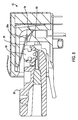
- FIG. 1 shows a side view of a modular electrical connector assembly designated 10 designed for mounting on a substrate such as a printed circuit board.
- the connector assembly 10 includes a jack 12 and a shield 14 surrounding at least a portion of the jack 12 .
- Shield 14 is formed from a metallic material and includes projections 14 a adapted to be connected to ground regions of a substrate, such as a printed circuit board, on which the connector assembly 10 is mounted.
- Jack 12 includes an outer housing part 16 and an inner housing part 18 situated in engagement with and at least partially within the outer housing part 16 to define a plug-receiving receptacle 20 (FIG. 2 ).
- the outer and inner housing parts 16 , 18 may have the same general form as existing single-port modular jacks, such as those disclosed in U.S. Pat. No. 4,703,991 (assigned to the current assignee incorporated by reference herein in its entirety). However, differing from the jacks disclosed in the '991 patent, an elongate, substantially cylindrical channel 22 is formed in the comb portion 24 of the outer housing part 16 and at least one side walls of the outer housing part 16 is formed with aperture in alignment with the channel 22 .
- the comb portion 24 also defines a plurality of substantially parallel slots 26 , each slot 26 being receivable of an end portion 28 a of the contact 28 situated in connection with at least the inner housing part 18 .
- Channel 22 is open over at least a radial portion thereof to communicate with all of the slots 26 .
- the connector assembly 10 also includes a shorting bar 30 arranged in the channel 22 . As shown in FIG. 2, the end portion 28 a of the contacts 28 engages the shorting bar 30 in view of the construction of the contacts 28 to be biased against the lower surface of the slots 26 .
- the comb portion 24 and channel 22 could be designed such that the end portions 28 a of the contacts 28 contact both the shorting bar 30 and the lower surface of the slots 26 .
- the shorting bar 30 is constructed to extend through a side wall of the jack 12 to be connected to the shield 14 and thereby establish an electrical connection between the shorting bar 30 and the shield 14 .
- the channel 22 and thus the shorting bar 30 could be designed to extend over only the slots 26 and a separate connector pin or any other electrically transmitting member provided to electrically connect the shorting bar 30 to the shield 14 .
- shield 14 is electrically connected to ground on the printed circuit board on which the connector assembly 10 is mounted.
- the shorting bar 30 is connected to ground through the shield 14 of the connector assembly 10 .
- the jack 12 also includes terminal portions 32 adapted for connection to the substrate on which the connector assembly 10 is mounted and which may be part of contacts 28 or separate.
- the end portions 28 a of the contacts 28 engage the shorting bar 30 (as shown in FIG. 2 ).
- any static charge built up on the cable to which the plug is connected is carried away as such charge is transmitted through contacts 28 to the shorting bar 30 and from the shorting bar 30 to the shield 14 and from the shield 14 to the ground on the printed circuit board on which the connector assembly 10 is mounted. This is because the contacts 28 are all in contact with shorting bar 30 when the connector assembly 10 is in an unmated state.
- the end portions 28 a of contacts 28 are urged out of contact with the shorting bar 30 and the shorting bar 30 does not affect data transmission between the plug and connector assembly 10 . Accordingly, using the connector assembly 10 in accordance with the invention, the static charge on the cable to which the plug is attached is discharged and eliminated and is therefore not transmitted to the circuitry on the printed circuit board on which the connector assembly is mounted.
- FIG. 3 shows an exploded view of an electrical connector assembly 10 including jack 12 and shield 14 surrounding at least a portion of jack 12 .
- Shield 14 is formed from a metallic material and includes projections 14 a adapted to be connected to ground regions of a substrate, such as a printed circuit board, on which the connector assembly 10 is mounted.
- Jack 12 includes an outer housing part 16 , an inner housing part 18 situated in engagement with and at least partially within the outer housing part 16 , to define a plug-receiving receptacle 20 . It also includes a shorting bar 50 situated within plug-receiving receptacle 20 , between inner housing part 18 and outer housing part 16 .
- Shorting bar 50 includes grounding projection 52 and spring-like fingers 54 .
- Grounding projection 52 is adapted to be connected to ground regions of a substrate, such as a printed circuit board, on which the connector assembly 10 is mounted. Alternately, grounding projection 52 can be configured to electrically engage shield 14 and ground through projections 14 a which are adapted to be connected to ground regions of a substrate.
- the outer and inner housing parts 16 , 18 may have the same general form as existing single-port modular jacks, such as those disclosed in U.S. Pat. No. 4,703,991 (assigned to the current assignee incorporated by reference herein in its entirety). However, differing from the jacks disclosed in the '991 patent, is the inclusion of the shorting bar 50 in between inner housing part 18 and outer housing part 16 .
- the comb portion 24 also defines a plurality of substantially parallel slots 26 , each slot 26 being receivable of a finger 54 of the shorting bar 50 . As shown in FIG. 4, the end portions 28 a of the contacts 28 engage the fingers 54 in view of the construction of the contacts 28 to be biased towards the lower surface of the slots 26 .
- the jack 12 also includes terminal portions 32 adapted for connection to the substrate on which the connector assembly 10 is mounted and which may be part of contacts 28 or separate.
- any static charge built up in the cable to which the plug is connected is carried away as such charge is transmitted from terminals 62 through the contacts 28 to the shorting bar 50 , via fingers 54 , and from shorting bar 50 to the ground, via grounding projection 52 , on the printed circuit board on which the connector assembly 10 is mounted.
- the end portions 28 a of contacts 28 are urged out of contact with fingers 54 and the shorting bar 50 does not affect data transmission between plug 60 and connector assembly 10 .
- fingers 54 being of a spring-like configuration, follow and remain in electrical contact with the end portions 28 a of contacts 28 for a period of time until they are ultimately urged out of contact with contacts 28 .
- This extended period of contact allows a more thorough dissipation of static charges to ground than might otherwise be available. Accordingly, using the connector assembly 10 in accordance with the invention, the static charge on the cable to which the plug is attached is discharged and eliminated and is therefore not transmitted to the circuitry on the printed circuit board on which the connector assembly is mounted.
- the outer housing part 16 is provided with a cylindrical channel to accommodate a cylindrical shorting bar
- other shapes and forms of a channel and a shorting bar positionable therein are contemplated to be within the scope of the invention.
- the shorting bar may take the form of one or more electrically connected elements and other means for establishing a path from the contact(s) or shorting bar to ground can be provided which do not require electrical conveyance through a shield.
- the shorting bar in accordance with the invention can be used in numerous different types of jacks and connector assemblies and is not limited to the particular construction of the jack, i.e., including an inner housing part and an outer housing part, shown in FIGS. 1 and 2.
- connector assemblies in accordance with the invention may include, in addition to a shorting bar engaging with the end portions of the contacts, either a plurality of contact/terminal wires (each having a contact portion situated in the plug-receiving receptacle and a terminal portion adapted for attached to the substrate on which the connector assembly is mounted) or for example, a first set of contacts including the contact portion and being attached to an internal printed circuit board and a second set of contacts including the terminal portion and also being attached to the internal printed circuit board.
- the first and second set of contacts and internal printed circuit board would thus constitute transmission means for transmitting data from the plug to the substrate.
- the shorting bar in accordance with the invention can be incorporated into multi-port and multi-level modular connectors.
Abstract
Description
Claims (8)
Priority Applications (1)
| Application Number | Priority Date | Filing Date | Title |
|---|---|---|---|
| US09/560,990 US6676423B1 (en) | 1999-04-30 | 2000-04-28 | Modular electrical connector assembly providing electrostatic discharge upon insertion of a mating connector |
Applications Claiming Priority (2)
| Application Number | Priority Date | Filing Date | Title |
|---|---|---|---|
| US13176699P | 1999-04-30 | 1999-04-30 | |
| US09/560,990 US6676423B1 (en) | 1999-04-30 | 2000-04-28 | Modular electrical connector assembly providing electrostatic discharge upon insertion of a mating connector |
Publications (1)
| Publication Number | Publication Date |
|---|---|
| US6676423B1 true US6676423B1 (en) | 2004-01-13 |
Family
ID=29782214
Family Applications (1)
| Application Number | Title | Priority Date | Filing Date |
|---|---|---|---|
| US09/560,990 Expired - Fee Related US6676423B1 (en) | 1999-04-30 | 2000-04-28 | Modular electrical connector assembly providing electrostatic discharge upon insertion of a mating connector |
Country Status (1)
| Country | Link |
|---|---|
| US (1) | US6676423B1 (en) |
Cited By (7)
| Publication number | Priority date | Publication date | Assignee | Title |
|---|---|---|---|---|
| US20070221591A1 (en) * | 2006-03-24 | 2007-09-27 | Yang-Yuan Hsu | Wedged sliding trough structure |
| US20110028037A1 (en) * | 2009-07-28 | 2011-02-03 | Tyco Electronics Corporation | Emi suppression for electrical connector |
| US20110081022A1 (en) * | 2009-10-05 | 2011-04-07 | Research In Motion Limited | Audio jack with emi shielding |
| CN102544921A (en) * | 2010-11-08 | 2012-07-04 | 仁宝电脑工业股份有限公司 | Electronic connector module |
| US8602801B2 (en) * | 2012-02-23 | 2013-12-10 | Hewlett-Packard Development Company, L.P. | Electrical jack |
| US8771021B2 (en) | 2010-10-22 | 2014-07-08 | Blackberry Limited | Audio jack with ESD protection |
| US20140273649A1 (en) * | 2013-03-14 | 2014-09-18 | Tii Technologies Inc. | Switchable Modular Jack Assembly For Telecommunications Systems |
Citations (13)
| Publication number | Priority date | Publication date | Assignee | Title |
|---|---|---|---|---|
| US4457570A (en) * | 1980-02-12 | 1984-07-03 | Virginia Patent Development Corporation | Connector for mating modular plug with printed circuit board |
| US4460234A (en) * | 1981-09-18 | 1984-07-17 | Virginia Patent Development Corporation | Double-ended modular jack |
| US4552423A (en) * | 1984-03-30 | 1985-11-12 | Amp Incorporated | Shunted electrical connectors |
| US4703991A (en) * | 1986-01-10 | 1987-11-03 | Stewart Stamping Corporation | Low profile jack |
| US4725241A (en) * | 1986-01-15 | 1988-02-16 | Amp Incorporated | Molded electrical jack assembly |
| US4895532A (en) * | 1986-04-29 | 1990-01-23 | Virginia Patent Development Corporation | Modular connector coupler with selective commoning system |
| US4978311A (en) * | 1988-10-27 | 1990-12-18 | Amp Incorporated | Electrical connector having connector-operable shorting bar |
| US5007851A (en) * | 1989-10-12 | 1991-04-16 | Hosiden Corporation | Power socket |
| US5688141A (en) * | 1995-04-08 | 1997-11-18 | Amphenol-Tuchel Electronics Gmbh | Electrical connector |
| US5736910A (en) * | 1995-11-22 | 1998-04-07 | Stewart Connector Systems, Inc. | Modular jack connector with a flexible laminate capacitor mounted on a circuit board |
| US5788520A (en) * | 1997-01-07 | 1998-08-04 | Osram Sylvania Inc. | Connector shorting bar retention |
| US5944547A (en) * | 1998-03-24 | 1999-08-31 | Osram Sylvania Inc. | Connector shorting bar retention |
| US6065985A (en) * | 1998-10-14 | 2000-05-23 | Berg Technology, Inc. | Modular jack with flexible shorting structure |
-
2000
- 2000-04-28 US US09/560,990 patent/US6676423B1/en not_active Expired - Fee Related
Patent Citations (14)
| Publication number | Priority date | Publication date | Assignee | Title |
|---|---|---|---|---|
| US4457570A (en) * | 1980-02-12 | 1984-07-03 | Virginia Patent Development Corporation | Connector for mating modular plug with printed circuit board |
| US4460234A (en) * | 1981-09-18 | 1984-07-17 | Virginia Patent Development Corporation | Double-ended modular jack |
| US4552423A (en) * | 1984-03-30 | 1985-11-12 | Amp Incorporated | Shunted electrical connectors |
| US4703991B1 (en) * | 1986-01-10 | 1997-05-13 | Stewart Connector Systems Inc | Low profile jack |
| US4703991A (en) * | 1986-01-10 | 1987-11-03 | Stewart Stamping Corporation | Low profile jack |
| US4725241A (en) * | 1986-01-15 | 1988-02-16 | Amp Incorporated | Molded electrical jack assembly |
| US4895532A (en) * | 1986-04-29 | 1990-01-23 | Virginia Patent Development Corporation | Modular connector coupler with selective commoning system |
| US4978311A (en) * | 1988-10-27 | 1990-12-18 | Amp Incorporated | Electrical connector having connector-operable shorting bar |
| US5007851A (en) * | 1989-10-12 | 1991-04-16 | Hosiden Corporation | Power socket |
| US5688141A (en) * | 1995-04-08 | 1997-11-18 | Amphenol-Tuchel Electronics Gmbh | Electrical connector |
| US5736910A (en) * | 1995-11-22 | 1998-04-07 | Stewart Connector Systems, Inc. | Modular jack connector with a flexible laminate capacitor mounted on a circuit board |
| US5788520A (en) * | 1997-01-07 | 1998-08-04 | Osram Sylvania Inc. | Connector shorting bar retention |
| US5944547A (en) * | 1998-03-24 | 1999-08-31 | Osram Sylvania Inc. | Connector shorting bar retention |
| US6065985A (en) * | 1998-10-14 | 2000-05-23 | Berg Technology, Inc. | Modular jack with flexible shorting structure |
Cited By (12)
| Publication number | Priority date | Publication date | Assignee | Title |
|---|---|---|---|---|
| US20070221591A1 (en) * | 2006-03-24 | 2007-09-27 | Yang-Yuan Hsu | Wedged sliding trough structure |
| US20110028037A1 (en) * | 2009-07-28 | 2011-02-03 | Tyco Electronics Corporation | Emi suppression for electrical connector |
| US7896672B2 (en) | 2009-07-28 | 2011-03-01 | Tyco Electronics Corporation | EMI suppression for electrical connector |
| US20110081022A1 (en) * | 2009-10-05 | 2011-04-07 | Research In Motion Limited | Audio jack with emi shielding |
| US8215989B2 (en) | 2009-10-05 | 2012-07-10 | Research In Motion Limited | Audio jack with EMI shielding |
| US9153919B2 (en) | 2009-10-05 | 2015-10-06 | Blackberry Limited | Audio jack with EMI shielding |
| US8771021B2 (en) | 2010-10-22 | 2014-07-08 | Blackberry Limited | Audio jack with ESD protection |
| US8801443B2 (en) | 2010-10-22 | 2014-08-12 | Blackberry Limited | Audio jack with ESD protection |
| CN102544921A (en) * | 2010-11-08 | 2012-07-04 | 仁宝电脑工业股份有限公司 | Electronic connector module |
| US8602801B2 (en) * | 2012-02-23 | 2013-12-10 | Hewlett-Packard Development Company, L.P. | Electrical jack |
| US20140273649A1 (en) * | 2013-03-14 | 2014-09-18 | Tii Technologies Inc. | Switchable Modular Jack Assembly For Telecommunications Systems |
| US9312652B2 (en) * | 2013-03-14 | 2016-04-12 | Tii Technologies Inc. | Switchable modular jack assembly for telecommunications systems |
Similar Documents
| Publication | Publication Date | Title |
|---|---|---|
| EP0892468B1 (en) | Electrical connector assembly with polarization means | |
| EP0939455B1 (en) | Low cross talk connector configuration | |
| EP0646996B1 (en) | Blind mating guides with ground contacts | |
| US5531612A (en) | Multi-port modular jack assembly | |
| US6974352B2 (en) | Telecommunications jack assembly | |
| EP0094173B1 (en) | Electrical connector having commoning member | |
| US6126465A (en) | Electrical connector system having dual purpose jack | |
| US4859201A (en) | Data communications outlet | |
| US6368160B2 (en) | Electrical connector assembly having an anti-mismating mechanism | |
| EP0863581A1 (en) | Connector shield with integral latching and ground structure | |
| EP0573078A1 (en) | Controlled impedance connector assembly | |
| EP0971444A1 (en) | Modular plug having a circuit board | |
| EP0961365A3 (en) | Modular electrical connector assembly | |
| US5286222A (en) | Shielded floating electric connector | |
| JPH10507299A (en) | Guided electrical connector | |
| WO1998005099A1 (en) | Board-mountable shielded electrical connector | |
| US6503101B1 (en) | Electrical connector having grounding path | |
| EP2939314B1 (en) | Interface adapter | |
| EP2113139B1 (en) | Rj style connector to eliminate cable electrostatic discharge events | |
| EP0614248A2 (en) | Local area network interface | |
| US6790097B1 (en) | System and method for preventing cable discharge events | |
| GB2338354A (en) | Capacitive coupling adapter connecting to conductive panel | |
| US5662483A (en) | Surge voltage preventing D-sub connector | |
| US6676423B1 (en) | Modular electrical connector assembly providing electrostatic discharge upon insertion of a mating connector | |
| US6478621B2 (en) | Electrical jack resisting voltage surges |
Legal Events
| Date | Code | Title | Description |
|---|---|---|---|
| AS | Assignment |
Owner name: STEWART CONNECTORS SYSTEMS, INC., PENNSYLVANIA Free format text: ASSIGNMENT OF ASSIGNORS INTEREST;ASSIGNORS:MAROWSKY, RICHARD D.;IMSCHWEILER, DEREK;HESS, JOHN MATTHEW;AND OTHERS;REEL/FRAME:011171/0410;SIGNING DATES FROM 20000815 TO 20000914 |
|
| AS | Assignment |
Owner name: BANK ONE, NA, AS ADMINISTRATIVE AGENT, ILLINOIS Free format text: SECURITY INTEREST;ASSIGNORS:SIGNAL TRANSFORMER CO., INC.;STEWART STAMPING CORPORATION;INSILCO HEALTHCARE MANAGEMENT COMPANY;AND OTHERS;REEL/FRAME:011566/0603 Effective date: 20000825 Owner name: BANK ONE, NA, AS ADMINISTRATIVE AGENT, ILLINOIS Free format text: SECURITY AGREEMENT;ASSIGNOR:INSILCO TECHNOLOGIES, INC.;REEL/FRAME:011566/0659 Effective date: 20000825 Owner name: BANK ONE, NA, AS ADMINISTRATIVE AGENT, ILLINOIS Free format text: SECURITY INTEREST;ASSIGNOR:SIGNAL TRANSFORMER CO., INC., STEWART STAMPING CORPORATION, INSILCO HEALTHCARE MANAGEMENT COMPANY, STEWART CONNECTOR SYSTEMS, INC., & EYELETS FOR INDUSTRY, INC., PRECISION CABLE MANUFACTURING CORPORATION, INSILCO INTERNATIONAL, EFI METAL FORMING, INC. & SIGNAL CARIBE, INC.;REEL/FRAME:011837/0244 Effective date: 20000825 |
|
| AS | Assignment |
Owner name: BEL FUSE LTD., HONG KONG Free format text: ASSIGNMENT OF ASSIGNORS INTEREST;ASSIGNOR:STEWART CONNECTOR SYSTEMS, INC.;REEL/FRAME:014137/0586 Effective date: 20030324 |
|
| FPAY | Fee payment |
Year of fee payment: 4 |
|
| REMI | Maintenance fee reminder mailed | ||
| LAPS | Lapse for failure to pay maintenance fees | ||
| STCH | Information on status: patent discontinuation |
Free format text: PATENT EXPIRED DUE TO NONPAYMENT OF MAINTENANCE FEES UNDER 37 CFR 1.362 |
|
| FP | Expired due to failure to pay maintenance fee |
Effective date: 20120113 |