EP1510601B9 - appareil de placage de wafer - Google Patents
appareil de placage de wafer Download PDFInfo
- Publication number
- EP1510601B9 EP1510601B9 EP04016833A EP04016833A EP1510601B9 EP 1510601 B9 EP1510601 B9 EP 1510601B9 EP 04016833 A EP04016833 A EP 04016833A EP 04016833 A EP04016833 A EP 04016833A EP 1510601 B9 EP1510601 B9 EP 1510601B9
- Authority
- EP
- European Patent Office
- Prior art keywords
- ring
- fact
- sealing
- seal ring
- rings
- Prior art date
- Legal status (The legal status is an assumption and is not a legal conclusion. Google has not performed a legal analysis and makes no representation as to the accuracy of the status listed.)
- Expired - Lifetime
Links
- 238000009713 electroplating Methods 0.000 title claims abstract description 24
- 235000012431 wafers Nutrition 0.000 title claims description 48
- 238000007789 sealing Methods 0.000 claims abstract description 69
- 239000003792 electrolyte Substances 0.000 claims abstract description 21
- 238000003780 insertion Methods 0.000 claims description 5
- 230000037431 insertion Effects 0.000 claims description 5
- 239000012528 membrane Substances 0.000 claims description 4
- 230000001105 regulatory effect Effects 0.000 claims description 3
- 238000003825 pressing Methods 0.000 abstract description 6
- 229910052751 metal Inorganic materials 0.000 description 13
- 239000002184 metal Substances 0.000 description 13
- 238000000034 method Methods 0.000 description 13
- 238000007747 plating Methods 0.000 description 9
- 238000005516 engineering process Methods 0.000 description 7
- 238000004519 manufacturing process Methods 0.000 description 7
- 230000000737 periodic effect Effects 0.000 description 5
- 230000002950 deficient Effects 0.000 description 4
- 238000005246 galvanizing Methods 0.000 description 4
- 150000002739 metals Chemical class 0.000 description 4
- 150000003839 salts Chemical class 0.000 description 4
- 239000004065 semiconductor Substances 0.000 description 4
- 230000003139 buffering effect Effects 0.000 description 3
- 238000000576 coating method Methods 0.000 description 3
- 239000013078 crystal Substances 0.000 description 3
- 239000000463 material Substances 0.000 description 3
- 239000000047 product Substances 0.000 description 3
- 210000002023 somite Anatomy 0.000 description 3
- 239000000126 substance Substances 0.000 description 3
- 239000000758 substrate Substances 0.000 description 3
- XUIMIQQOPSSXEZ-UHFFFAOYSA-N Silicon Chemical compound [Si] XUIMIQQOPSSXEZ-UHFFFAOYSA-N 0.000 description 2
- 239000007864 aqueous solution Substances 0.000 description 2
- 230000015572 biosynthetic process Effects 0.000 description 2
- 239000011248 coating agent Substances 0.000 description 2
- 238000003708 edge detection Methods 0.000 description 2
- 230000007613 environmental effect Effects 0.000 description 2
- 229910052732 germanium Inorganic materials 0.000 description 2
- GNPVGFCGXDBREM-UHFFFAOYSA-N germanium atom Chemical compound [Ge] GNPVGFCGXDBREM-UHFFFAOYSA-N 0.000 description 2
- 229910052755 nonmetal Inorganic materials 0.000 description 2
- 150000002843 nonmetals Chemical class 0.000 description 2
- 229910052710 silicon Inorganic materials 0.000 description 2
- 239000010703 silicon Substances 0.000 description 2
- XLYOFNOQVPJJNP-UHFFFAOYSA-N water Chemical compound O XLYOFNOQVPJJNP-UHFFFAOYSA-N 0.000 description 2
- 241001136792 Alle Species 0.000 description 1
- VYZAMTAEIAYCRO-UHFFFAOYSA-N Chromium Chemical compound [Cr] VYZAMTAEIAYCRO-UHFFFAOYSA-N 0.000 description 1
- RYGMFSIKBFXOCR-UHFFFAOYSA-N Copper Chemical compound [Cu] RYGMFSIKBFXOCR-UHFFFAOYSA-N 0.000 description 1
- BQCADISMDOOEFD-UHFFFAOYSA-N Silver Chemical compound [Ag] BQCADISMDOOEFD-UHFFFAOYSA-N 0.000 description 1
- 230000002146 bilateral effect Effects 0.000 description 1
- 229910052804 chromium Inorganic materials 0.000 description 1
- 239000011651 chromium Substances 0.000 description 1
- 239000002131 composite material Substances 0.000 description 1
- 229910052802 copper Inorganic materials 0.000 description 1
- 239000010949 copper Substances 0.000 description 1
- 239000012153 distilled water Substances 0.000 description 1
- 238000009826 distribution Methods 0.000 description 1
- 230000009977 dual effect Effects 0.000 description 1
- 230000000694 effects Effects 0.000 description 1
- 239000008151 electrolyte solution Substances 0.000 description 1
- 229940021013 electrolyte solution Drugs 0.000 description 1
- 239000012530 fluid Substances 0.000 description 1
- PCHJSUWPFVWCPO-UHFFFAOYSA-N gold Chemical compound [Au] PCHJSUWPFVWCPO-UHFFFAOYSA-N 0.000 description 1
- 229910052737 gold Inorganic materials 0.000 description 1
- 239000010931 gold Substances 0.000 description 1
- 239000013067 intermediate product Substances 0.000 description 1
- 238000002386 leaching Methods 0.000 description 1
- 230000013011 mating Effects 0.000 description 1
- 229910021421 monocrystalline silicon Inorganic materials 0.000 description 1
- 238000010422 painting Methods 0.000 description 1
- 238000005498 polishing Methods 0.000 description 1
- 239000002994 raw material Substances 0.000 description 1
- 239000012266 salt solution Substances 0.000 description 1
- 239000003566 sealing material Substances 0.000 description 1
- 229910052709 silver Inorganic materials 0.000 description 1
- 239000004332 silver Substances 0.000 description 1
- 238000004381 surface treatment Methods 0.000 description 1
- 239000004753 textile Substances 0.000 description 1
- 238000011282 treatment Methods 0.000 description 1
Images




Classifications
-
- C—CHEMISTRY; METALLURGY
- C25—ELECTROLYTIC OR ELECTROPHORETIC PROCESSES; APPARATUS THEREFOR
- C25D—PROCESSES FOR THE ELECTROLYTIC OR ELECTROPHORETIC PRODUCTION OF COATINGS; ELECTROFORMING; APPARATUS THEREFOR
- C25D17/00—Constructional parts, or assemblies thereof, of cells for electrolytic coating
- C25D17/001—Apparatus specially adapted for electrolytic coating of wafers, e.g. semiconductors or solar cells
-
- C—CHEMISTRY; METALLURGY
- C25—ELECTROLYTIC OR ELECTROPHORETIC PROCESSES; APPARATUS THEREFOR
- C25D—PROCESSES FOR THE ELECTROLYTIC OR ELECTROPHORETIC PRODUCTION OF COATINGS; ELECTROFORMING; APPARATUS THEREFOR
- C25D17/00—Constructional parts, or assemblies thereof, of cells for electrolytic coating
- C25D17/004—Sealing devices
-
- C—CHEMISTRY; METALLURGY
- C25—ELECTROLYTIC OR ELECTROPHORETIC PROCESSES; APPARATUS THEREFOR
- C25D—PROCESSES FOR THE ELECTROLYTIC OR ELECTROPHORETIC PRODUCTION OF COATINGS; ELECTROFORMING; APPARATUS THEREFOR
- C25D21/00—Processes for servicing or operating cells for electrolytic coating
- C25D21/12—Process control or regulation
Definitions
- Wafers are sheet-like geometric circular structures, which are usually the basis for chip production for use in the field of semiconductor technology.
- Such wafers preferably consist of semiconductor materials of the fourth group of the chemical periodic table, for example of silicon or germanium.
- the elements of the fourth periodic group are neither ion-conducting metals nor non-conductive non-metals, but quasi-semi-metals with so-called ionic semiconductor properties ,
- Wafers are usually thin round disks, in the range of about one millimeter thickness and a diameter of about 100 to 300 mm, which are cut from so-called single crystals.
- the treatment of the wafer surface can be done mechanically, for example by polishing, or by applying different types of coatings.
- the wafer surface can be coated partially or over the entire surface. Such a coating is usually functionally related.
- the surface treatments are carried out, for example, by means of painting or similar methods, but in particular, as in the present case, by means of the electroplating method, when metal layers are to be applied to the wafer surface.
- the plating method has the significant advantage that the metal deposits on the wafer can be made from aqueous solution of metal salts dissolved in distilled water. Specifically, these metal salt solutions are called electrolyte solutions or simplify electrolytes.
- the electroplating method offers multiple variations for the design of the features of the metal layer to be applied to the wafer. Since metal salts are readily soluble in water, the various metals can be applied to the wafer from the aqueous solutions of the salts. Regarding conductivity change properties, from less conductive chromium to high conductivity metals such as copper, silver or gold.
- the electroplating process is optimally applicable because some parameters of the process technology can be largely varied without complications and these parameters have an effect on the structure of the metal coating.
- these parameters are for example; the concentration of the salt content of the electrolyte baths, the current density and voltage of the supplied via the cathode and anode from an electrical power source process energy and the electrolyte bath temperature.
- Wafer plating technology is well known, has a wide range of applications and need not be discussed further here.
- Wafer plating technology is a special field of galvanization. Their advantages have proven themselves in practice.
- the applied and known wafer plating apparatuses which represent the prior art are those which are described by way of example with FIG.
- US 2003/132105 A1 describes a wafer holder for the purpose of electropolishing, comprising an upper and a lower holding section with an intermediate two-component electrolyte sealing system, a spring 306 and a differently shaped electrolyte sealing element 310.
- US 2003/132118 A1 describes a device for electropolishing rotating wafer disks in a hermetically sealed device.
- the sealing of the upper to the lower device component is carried out by means of a regularly used seal which has no specific features.
- US Pat. No. 6,080,291 describes an apparatus for electropolishing rotating wafer disks.
- the power supply contact takes place annularly on the wafer wafer and, accordingly, the electrolyte seal.
- the annular, specially shaped seal has a sliding lip which is pressed against the side of the wafer disk and thus seals.
- WO 00/32848 describes a hydraulic or pneumatic system for electrolyte sealing, wherein by means of the pressure from above on the wafer wafer, it is pressed against a power supply contact ring.
- US Patent 5,405,518 describes a workpiece fuser for round disc-shaped workpieces and a system for electrochemically engraving workpieces.
- the sealing system is designed to minimize fracture of the workpieces and consists, as shown in Figure 3 of this patent, of an indirect seal pressure system with dual ring function or, as shown in Figure 5 of the patent, two counter seal rings pressed against the workpiece and power supply electrode.
- DE-OS 199 23 871 A1 shows a dynamically operating sealing device for the purpose of avoiding the adhesion of the sealing material to thin slices, specially designed for the support of silicon wafers.
- a problem in general in the case of the known wafer plating apparatuses is the sealing area of the plating bath between wafer top and wafer underside.
- the O-ring 18 has a kind Gleitlalt Operationssfunktion in the sliding gap 21.
- the assembly of the O-ring 18 may, however , which is disadvantageous, only in the dry state, thus in an empty Galvanisationsbad.
- the system therefore inevitably becomes susceptible to leaching of the electrolyte because of the dry-wet change.
- the temperature differences present play an important role in the various specific coefficients of thermal expansion of the device elements used.
- the required 100% density safety causes process interruptions in the event of leaks in the fixture system.
- a sustainable, consistent product quality is then not given and considered in percentage terms, the costly raw material of the present to be electroplated wafers, defective production, from the cost side, to book.
- a particular weak point, as shown in Figure 1 prior art, is the side clearance between the sealing ring 3 and the device base 1.
- the seal between these device parts by means of the relatively large-sized O-ring 18 has the disadvantage that the O-ring to roll tends to cause damage to the ring during or after manipulation of the sealing ring 3 until its fixation in the final position, with the result of subsequent electrolyte leakage.
- the side clearance, gap 21, between the seal ring 3 and the device base 1 is a system weakness.
- the insertion of the O-ring 18 is also complicated because the O-ring 18 must be greatly stretched when inserted into the annular groove and it can also come in this manipulation to O-ring damage.
- the object of the invention was therefore to develop a special electroplating apparatus which makes it possible to design the electroplating of wafer disks in such a way that a reliable seal is provided in relation to the electrolyte leakage between the upper wafer area and the lower wafer area.
- the assembly of the sealing system must be easy to manipulate and be designed so that the accuracy of fit between the individual device elements harmonized with each other so that no side margins, such as gap 21, are present.
- the elastic actual sealing elements namely elastic O-rings, only in a vertical line to be positioned to exclude friction opportunities on the O-ring surface from the outset.
- the O-rings are in the course of fixture assembly after their insertion into the designated rooms, no longer be mechanically affected.
- a galvanizing device for electroplating wafer disks consisting of; an internally threaded device base 1, a union nut 4, for fixing and fixing the entire system of the device, an adapter 5, as a receiving base for the wafer discs to be plated and sealing members for sealing the electrolyte portion, which is characterized; in that the electroplating device has an upper sealing ring (3), at both ends of which an O-ring inserting recess is situated, for the insertable O-rings (6), at the upper end of the sealing ring (3) and O-ring (7) lower end of the sealing ring (3) and the electroplating device has a further lower sealing element (10), in the form of a ring or a round disc, each having a counterpart to the upper sealing ring (3) positioned for the insertion of the lower O-ring ( 7) and the sealing ring (3) and the sealing elements (10), use of clearance in the base (1) or the intermediate part (16) used, with inserted O-rings (6) and (7) are pressed against each other,
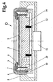
- the pressing of the lower sealing ring against the upper sealing ring may alternatively take place by means of the union nut 4 when the device base, with interposed elastic buffer elements 8, as shown in the example of Figures 2 and 3, as Druckkonterpart for the sealing ring 10 is used.
- a bellows seal between the sealing ring 10 and device base is connected in such a case.
- the bellows can be used arbitrarily, vertically or horizontally and is usually made of rubber or rubberized textile material.
- the bellows sealing system when the bellows 9 is designed in a double manner and thereby forms a chamber, can also serve as a channel 14 for pneumatic or hydraulic pressure media for pressing the lower sealing ring 10, as shown in FIG.
- FIG. 1 shows by way of example a device for the prior art.
- the inventive level consists in particular in the vertical system assembly of the inventive device.
- the tension of the assembled system elements is vertical-rectilinear. Accordingly, the assembly of the individual elements can be carried out according to the insertion principle.
Landscapes
- Chemical & Material Sciences (AREA)
- Engineering & Computer Science (AREA)
- Organic Chemistry (AREA)
- Electrochemistry (AREA)
- Materials Engineering (AREA)
- Metallurgy (AREA)
- Chemical Kinetics & Catalysis (AREA)
- Life Sciences & Earth Sciences (AREA)
- Sustainable Development (AREA)
- Automation & Control Theory (AREA)
- Electroplating Methods And Accessories (AREA)
- Electrodes Of Semiconductors (AREA)
- Medicines Containing Plant Substances (AREA)
- Medicinal Preparation (AREA)
- Sealing Battery Cases Or Jackets (AREA)
Claims (7)
- Dispositif de galvanisation destiné à la galvanisation de tranches de silicium composé: d'un support pour le dispositif avec filetage intérieur (1), d'un écrou-raccord (4) pour l'attache et la fixation de l'intégralité du système du dispositif, d'un adaptateur (5) servant de support de réception pour la tranche de silicium à galvaniser et d'éléments étanches servant à étancher la zone d'électrolyte,
caractérisé en ce que :le dispositif de galvanisation possède un anneau étanche supérieur (3) sur les deux faces duquel est situé un évidemment destiné à recevoir des joints toriques insérés, l'un se trouvant sur la face supérieure de l'anneau étanche pour recevoir le joint torique (6) et l'autre se trouvant sur la face inférieure de l'anneau étanche pour recevoir le joint torique (7), que le dispositif de galvanisation possède un autre anneau étanche inférieur (10) ayant la forme d'un anneau ou d'un disque disposant chacun d'un contre-évidement positionné en face de l'évidement de l'anneau étanche supérieur (3) et destiné à recevoir le joint torique inférieur (7) et que l'anneau étanche (3) et les éléments étanches (10) sont insérés dans le support (1) ou la partie intermédiaire (16) sans jeu latéral pressant ainsi les joints toriques (6) et (7) l'un contre l'autre pour garantir une zone close et étanche à l'électrolyte. - Dispositif selon la revendication 1, caractérisé en ce que
la compression de l'un des éléments étanches (10) contre l'anneau étanche (3), joints toriques insérés, s'effectue au moyen de systèmes de pression pneumatique voire hydraulique. - Dispositif selon les revendications 1 et 2, caractérisé en ce que,
lors de l'utilisation des systèmes de pression pneumatique ou hydraulique avec un anneau étanche (10) et un joint torique (7) inséré en tant que contrepartie inférieure à l'anneau étanche (3), l'alimentation en fluide de pression hydraulique ou pneumatique s'effectue par le biais d'un canal continu (14) composé d'un soufflet double (15) étanche. - Dispositif selon les revendications 1 et 2, caractérisé en ce que,
lors de l'utilisation des systèmes de pression pneumatique avec un disque étanche (10) et un joint torique (7) inséré en tant que contrepartie inférieure à l'anneau étanche (3), l'alimentation en fluide de pression hydraulique voire pneumatique s'effectue en fonction de la surface sur une membrane flexible (17), ce qui permet de presser l'anneau étanche (3) et le disque étanche (10) l'un contre l'autre de manière dynamique et intégralement homogène. - Dispositif selon les revendications 1 et 3 et 4, caractérisé en ce que,
l'alimentation régulée en fluide de pression s'effectue par le biais d'une unité de régulation qui respecte le domaine de charge des joints toriques de telle manière que les joints toriques ne sont pas déformés, ce qui garantit une étanchéité optimale. - Dispositif selon la revendication 1, caractérisé en ce que,
les amortisseurs de soutien (8) et (12) sont utilisés pour amortir la charge à laquelle sont soumis les joints toriques lors de la tension et pour favoriser une configuration différentiable en hauteur du dispositif. - Dispositif selon la revendication 1, caractérisé en ce que,
des systèmes de soufflet (9) sont utilisés pour étancher la zone d'électrolyte dans les différentes possibilités de configuration du dispositif.
Applications Claiming Priority (2)
| Application Number | Priority Date | Filing Date | Title |
|---|---|---|---|
| DE10333068A DE10333068A1 (de) | 2003-07-19 | 2003-07-19 | Scheibengalvanikvorrichtung |
| DE10333068 | 2003-07-19 |
Publications (3)
| Publication Number | Publication Date |
|---|---|
| EP1510601A1 EP1510601A1 (fr) | 2005-03-02 |
| EP1510601B1 EP1510601B1 (fr) | 2006-03-01 |
| EP1510601B9 true EP1510601B9 (fr) | 2006-11-15 |
Family
ID=34042003
Family Applications (1)
| Application Number | Title | Priority Date | Filing Date |
|---|---|---|---|
| EP04016833A Expired - Lifetime EP1510601B9 (fr) | 2003-07-19 | 2004-07-16 | appareil de placage de wafer |
Country Status (6)
| Country | Link |
|---|---|
| US (1) | US20050045473A1 (fr) |
| EP (1) | EP1510601B9 (fr) |
| CN (1) | CN100339511C (fr) |
| AT (1) | ATE318945T1 (fr) |
| CA (1) | CA2474830A1 (fr) |
| DE (2) | DE10333068A1 (fr) |
Families Citing this family (3)
| Publication number | Priority date | Publication date | Assignee | Title |
|---|---|---|---|---|
| US20130306465A1 (en) * | 2012-05-17 | 2013-11-21 | Applied Materials, Inc. | Seal rings in electrochemical processors |
| JP6713916B2 (ja) * | 2016-12-01 | 2020-06-24 | 株式会社荏原製作所 | 基板ホルダ、めっき装置、及び基板ホルダの製造方法 |
| CN109158713B (zh) * | 2018-09-27 | 2024-05-07 | 格林美(武汉)城市矿产循环产业园开发有限公司 | 一种继电器螺纹微镀修复定位装置 |
Family Cites Families (14)
| Publication number | Priority date | Publication date | Assignee | Title |
|---|---|---|---|---|
| US5405518A (en) * | 1994-04-26 | 1995-04-11 | Industrial Technology Research Institute | Workpiece holder apparatus |
| JP3578811B2 (ja) * | 1994-10-12 | 2004-10-20 | シチズン時計株式会社 | 半導体ウエハーのメッキ方法 |
| US5578167A (en) * | 1996-01-31 | 1996-11-26 | Motorola, Inc. | Substrate holder and method of use |
| JP3106418B2 (ja) * | 1996-07-30 | 2000-11-06 | 株式会社東京精密 | 研磨装置 |
| JP3366193B2 (ja) * | 1996-09-10 | 2003-01-14 | ヤマハ発動機株式会社 | 表面処理装置におけるシール装置 |
| US6080291A (en) * | 1998-07-10 | 2000-06-27 | Semitool, Inc. | Apparatus for electrochemically processing a workpiece including an electrical contact assembly having a seal member |
| US6248222B1 (en) * | 1998-09-08 | 2001-06-19 | Acm Research, Inc. | Methods and apparatus for holding and positioning semiconductor workpieces during electropolishing and/or electroplating of the workpieces |
| US6228233B1 (en) * | 1998-11-30 | 2001-05-08 | Applied Materials, Inc. | Inflatable compliant bladder assembly |
| DE19923871C2 (de) * | 1999-05-25 | 2003-11-13 | Rossendorf Forschzent | Einrichtung zur abgedichteten Halterung dünner Scheiben |
| US6673216B2 (en) * | 1999-08-31 | 2004-01-06 | Semitool, Inc. | Apparatus for providing electrical and fluid communication to a rotating microelectronic workpiece during electrochemical processing |
| JP2001158993A (ja) * | 1999-11-30 | 2001-06-12 | Honda Motor Co Ltd | 筒状部材のメッキ装置 |
| JP2001260065A (ja) * | 2000-03-17 | 2001-09-25 | Advantest Corp | 部品保持装置 |
| US6685815B2 (en) * | 2002-01-14 | 2004-02-03 | Applied Materials Inc. | Electroplating of semiconductor wafers |
| US7147232B2 (en) * | 2003-06-30 | 2006-12-12 | Hydra-Lock Corporation | Workpiece holder |
-
2003
- 2003-07-19 DE DE10333068A patent/DE10333068A1/de not_active Withdrawn
-
2004
- 2004-07-16 DE DE502004000318T patent/DE502004000318D1/de not_active Expired - Lifetime
- 2004-07-16 EP EP04016833A patent/EP1510601B9/fr not_active Expired - Lifetime
- 2004-07-16 AT AT04016833T patent/ATE318945T1/de not_active IP Right Cessation
- 2004-07-16 CA CA002474830A patent/CA2474830A1/fr not_active Abandoned
- 2004-07-19 CN CNB2004100851753A patent/CN100339511C/zh not_active Expired - Fee Related
- 2004-07-19 US US10/894,161 patent/US20050045473A1/en not_active Abandoned
Also Published As
| Publication number | Publication date |
|---|---|
| DE502004000318D1 (de) | 2006-04-27 |
| EP1510601A1 (fr) | 2005-03-02 |
| ATE318945T1 (de) | 2006-03-15 |
| EP1510601B1 (fr) | 2006-03-01 |
| CN1614100A (zh) | 2005-05-11 |
| US20050045473A1 (en) | 2005-03-03 |
| CN100339511C (zh) | 2007-09-26 |
| CA2474830A1 (fr) | 2005-01-19 |
| DE10333068A1 (de) | 2005-02-10 |
Similar Documents
| Publication | Publication Date | Title |
|---|---|---|
| DE60005270T2 (de) | Trägervorrichtung für eine chemisch-mechanische poliervorrichtung, mit einem halterring und einer trägerplatte mit mehrzonaler drucksteuervorrichtung | |
| DE69530801T2 (de) | Montageelement und methode zum klemmen eines flachen, dünnen und leitfähigen werkstückes | |
| DE19859467C2 (de) | Substrathalter | |
| DE10208414B4 (de) | Vorrichtung mit einem verbesserten Polierkissenaufbereiter für das chemisch mechanische Polieren | |
| DE69404745T2 (de) | Elektrode zur Verwendung in Plasma-unterstützten chemischen Ätzprozessen | |
| CH659484A5 (de) | Anordnung zur beschichtung von substraten mittels kathodenzerstaeubung. | |
| DE2926080A1 (de) | Mittel zur trockenschmierung | |
| DE102013105136B4 (de) | Dichtungssystem in einer elektrochemischen prozessvorrichtung | |
| EP2766644A1 (fr) | Bague de glissement d'un dispositif d'étanchéité à bague de glissement ayant des propriétés allongeant sa durée de vie utile, et son procédé de fabrication | |
| EP2985497B1 (fr) | Élément de verrouillage pour une soupape à vide doté d'un joint d'étanchéité injecté sous pression, vulcanisé | |
| EP3592697B1 (fr) | Dispositif et procédé de mise à disposition d'une pluralité de nanofils | |
| EP2152939A1 (fr) | Dispositif et procédé pour la mise en contact électrique de produit plat dans des installations fonctionnant en continu | |
| EP1510601B9 (fr) | appareil de placage de wafer | |
| EP0741804A1 (fr) | Procede et dispositif de metallisation ou d'attaque electrolytiques d'articles a traiter | |
| DE102014004728A1 (de) | Vorrichtung und Verfahren zum Löten von Fügepartnern | |
| DE3435019A1 (de) | Maskenringanordnung fuer roentgenstrahlenlithographie | |
| DE10261306B4 (de) | Haltering mit reduzierter Abnutzungs- und Kontaminationsrate für einen Polierkopf einer CMP-Anlage und Polierkopf und CMP-Vorrichtung mit Haltering | |
| EP1910590A2 (fr) | Dispositif pour traiter des substrats, en particulier pour effectuer un depot electrolytique sur un substrat | |
| DE19605599C1 (de) | Vorrichtung zum Transport von Substraten | |
| DE102009046750A1 (de) | Elektrochemisches Einebnungssystem mit verbesserter Elektrolytströmung | |
| EP1240663A2 (fr) | Dispositif de fixation de substrats | |
| DE102005045717B3 (de) | Träger für ein Substrat | |
| EP1961706B1 (fr) | Dispositif de traitement electrochimique de l'eau | |
| DE102013104469B4 (de) | Vorrichtung zur großflächigen elektrischen und/oder thermischen Kontaktierung eines Wafers | |
| DE102009023769A1 (de) | Verfahren und Vorrichtung zum gesteuerten elektrolytischen Behandeln von dünnen Schichten |
Legal Events
| Date | Code | Title | Description |
|---|---|---|---|
| PUAI | Public reference made under article 153(3) epc to a published international application that has entered the european phase |
Free format text: ORIGINAL CODE: 0009012 |
|
| 17P | Request for examination filed |
Effective date: 20041228 |
|
| AK | Designated contracting states |
Kind code of ref document: A1 Designated state(s): AT BE BG CH CY CZ DE DK EE ES FI FR GB GR HU IE IT LI LU MC NL PL PT RO SE SI SK TR |
|
| AX | Request for extension of the european patent |
Extension state: AL HR LT LV MK |
|
| 17Q | First examination report despatched |
Effective date: 20050429 |
|
| GRAP | Despatch of communication of intention to grant a patent |
Free format text: ORIGINAL CODE: EPIDOSNIGR1 |
|
| GRAS | Grant fee paid |
Free format text: ORIGINAL CODE: EPIDOSNIGR3 |
|
| AKX | Designation fees paid |
Designated state(s): AT BE BG CH CY CZ DE DK EE ES FI FR GB GR HU IE IT LI LU MC NL PL PT RO SE SI SK TR |
|
| GRAA | (expected) grant |
Free format text: ORIGINAL CODE: 0009210 |
|
| AK | Designated contracting states |
Kind code of ref document: B1 Designated state(s): AT BE BG CH CY CZ DE DK EE ES FI FR GB GR HU IE IT LI LU MC NL PL PT RO SE SI SK TR |
|
| PG25 | Lapsed in a contracting state [announced via postgrant information from national office to epo] |
Ref country code: NL Free format text: LAPSE BECAUSE OF FAILURE TO SUBMIT A TRANSLATION OF THE DESCRIPTION OR TO PAY THE FEE WITHIN THE PRESCRIBED TIME-LIMIT Effective date: 20060301 Ref country code: IE Free format text: LAPSE BECAUSE OF FAILURE TO SUBMIT A TRANSLATION OF THE DESCRIPTION OR TO PAY THE FEE WITHIN THE PRESCRIBED TIME-LIMIT Effective date: 20060301 Ref country code: IT Free format text: LAPSE BECAUSE OF FAILURE TO SUBMIT A TRANSLATION OF THE DESCRIPTION OR TO PAY THE FEE WITHIN THE PRESCRIBED TIME-LIMIT;WARNING: LAPSES OF ITALIAN PATENTS WITH EFFECTIVE DATE BEFORE 2007 MAY HAVE OCCURRED AT ANY TIME BEFORE 2007. THE CORRECT EFFECTIVE DATE MAY BE DIFFERENT FROM THE ONE RECORDED. Effective date: 20060301 Ref country code: SI Free format text: LAPSE BECAUSE OF FAILURE TO SUBMIT A TRANSLATION OF THE DESCRIPTION OR TO PAY THE FEE WITHIN THE PRESCRIBED TIME-LIMIT Effective date: 20060301 Ref country code: SK Free format text: LAPSE BECAUSE OF FAILURE TO SUBMIT A TRANSLATION OF THE DESCRIPTION OR TO PAY THE FEE WITHIN THE PRESCRIBED TIME-LIMIT Effective date: 20060301 Ref country code: PL Free format text: LAPSE BECAUSE OF FAILURE TO SUBMIT A TRANSLATION OF THE DESCRIPTION OR TO PAY THE FEE WITHIN THE PRESCRIBED TIME-LIMIT Effective date: 20060301 Ref country code: GB Free format text: LAPSE BECAUSE OF FAILURE TO SUBMIT A TRANSLATION OF THE DESCRIPTION OR TO PAY THE FEE WITHIN THE PRESCRIBED TIME-LIMIT Effective date: 20060301 Ref country code: FI Free format text: LAPSE BECAUSE OF FAILURE TO SUBMIT A TRANSLATION OF THE DESCRIPTION OR TO PAY THE FEE WITHIN THE PRESCRIBED TIME-LIMIT Effective date: 20060301 Ref country code: RO Free format text: LAPSE BECAUSE OF FAILURE TO SUBMIT A TRANSLATION OF THE DESCRIPTION OR TO PAY THE FEE WITHIN THE PRESCRIBED TIME-LIMIT Effective date: 20060301 |
|
| REG | Reference to a national code |
Ref country code: GB Ref legal event code: FG4D Free format text: NOT ENGLISH |
|
| REG | Reference to a national code |
Ref country code: CH Ref legal event code: EP |
|
| REG | Reference to a national code |
Ref country code: IE Ref legal event code: FG4D Free format text: LANGUAGE OF EP DOCUMENT: GERMAN |
|
| REF | Corresponds to: |
Ref document number: 502004000318 Country of ref document: DE Date of ref document: 20060427 Kind code of ref document: P |
|
| PG25 | Lapsed in a contracting state [announced via postgrant information from national office to epo] |
Ref country code: SE Free format text: LAPSE BECAUSE OF FAILURE TO SUBMIT A TRANSLATION OF THE DESCRIPTION OR TO PAY THE FEE WITHIN THE PRESCRIBED TIME-LIMIT Effective date: 20060601 Ref country code: BG Free format text: LAPSE BECAUSE OF FAILURE TO SUBMIT A TRANSLATION OF THE DESCRIPTION OR TO PAY THE FEE WITHIN THE PRESCRIBED TIME-LIMIT Effective date: 20060601 Ref country code: DK Free format text: LAPSE BECAUSE OF FAILURE TO SUBMIT A TRANSLATION OF THE DESCRIPTION OR TO PAY THE FEE WITHIN THE PRESCRIBED TIME-LIMIT Effective date: 20060601 |
|
| PG25 | Lapsed in a contracting state [announced via postgrant information from national office to epo] |
Ref country code: ES Free format text: LAPSE BECAUSE OF FAILURE TO SUBMIT A TRANSLATION OF THE DESCRIPTION OR TO PAY THE FEE WITHIN THE PRESCRIBED TIME-LIMIT Effective date: 20060612 |
|
| PG25 | Lapsed in a contracting state [announced via postgrant information from national office to epo] |
Ref country code: MC Free format text: LAPSE BECAUSE OF NON-PAYMENT OF DUE FEES Effective date: 20060731 Ref country code: BE Free format text: LAPSE BECAUSE OF NON-PAYMENT OF DUE FEES Effective date: 20060731 |
|
| PG25 | Lapsed in a contracting state [announced via postgrant information from national office to epo] |
Ref country code: PT Free format text: LAPSE BECAUSE OF FAILURE TO SUBMIT A TRANSLATION OF THE DESCRIPTION OR TO PAY THE FEE WITHIN THE PRESCRIBED TIME-LIMIT Effective date: 20060801 |
|
| NLV1 | Nl: lapsed or annulled due to failure to fulfill the requirements of art. 29p and 29m of the patents act | ||
| GBV | Gb: ep patent (uk) treated as always having been void in accordance with gb section 77(7)/1977 [no translation filed] |
Effective date: 20060301 |
|
| REG | Reference to a national code |
Ref country code: IE Ref legal event code: FD4D |
|
| PLBE | No opposition filed within time limit |
Free format text: ORIGINAL CODE: 0009261 |
|
| STAA | Information on the status of an ep patent application or granted ep patent |
Free format text: STATUS: NO OPPOSITION FILED WITHIN TIME LIMIT |
|
| 26N | No opposition filed |
Effective date: 20061204 |
|
| REG | Reference to a national code |
Ref country code: GB Ref legal event code: 710B Free format text: EXTENSION APPLICATION: APPLICATION FOR EXTENSION OF THE PERIOD(S) PRESCRIBED BY RULE(S) SCHEDULE 4 PARA 2 FILED ON 20070314 |
|
| EN | Fr: translation not filed | ||
| GBT | Gb: translation of ep patent filed (gb section 77(6)(a)/1977) |
Effective date: 20070621 |
|
| REG | Reference to a national code |
Ref country code: GB Ref legal event code: 9110 Free format text: EXTENSION ALLOWED: PERIOD(S) PRESCRIBED BY RULE(S) SCHEDULE 4 PARA 2 EXTENDED UNDER RULE 110(6) IN ACCORDANCE WITH THE DECISION OF THE COMPTROLLER DATED 20070502. THE PATENT/APPLICATION IS REINSTATED SUBJECT TO SPECIAL TERMS FOR THIRD PARTY INTERESTS. |
|
| PG25 | Lapsed in a contracting state [announced via postgrant information from national office to epo] |
Ref country code: AT Free format text: LAPSE BECAUSE OF NON-PAYMENT OF DUE FEES Effective date: 20060716 |
|
| BERE | Be: lapsed |
Owner name: RENA SONDERMASCHINEN G.M.B.H. Effective date: 20060731 |
|
| PG25 | Lapsed in a contracting state [announced via postgrant information from national office to epo] |
Ref country code: CZ Free format text: LAPSE BECAUSE OF FAILURE TO SUBMIT A TRANSLATION OF THE DESCRIPTION OR TO PAY THE FEE WITHIN THE PRESCRIBED TIME-LIMIT Effective date: 20060301 Ref country code: FR Free format text: LAPSE BECAUSE OF FAILURE TO SUBMIT A TRANSLATION OF THE DESCRIPTION OR TO PAY THE FEE WITHIN THE PRESCRIBED TIME-LIMIT Effective date: 20070309 Ref country code: GR Free format text: LAPSE BECAUSE OF FAILURE TO SUBMIT A TRANSLATION OF THE DESCRIPTION OR TO PAY THE FEE WITHIN THE PRESCRIBED TIME-LIMIT Effective date: 20060602 |
|
| PG25 | Lapsed in a contracting state [announced via postgrant information from national office to epo] |
Ref country code: EE Free format text: LAPSE BECAUSE OF FAILURE TO SUBMIT A TRANSLATION OF THE DESCRIPTION OR TO PAY THE FEE WITHIN THE PRESCRIBED TIME-LIMIT Effective date: 20060301 |
|
| PG25 | Lapsed in a contracting state [announced via postgrant information from national office to epo] |
Ref country code: TR Free format text: LAPSE BECAUSE OF FAILURE TO SUBMIT A TRANSLATION OF THE DESCRIPTION OR TO PAY THE FEE WITHIN THE PRESCRIBED TIME-LIMIT Effective date: 20060301 Ref country code: HU Free format text: LAPSE BECAUSE OF FAILURE TO SUBMIT A TRANSLATION OF THE DESCRIPTION OR TO PAY THE FEE WITHIN THE PRESCRIBED TIME-LIMIT Effective date: 20060902 Ref country code: LU Free format text: LAPSE BECAUSE OF NON-PAYMENT OF DUE FEES Effective date: 20060716 |
|
| PGFP | Annual fee paid to national office [announced via postgrant information from national office to epo] |
Ref country code: CH Payment date: 20080731 Year of fee payment: 5 |
|
| PG25 | Lapsed in a contracting state [announced via postgrant information from national office to epo] |
Ref country code: FR Free format text: LAPSE BECAUSE OF FAILURE TO SUBMIT A TRANSLATION OF THE DESCRIPTION OR TO PAY THE FEE WITHIN THE PRESCRIBED TIME-LIMIT Effective date: 20060301 Ref country code: CY Free format text: LAPSE BECAUSE OF FAILURE TO SUBMIT A TRANSLATION OF THE DESCRIPTION OR TO PAY THE FEE WITHIN THE PRESCRIBED TIME-LIMIT Effective date: 20060301 |
|
| PGFP | Annual fee paid to national office [announced via postgrant information from national office to epo] |
Ref country code: GB Payment date: 20080714 Year of fee payment: 5 |
|
| REG | Reference to a national code |
Ref country code: CH Ref legal event code: PL |
|
| GBPC | Gb: european patent ceased through non-payment of renewal fee |
Effective date: 20090716 |
|
| PG25 | Lapsed in a contracting state [announced via postgrant information from national office to epo] |
Ref country code: CH Free format text: LAPSE BECAUSE OF NON-PAYMENT OF DUE FEES Effective date: 20090731 Ref country code: LI Free format text: LAPSE BECAUSE OF NON-PAYMENT OF DUE FEES Effective date: 20090731 |
|
| PG25 | Lapsed in a contracting state [announced via postgrant information from national office to epo] |
Ref country code: GB Free format text: LAPSE BECAUSE OF NON-PAYMENT OF DUE FEES Effective date: 20090716 |
|
| REG | Reference to a national code |
Ref country code: DE Ref legal event code: R084 Ref document number: 502004000318 Country of ref document: DE |
|
| REG | Reference to a national code |
Ref country code: DE Ref legal event code: R084 Ref document number: 502004000318 Country of ref document: DE |
|
| REG | Reference to a national code |
Ref country code: DE Ref legal event code: R084 Ref document number: 502004000318 Country of ref document: DE Effective date: 20110616 |
|
| PGFP | Annual fee paid to national office [announced via postgrant information from national office to epo] |
Ref country code: DE Payment date: 20140127 Year of fee payment: 10 |
|
| REG | Reference to a national code |
Ref country code: DE Ref legal event code: R119 Ref document number: 502004000318 Country of ref document: DE |
|
| PG25 | Lapsed in a contracting state [announced via postgrant information from national office to epo] |
Ref country code: DE Free format text: LAPSE BECAUSE OF NON-PAYMENT OF DUE FEES Effective date: 20150203 |
|
| REG | Reference to a national code |
Ref country code: DE Ref legal event code: R119 Ref document number: 502004000318 Country of ref document: DE Effective date: 20150203 |