EP1510053B1 - Verfahren und system zur elektromagnetisch kopplung des geräts an einen bus - Google Patents
Verfahren und system zur elektromagnetisch kopplung des geräts an einen bus Download PDFInfo
- Publication number
- EP1510053B1 EP1510053B1 EP03731491A EP03731491A EP1510053B1 EP 1510053 B1 EP1510053 B1 EP 1510053B1 EP 03731491 A EP03731491 A EP 03731491A EP 03731491 A EP03731491 A EP 03731491A EP 1510053 B1 EP1510053 B1 EP 1510053B1
- Authority
- EP
- European Patent Office
- Prior art keywords
- bus
- coupling
- locations
- strengths
- circuit board
- Prior art date
- Legal status (The legal status is an assumption and is not a legal conclusion. Google has not performed a legal analysis and makes no representation as to the accuracy of the status listed.)
- Expired - Lifetime
Links
- 230000008878 coupling Effects 0.000 title claims description 49
- 238000010168 coupling process Methods 0.000 title claims description 49
- 238000005859 coupling reaction Methods 0.000 title claims description 49
- 238000000034 method Methods 0.000 title claims description 19
- 238000004519 manufacturing process Methods 0.000 claims description 8
- 238000004891 communication Methods 0.000 claims description 3
- 125000006850 spacer group Chemical group 0.000 claims description 2
- 230000007246 mechanism Effects 0.000 description 3
- 230000008901 benefit Effects 0.000 description 2
- 230000012447 hatching Effects 0.000 description 2
- 239000002184 metal Substances 0.000 description 2
- 230000004075 alteration Effects 0.000 description 1
- 230000000593 degrading effect Effects 0.000 description 1
- 239000003989 dielectric material Substances 0.000 description 1
- 238000009434 installation Methods 0.000 description 1
- 239000000463 material Substances 0.000 description 1
- 230000035699 permeability Effects 0.000 description 1
- 230000000750 progressive effect Effects 0.000 description 1
- 230000011664 signaling Effects 0.000 description 1
Images
Classifications
-
- H—ELECTRICITY
- H01—ELECTRIC ELEMENTS
- H01P—WAVEGUIDES; RESONATORS, LINES, OR OTHER DEVICES OF THE WAVEGUIDE TYPE
- H01P5/00—Coupling devices of the waveguide type
- H01P5/12—Coupling devices having more than two ports
- H01P5/16—Conjugate devices, i.e. devices having at least one port decoupled from one other port
- H01P5/18—Conjugate devices, i.e. devices having at least one port decoupled from one other port consisting of two coupled guides, e.g. directional couplers
- H01P5/184—Conjugate devices, i.e. devices having at least one port decoupled from one other port consisting of two coupled guides, e.g. directional couplers the guides being strip lines or microstrips
- H01P5/185—Edge coupled lines
-
- H—ELECTRICITY
- H04—ELECTRIC COMMUNICATION TECHNIQUE
- H04L—TRANSMISSION OF DIGITAL INFORMATION, e.g. TELEGRAPHIC COMMUNICATION
- H04L12/00—Data switching networks
- H04L12/28—Data switching networks characterised by path configuration, e.g. LAN [Local Area Networks] or WAN [Wide Area Networks]
- H04L12/40—Bus networks
- H04L12/403—Bus networks with centralised control, e.g. polling
-
- H—ELECTRICITY
- H04—ELECTRIC COMMUNICATION TECHNIQUE
- H04L—TRANSMISSION OF DIGITAL INFORMATION, e.g. TELEGRAPHIC COMMUNICATION
- H04L25/00—Baseband systems
- H04L25/02—Details ; arrangements for supplying electrical power along data transmission lines
- H04L25/0264—Arrangements for coupling to transmission lines
- H04L25/0266—Arrangements for providing Galvanic isolation, e.g. by means of magnetic or capacitive coupling
Definitions
- Electromagnetic couplers can be used, for example, to couple data between electronic devices and a communication bus (e.g., a multi-drop bus) in place of more conventional direct electrical connections.
- a communication bus e.g., a multi-drop bus
- Such an arrangement is proposed in U.S. Pat. No. 5,638,402 .
- An electronic device that communicates data on a bus sends or receives the data in the form of an electrical signal that conforms to a predefined signaling specification.
- the receiving device assumes that the signal conformed to the specification when it was sent.
- US 2001/0006538A1 discloses a method according to the preamble of claim 1 for coupling data between electronic devices and a communication bus.
- the coupling strengths of the couplings between the bus and the communicating devices 24, 26, 28 may all be controlled to be uniformly within a targeted range.
- One way to control the coupling strengths to be uniform is to impose tight manufacturing tolerances on the dimensions and properties of dielectric materials associated with the couplings.
- Another is to use zigzag coupler geometries that reduce the impact on coupling strength of variations in the geometric precision of the coupling arrangements. Zigzag coupling arrangements are described in U.S. patent application Ser. No. 09/714,899, filed Nov. 15,2000 .
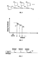
- Controlling coupling strengths to fall uniformly within a particular range achieves a compromise between competing constraints. Excessive coupler strengths cause large impedance disturbances along the bus, thereby degrading signal integrity. High coupler strengths also divert too much signal energy into drop-off points 24 that are closer to the bus master 30, leaving little energy to divert to distant drop-off points 28. On the other hand, insufficient coupler strength causes even the nearest drop-off points to receive or impart too little energy from or to the bus.
- each device along the bus It is useful to arrange for each device along the bus to receive the same amount of energy as any of the other devices along the bus.
- the amount of energy received by a device depends on both the coupling strength and the amount of energy available on the bus at the point of coupling.
- each coupler 42, 44, 46 along the length of the bus drains an amount of energy 41, 43, 45 from the bus.
- the energy drained at coupler 42 leaves a smaller remaining amount 47 of energy to reach the next coupler 44 farther from the bus master.
- the coupling strength must be higher for coupler 44 to drain the same energy 43 as was drained by the prior coupler 42.
- the higher coupling strength of coupler 44 is tolerable because there are fewer downstream couplers that need to draw energy from the bus than was the case for coupler 42.
- weaker earlier couplers are tolerable because the full signal energy is available for them to sample, while the fact that they drain less energy benefits later couplers.
- couplers drawn using longer lines e.g., coupler 54 represent stronger coupling strengths, although physical dimensions are only one way of achieving this.
- Other examples include material properties of the coupler, for example, permittivity and permeability and the extent of the coupler along all three dimensions.
- the configuration of the traces may also be controlled (patterned). For example, besides zig-zags, perforated ground planes and other implementations may be used.
- Coupler strengths along the bus reduces the cost associated with tight manufacturing tolerances, because couplers having a range of different strengths become useful. Yield increases and cost is reduced.
- a variety of mechanisms may be used for introducing and utilizing non-uniform coupler strengths for multi-drop electromagnetically coupled buses.
- the finished couplers may be tested and sorted by coupling strength.
- the relative coupling strengths of the couplers may be indicated by marking the couplers 56 with color 58 or symbols 60 or other indicia or devices. Any device or technique can be used which assures that couplers of the intended strength occupy intended positions along the bus.
- the system may rely on human installation in the right position based on color.
- the placing of the couplers may be effected by robotic systems that could "read” color indications or bar codes or other information marked on the couplers.
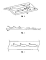
- appropriate positioning of the various couplers may be enforced by providing different keyed mechanical features 62 on the couplers that correspond to the different coupling strengths.
- the motherboard may then be constructed to have corresponding features 66 to accept only a particular coupler key at each position along the bus 68.
- coupler strength may be achieved more deliberately, for example, by controlling dielectric thicknesses, dielectric constants, and the number of zigzag geometry crossover points on the coupling traces of the bus and the coupler.
- the choice among possible mechanisms could be based on cost. For example, if the cost of engineering and manufacturing multiple categories of modules to be attached to the bus is a concern, the system may use uniform daughter cards and make alterations only to parameters of the motherboards that affect the coupling strengths at various points along the bus.
- motherboards may include dielectric spacers 70, 72, 74 of different heights glued to the motherboard 80 at the locations of drop-off points along the bus. Or the widths of motherboard coupling traces 86, 82, 84 may be different at different coupler locations, as shown on figure 6 (also not to scale).
- Wider traces would yield stronger coupling for couplers that are farther away from the bus controller. Wider traces could use either different categories of daughter cards (if the trace width variations were to be provided on the daughter cards rather than on the motherboard) or adjustment of the trace widths on the motherboard.
- the variation in impedance of the motherboard traces could be offset, if desired, by progressive cross hatching.
- the cross-hatching may be in the form of a pattern of holes in the ground plane of the motherboard.
- the removal of metal changes the impedance, because the field lines terminate in different patterns than for continuous metal.
- More cross hatching may be provided under wider traces.
- the cross-hatching maintains the average overlap between the trace and the ground plane, which factors into the trace impedance, thus removing any unwanted correlation between the strength of a coupler and its standalone impedance to its own ground plane.
Landscapes
- Engineering & Computer Science (AREA)
- Computer Networks & Wireless Communication (AREA)
- Signal Processing (AREA)
- Power Engineering (AREA)
- Structure Of Printed Boards (AREA)
- Near-Field Transmission Systems (AREA)
- Gas-Insulated Switchgears (AREA)
- Dc Digital Transmission (AREA)
Claims (18)
- Verfahren, welches Folgendes umfasst:Bereitstellen von Orten (12, 14, 16) elektromagnetischer Kopplung an Kopplungsspuren (82, 84, 86) entlang eines Busses (10), an welchen Geräte (24, 26, 28) jeweils für eine Kommunikation auf dem Bus (10) gekoppelt werden können, undBewirken, dass mit zumindest einigen Kopplungsorten (12, 14, 16) verbundene elektromagnetische Kopplungsstärken unterschiedliche, ausgewählte Werte aufweisen, wobei das Verfahren durch die folgenden weiteren Schritte gekennzeichnet ist:Anordnen des Busses (10) entlang einer Platine (80); undKonfigurieren innerer Ebenen innerhalb der Platine (80), um mit den verschiedenen Kopplungsorten (12, 14, 16) verbundene Impedanzunterschiede entlang des Busses (10) auszugleichen, beinhaltend ein Bereitstellen eines Musters von Löchern in einer Grundebene der Platine (80) zum Aufrechterhalten eines durchschnittlichen Überlapps zwischen den Kopplungsspuren (82, 84, 86) auf der Platine (80) und der Grundebene.
- Verfahren nach Anspruch 1, wobei das Bewirken ein Erwirken von Unterschieden in physikalischen Kenngrößen von Elementen von zumindest einigen an den Kopplungsorten befindlichen Kopplungselementen (42, 44, 46) umfasst.
- Verfahren nach Anspruch 1, wobei das Bewirken ein Messen elektromagnetischer Kopplungsstärken von Kopplungselementen (42, 44, 46), welche dazu dienen, an den Kopplungsorten verwendet zu werden, und ein Bewirken, dass die Kopplungselemente mit unterschiedlichen gemessenen elektromagnetischen Kopplungsstärken ausgewählte Kopplungsorte besetzen, umfasst.
- Verfahren nach Anspruch 1, wobei die unterschiedlichen elektromagnetischen Kopplungsstärken von den physikalischen Kenngrößen von an dem Bus (10) angebrachten Kopplungselementen (42, 44, 46) oder durch die physikalischen Kenngrößen des Busses (10) oder durch beides bewirkt wird.
- Verfahren nach Anspruch 2, wobei die physikalischen Kenngrößen Abmessungen umfassen.
- Verfahren nach Anspruch 2, wobei die physikalischen Kenngrößen von Variationen herrühren, welche innerhalb von Herstellungstoleranzen auftreten.
- Verfahren nach Anspruch 2, wobei die physikalischen Kenngrößen eine Kopplungselementegeometrie umfassen.
- Verfahren nach Anspruch 7, wobei die Geometrie Zickzackspuren aufweist.
- Verfahren nach Anspruch 2, wobei die physikalischen Kenngrößen dielektrische Kenngrößen umfassen.
- Verfahren nach Anspruch 1, wobei bewirkt wird, dass die elektromagnetischen Kopplungsstärken monoton entlang des Busses (10) zunehmen oder abnehmen.
- Verfahren nach Anspruch 1, wobei bewirkt wird, dass die Stärken an den Orten Werte aufweisen, so dass an den jeweiligen Orten (12, 14, 16) im Wesentlichen gleiche Energiemengen von dem Bus (10) abfließen.
- Verfahren nach Anspruch 10, wobei das Zunehmen von einem Ende des Busses (10), welches dem Verbinden mit einer Signalquelle dient, her geschieht.
- Verfahren nach Anspruch 12, wobei die Signalquelle einen Bus-Master (30) umfasst.
- Verfahren nach Anspruch 1, welches weiter ein Bereitstellen von Markierungen (58, 60) auf Elementen (56), welche die Kopplungsstärken beeinflussen, und ein Plazieren der Elemente (56) an Orten entlang des Busses (10) auf Grundlage der Markierungen umfasst.
- Verfahren nach Anspruch 14, wobei das Plazieren von Hand erfolgt.
- System, welches Folgendes umfasst:eine Platine (80), welche einen Bus (10) trägt, undan Kopplungsorten (12, 14, 16) entlang des Busses angeordnete Buselemente, welche mit unterschiedlichen, ausgewählten Kopplungsstärken zum Koppeln mit kommunizierenden Geräten (24, 26, 28) verbunden sind,dadurch gekennzeichnet, dassdie Buselemente Kopplungsspuren (82, 84, 86) umfassen, unddass ein Muster von Löchern in einer Grundebene der Platine (80) bereitgestellt ist,um einen durchschnittlichen Überlapp zwischen den Kopplungsspuren (82, 84, 86) auf der Platine (80) und der Grundebene aufrechtzuerhalten.
- System nach Anspruch 16, wobei die Kopplungsspuren (82, 84, 86) unterschiedliche Abmessungen aufweisen.
- System nach Anspruch 16, wobei die Buselemente dielektrische Abstandshalter (70, 72, 74) umfassen.
Applications Claiming Priority (3)
| Application Number | Priority Date | Filing Date | Title |
|---|---|---|---|
| US10/165,096 US7126437B2 (en) | 2002-06-05 | 2002-06-05 | Bus signaling through electromagnetic couplers having different coupling strengths at different locations |
| US165096 | 2002-06-05 | ||
| PCT/US2003/017314 WO2003105427A1 (en) | 2002-06-05 | 2003-05-30 | Method and system for electromagnetically coupling devices to a bus |
Publications (2)
| Publication Number | Publication Date |
|---|---|
| EP1510053A1 EP1510053A1 (de) | 2005-03-02 |
| EP1510053B1 true EP1510053B1 (de) | 2012-07-11 |
Family
ID=29710359
Family Applications (1)
| Application Number | Title | Priority Date | Filing Date |
|---|---|---|---|
| EP03731491A Expired - Lifetime EP1510053B1 (de) | 2002-06-05 | 2003-05-30 | Verfahren und system zur elektromagnetisch kopplung des geräts an einen bus |
Country Status (6)
| Country | Link |
|---|---|
| US (1) | US7126437B2 (de) |
| EP (1) | EP1510053B1 (de) |
| CN (1) | CN1675905B (de) |
| AU (1) | AU2003240483A1 (de) |
| TW (1) | TWI224736B (de) |
| WO (1) | WO2003105427A1 (de) |
Families Citing this family (11)
| Publication number | Priority date | Publication date | Assignee | Title |
|---|---|---|---|---|
| US20030152153A1 (en) * | 2002-02-14 | 2003-08-14 | Simon Thomas D. | Signaling through electromagnetic couplers |
| US7075795B2 (en) * | 2002-02-14 | 2006-07-11 | Intel Corporation | Electromagnetic bus coupling |
| US7088198B2 (en) * | 2002-06-05 | 2006-08-08 | Intel Corporation | Controlling coupling strength in electromagnetic bus coupling |
| US7068120B2 (en) | 2002-06-25 | 2006-06-27 | Intel Corporation | Electromagnetic bus coupling having an electromagnetic coupling interposer |
| TWI242132B (en) * | 2002-07-01 | 2005-10-21 | Renesas Tech Corp | Equal-amplitude directional coupling bus system |
| US6887095B2 (en) * | 2002-12-30 | 2005-05-03 | Intel Corporation | Electromagnetic coupler registration and mating |
| DE102004032513B4 (de) * | 2004-07-06 | 2013-04-04 | Continental Teves Ag & Co. Ohg | Schaltungsanordnung zum kontaktlosen Abgreifen von elektrischen Signalen von mindestens einer Signalleitung |
| US7830225B2 (en) * | 2005-06-13 | 2010-11-09 | Gale Robert D | Electric signal splitters |
| US7375533B2 (en) * | 2005-06-15 | 2008-05-20 | Gale Robert D | Continuity tester adaptors |
| US7342466B2 (en) * | 2005-08-10 | 2008-03-11 | Intel Corporation | Hybrid coupler having resistive coupling and electromagnetic coupling |
| CN101853825B (zh) * | 2009-04-03 | 2012-01-25 | 鸿富锦精密工业(深圳)有限公司 | 多负载拓扑架构 |
Family Cites Families (32)
| Publication number | Priority date | Publication date | Assignee | Title |
|---|---|---|---|---|
| US18526A (en) * | 1857-10-27 | Steam-pressure gkage | ||
| US3516065A (en) | 1967-01-13 | 1970-06-02 | Ibm | Digital transmission system |
| FR1548848A (de) | 1967-01-13 | 1968-12-06 | ||
| US3673548A (en) | 1970-10-19 | 1972-06-27 | Itt | Printed circuit board connector |
| US4192832A (en) * | 1979-01-29 | 1980-03-11 | Goettl Adam D | Automatic flushing and draining reservoir apparatus for evaporative coolers |
| US5192832A (en) | 1990-08-31 | 1993-03-09 | Amp Incorporated | Electromagnet insert for data current coupler |
| US5363071A (en) * | 1993-05-04 | 1994-11-08 | Motorola, Inc. | Apparatus and method for varying the coupling of a radio frequency signal |
| US5432486A (en) | 1993-05-20 | 1995-07-11 | Northern Telecom Limited | Capacitive and inductive coupling connector |
| JP3399630B2 (ja) | 1993-09-27 | 2003-04-21 | 株式会社日立製作所 | バスシステム |
| CN2286322Y (zh) * | 1996-12-13 | 1998-07-15 | 李曦 | 色环电阻直读卡 |
| US5958030A (en) | 1996-12-27 | 1999-09-28 | Nortel Networks Corporation | Intra-shelf free space interconnect |
| AUPO546797A0 (en) * | 1997-03-05 | 1997-03-27 | Commonwealth Scientific And Industrial Research Organisation | A high frequency multi-port switching circuit |
| JP3543555B2 (ja) | 1997-08-08 | 2004-07-14 | 株式会社日立製作所 | 信号伝送装置 |
| US6111476A (en) * | 1998-12-21 | 2000-08-29 | Nortel Networks Corporation | Non-contact coupling system |
| JP3820843B2 (ja) | 1999-05-12 | 2006-09-13 | 株式会社日立製作所 | 方向性結合式メモリモジュール |
| US6625682B1 (en) | 1999-05-25 | 2003-09-23 | Intel Corporation | Electromagnetically-coupled bus system |
| US6697420B1 (en) | 1999-05-25 | 2004-02-24 | Intel Corporation | Symbol-based signaling for an electromagnetically-coupled bus system |
| US6498305B1 (en) | 1999-05-25 | 2002-12-24 | Intel Corporation | Interconnect mechanics for electromagnetic coupler |
| US6576847B2 (en) * | 1999-05-25 | 2003-06-10 | Intel Corporation | Clamp to secure carrier to device for electromagnetic coupler |
| US6449308B1 (en) | 1999-05-25 | 2002-09-10 | Intel Corporation | High-speed digital distribution system |
| US6434647B1 (en) | 1999-05-27 | 2002-08-13 | Microsoft Corporation | Reflected-wave bus termination |
| US6335662B1 (en) * | 1999-09-21 | 2002-01-01 | The United States Of America As Represented By The Secretary Of The Army | Ferroelectric-tunable microwave branching couplers |
| US6399898B1 (en) | 1999-11-18 | 2002-06-04 | Nortel Networks Limited | Technique for coupling signals between circuit boards |
| TW530248B (en) | 2000-08-09 | 2003-05-01 | Hitachi Ltd | Data transmission system of directional coupling type using forward wave and reflective wave |
| DE10055090A1 (de) | 2000-11-07 | 2002-05-08 | Conducta Endress & Hauser | Steckverbinder zum Anschluss einer Übertragungsleitung an mindestens einen Sensor |
| US6573801B1 (en) | 2000-11-15 | 2003-06-03 | Intel Corporation | Electromagnetic coupler |
| US6437647B1 (en) * | 2001-01-30 | 2002-08-20 | Conexant Systems, Inc. | Current mirror compensation system for power amplifiers |
| US6882239B2 (en) | 2001-05-08 | 2005-04-19 | Formfactor, Inc. | Electromagnetically coupled interconnect system |
| US20030152153A1 (en) | 2002-02-14 | 2003-08-14 | Simon Thomas D. | Signaling through electromagnetic couplers |
| US7075795B2 (en) | 2002-02-14 | 2006-07-11 | Intel Corporation | Electromagnetic bus coupling |
| US7088198B2 (en) | 2002-06-05 | 2006-08-08 | Intel Corporation | Controlling coupling strength in electromagnetic bus coupling |
| US7068120B2 (en) | 2002-06-25 | 2006-06-27 | Intel Corporation | Electromagnetic bus coupling having an electromagnetic coupling interposer |
-
2002
- 2002-06-05 US US10/165,096 patent/US7126437B2/en not_active Expired - Fee Related
-
2003
- 2003-05-30 CN CN03818822.8A patent/CN1675905B/zh not_active Expired - Fee Related
- 2003-05-30 AU AU2003240483A patent/AU2003240483A1/en not_active Abandoned
- 2003-05-30 EP EP03731491A patent/EP1510053B1/de not_active Expired - Lifetime
- 2003-05-30 WO PCT/US2003/017314 patent/WO2003105427A1/en not_active Ceased
- 2003-06-03 TW TW092115082A patent/TWI224736B/zh not_active IP Right Cessation
Also Published As
| Publication number | Publication date |
|---|---|
| TW200407714A (en) | 2004-05-16 |
| WO2003105427A1 (en) | 2003-12-18 |
| US7126437B2 (en) | 2006-10-24 |
| AU2003240483A1 (en) | 2003-12-22 |
| CN1675905B (zh) | 2010-12-08 |
| EP1510053A1 (de) | 2005-03-02 |
| CN1675905A (zh) | 2005-09-28 |
| US20030227346A1 (en) | 2003-12-11 |
| TWI224736B (en) | 2004-12-01 |
Similar Documents
| Publication | Publication Date | Title |
|---|---|---|
| EP1510053B1 (de) | Verfahren und system zur elektromagnetisch kopplung des geräts an einen bus | |
| DE69838364T2 (de) | Schreib-/Lesevorrichtung, Stromversorgungssystem und Kommunikationssystem | |
| DE102008051948B4 (de) | Integrierte-Schaltung-Bauelement, das eine kontaktlose integrierte Schaltung-Einlage umfasst | |
| EP1686649B1 (de) | Mäanderförmige Antenne | |
| CN101743666B (zh) | 无线标签以及无线标签的制造方法 | |
| DE10196914B4 (de) | Elektromagnetischer Koppler | |
| DE102010024439B4 (de) | Antennenvorrichtung | |
| JP2003522386A (ja) | 高速圧力装着コネクタ | |
| KR100860448B1 (ko) | 면상 코일 부품, 면상 코일 부품의 특성 조정 방법,id태그, 및 id태그의 특성 조정 방법 | |
| DE112009002384B4 (de) | Antenne und Drahtlose-IC-Bauelement | |
| EP2333691B1 (de) | Verbindungskabel zur elektrischen oder Lichtwellenleiterverbindung zweier Systemgeräte | |
| CN104078745A (zh) | 天线装置 | |
| EP1939793B1 (de) | Passives RF-Detektierplättchen | |
| WO2011157883A1 (en) | Method for manufacturing an autocompensating antenna structure by etching | |
| DE102012110170B4 (de) | Modulares Bussystem zur Übertragung von Daten und/oder Energie | |
| EP3070636A1 (de) | Lesefeldindikator zur prüfung des lesefeldes eines rfid-lesegerätes | |
| CA2060840A1 (en) | Printed-circuit board | |
| DE602006001034T2 (de) | Funkübertragungssystem, Antennenvorrichtung und Verfahren zur Bogenbearbeitung | |
| EP2959427B1 (de) | Lese/schreibeinrichtung für chipkarten | |
| JP2000306049A (ja) | 無線カード処理装置 | |
| EP1054467B1 (de) | Verfahren zur Einstellung des Koppelfaktors eines Streifenleitungsrichtkopplers und Streifenleitungsrichtkoppler | |
| CN211182498U (zh) | 一种基于rfid的档案架近场盘点天线 | |
| CN103036002A (zh) | 传感设备 | |
| CN207474674U (zh) | 基于可调频段的工业遥控器缩小天线 | |
| DE102006059444B4 (de) | RFID-Marke |
Legal Events
| Date | Code | Title | Description |
|---|---|---|---|
| PUAI | Public reference made under article 153(3) epc to a published international application that has entered the european phase |
Free format text: ORIGINAL CODE: 0009012 |
|
| 17P | Request for examination filed |
Effective date: 20041111 |
|
| AK | Designated contracting states |
Kind code of ref document: A1 Designated state(s): AT BE BG CH CY CZ DE DK EE ES FI FR GB GR HU IE IT LI LU MC NL PT RO SE SI SK TR |
|
| AX | Request for extension of the european patent |
Extension state: AL LT LV MK |
|
| RIN1 | Information on inventor provided before grant (corrected) |
Inventor name: BENHAM, JOHN Inventor name: AMIRTHARAJAH, RAJEEVAN Inventor name: SIMON, THOMAS |
|
| DAX | Request for extension of the european patent (deleted) | ||
| 17Q | First examination report despatched |
Effective date: 20100706 |
|
| REG | Reference to a national code |
Ref country code: DE Ref legal event code: R079 Ref document number: 60341516 Country of ref document: DE Free format text: PREVIOUS MAIN CLASS: H04L0025020000 Ipc: H01P0005180000 |
|
| RIC1 | Information provided on ipc code assigned before grant |
Ipc: H04L 12/403 20060101ALI20111104BHEP Ipc: H01P 5/18 20060101AFI20111104BHEP Ipc: H04L 25/02 20060101ALI20111104BHEP |
|
| GRAP | Despatch of communication of intention to grant a patent |
Free format text: ORIGINAL CODE: EPIDOSNIGR1 |
|
| GRAS | Grant fee paid |
Free format text: ORIGINAL CODE: EPIDOSNIGR3 |
|
| GRAA | (expected) grant |
Free format text: ORIGINAL CODE: 0009210 |
|
| AK | Designated contracting states |
Kind code of ref document: B1 Designated state(s): AT BE BG CH CY CZ DE DK EE ES FI FR GB GR HU IE IT LI LU MC NL PT RO SE SI SK TR |
|
| REG | Reference to a national code |
Ref country code: GB Ref legal event code: FG4D |
|
| REG | Reference to a national code |
Ref country code: CH Ref legal event code: EP |
|
| REG | Reference to a national code |
Ref country code: AT Ref legal event code: REF Ref document number: 566526 Country of ref document: AT Kind code of ref document: T Effective date: 20120715 |
|
| REG | Reference to a national code |
Ref country code: IE Ref legal event code: FG4D |
|
| REG | Reference to a national code |
Ref country code: DE Ref legal event code: R096 Ref document number: 60341516 Country of ref document: DE Effective date: 20120830 |
|
| REG | Reference to a national code |
Ref country code: NL Ref legal event code: VDEP Effective date: 20120711 |
|
| REG | Reference to a national code |
Ref country code: AT Ref legal event code: MK05 Ref document number: 566526 Country of ref document: AT Kind code of ref document: T Effective date: 20120711 |
|
| PG25 | Lapsed in a contracting state [announced via postgrant information from national office to epo] |
Ref country code: AT Free format text: LAPSE BECAUSE OF FAILURE TO SUBMIT A TRANSLATION OF THE DESCRIPTION OR TO PAY THE FEE WITHIN THE PRESCRIBED TIME-LIMIT Effective date: 20120711 Ref country code: BE Free format text: LAPSE BECAUSE OF FAILURE TO SUBMIT A TRANSLATION OF THE DESCRIPTION OR TO PAY THE FEE WITHIN THE PRESCRIBED TIME-LIMIT Effective date: 20120711 Ref country code: FI Free format text: LAPSE BECAUSE OF FAILURE TO SUBMIT A TRANSLATION OF THE DESCRIPTION OR TO PAY THE FEE WITHIN THE PRESCRIBED TIME-LIMIT Effective date: 20120711 Ref country code: CY Free format text: LAPSE BECAUSE OF FAILURE TO SUBMIT A TRANSLATION OF THE DESCRIPTION OR TO PAY THE FEE WITHIN THE PRESCRIBED TIME-LIMIT Effective date: 20120711 |
|
| PG25 | Lapsed in a contracting state [announced via postgrant information from national office to epo] |
Ref country code: PT Free format text: LAPSE BECAUSE OF FAILURE TO SUBMIT A TRANSLATION OF THE DESCRIPTION OR TO PAY THE FEE WITHIN THE PRESCRIBED TIME-LIMIT Effective date: 20121112 Ref country code: SI Free format text: LAPSE BECAUSE OF FAILURE TO SUBMIT A TRANSLATION OF THE DESCRIPTION OR TO PAY THE FEE WITHIN THE PRESCRIBED TIME-LIMIT Effective date: 20120711 Ref country code: SE Free format text: LAPSE BECAUSE OF FAILURE TO SUBMIT A TRANSLATION OF THE DESCRIPTION OR TO PAY THE FEE WITHIN THE PRESCRIBED TIME-LIMIT Effective date: 20120711 Ref country code: GR Free format text: LAPSE BECAUSE OF FAILURE TO SUBMIT A TRANSLATION OF THE DESCRIPTION OR TO PAY THE FEE WITHIN THE PRESCRIBED TIME-LIMIT Effective date: 20121012 |
|
| PG25 | Lapsed in a contracting state [announced via postgrant information from national office to epo] |
Ref country code: NL Free format text: LAPSE BECAUSE OF FAILURE TO SUBMIT A TRANSLATION OF THE DESCRIPTION OR TO PAY THE FEE WITHIN THE PRESCRIBED TIME-LIMIT Effective date: 20120711 |
|
| PG25 | Lapsed in a contracting state [announced via postgrant information from national office to epo] |
Ref country code: ES Free format text: LAPSE BECAUSE OF FAILURE TO SUBMIT A TRANSLATION OF THE DESCRIPTION OR TO PAY THE FEE WITHIN THE PRESCRIBED TIME-LIMIT Effective date: 20121022 Ref country code: EE Free format text: LAPSE BECAUSE OF FAILURE TO SUBMIT A TRANSLATION OF THE DESCRIPTION OR TO PAY THE FEE WITHIN THE PRESCRIBED TIME-LIMIT Effective date: 20120711 Ref country code: CZ Free format text: LAPSE BECAUSE OF FAILURE TO SUBMIT A TRANSLATION OF THE DESCRIPTION OR TO PAY THE FEE WITHIN THE PRESCRIBED TIME-LIMIT Effective date: 20120711 Ref country code: DK Free format text: LAPSE BECAUSE OF FAILURE TO SUBMIT A TRANSLATION OF THE DESCRIPTION OR TO PAY THE FEE WITHIN THE PRESCRIBED TIME-LIMIT Effective date: 20120711 Ref country code: RO Free format text: LAPSE BECAUSE OF FAILURE TO SUBMIT A TRANSLATION OF THE DESCRIPTION OR TO PAY THE FEE WITHIN THE PRESCRIBED TIME-LIMIT Effective date: 20120711 |
|
| PLBE | No opposition filed within time limit |
Free format text: ORIGINAL CODE: 0009261 |
|
| STAA | Information on the status of an ep patent application or granted ep patent |
Free format text: STATUS: NO OPPOSITION FILED WITHIN TIME LIMIT |
|
| PG25 | Lapsed in a contracting state [announced via postgrant information from national office to epo] |
Ref country code: IT Free format text: LAPSE BECAUSE OF FAILURE TO SUBMIT A TRANSLATION OF THE DESCRIPTION OR TO PAY THE FEE WITHIN THE PRESCRIBED TIME-LIMIT Effective date: 20120711 Ref country code: SK Free format text: LAPSE BECAUSE OF FAILURE TO SUBMIT A TRANSLATION OF THE DESCRIPTION OR TO PAY THE FEE WITHIN THE PRESCRIBED TIME-LIMIT Effective date: 20120711 |
|
| 26N | No opposition filed |
Effective date: 20130412 |
|
| PG25 | Lapsed in a contracting state [announced via postgrant information from national office to epo] |
Ref country code: BG Free format text: LAPSE BECAUSE OF FAILURE TO SUBMIT A TRANSLATION OF THE DESCRIPTION OR TO PAY THE FEE WITHIN THE PRESCRIBED TIME-LIMIT Effective date: 20121011 |
|
| REG | Reference to a national code |
Ref country code: DE Ref legal event code: R097 Ref document number: 60341516 Country of ref document: DE Effective date: 20130412 |
|
| PG25 | Lapsed in a contracting state [announced via postgrant information from national office to epo] |
Ref country code: MC Free format text: LAPSE BECAUSE OF FAILURE TO SUBMIT A TRANSLATION OF THE DESCRIPTION OR TO PAY THE FEE WITHIN THE PRESCRIBED TIME-LIMIT Effective date: 20120711 |
|
| REG | Reference to a national code |
Ref country code: CH Ref legal event code: PL |
|
| PG25 | Lapsed in a contracting state [announced via postgrant information from national office to epo] |
Ref country code: CH Free format text: LAPSE BECAUSE OF NON-PAYMENT OF DUE FEES Effective date: 20130531 Ref country code: LI Free format text: LAPSE BECAUSE OF NON-PAYMENT OF DUE FEES Effective date: 20130531 |
|
| REG | Reference to a national code |
Ref country code: IE Ref legal event code: MM4A |
|
| REG | Reference to a national code |
Ref country code: FR Ref legal event code: ST Effective date: 20140131 |
|
| PG25 | Lapsed in a contracting state [announced via postgrant information from national office to epo] |
Ref country code: IE Free format text: LAPSE BECAUSE OF NON-PAYMENT OF DUE FEES Effective date: 20130530 |
|
| PG25 | Lapsed in a contracting state [announced via postgrant information from national office to epo] |
Ref country code: FR Free format text: LAPSE BECAUSE OF NON-PAYMENT OF DUE FEES Effective date: 20130531 |
|
| PG25 | Lapsed in a contracting state [announced via postgrant information from national office to epo] |
Ref country code: TR Free format text: LAPSE BECAUSE OF FAILURE TO SUBMIT A TRANSLATION OF THE DESCRIPTION OR TO PAY THE FEE WITHIN THE PRESCRIBED TIME-LIMIT Effective date: 20120711 |
|
| PG25 | Lapsed in a contracting state [announced via postgrant information from national office to epo] |
Ref country code: HU Free format text: LAPSE BECAUSE OF FAILURE TO SUBMIT A TRANSLATION OF THE DESCRIPTION OR TO PAY THE FEE WITHIN THE PRESCRIBED TIME-LIMIT; INVALID AB INITIO Effective date: 20030530 Ref country code: LU Free format text: LAPSE BECAUSE OF NON-PAYMENT OF DUE FEES Effective date: 20130530 |
|
| PGFP | Annual fee paid to national office [announced via postgrant information from national office to epo] |
Ref country code: DE Payment date: 20160524 Year of fee payment: 14 Ref country code: GB Payment date: 20160525 Year of fee payment: 14 |
|
| REG | Reference to a national code |
Ref country code: DE Ref legal event code: R119 Ref document number: 60341516 Country of ref document: DE |
|
| GBPC | Gb: european patent ceased through non-payment of renewal fee |
Effective date: 20170530 |
|
| PG25 | Lapsed in a contracting state [announced via postgrant information from national office to epo] |
Ref country code: GB Free format text: LAPSE BECAUSE OF NON-PAYMENT OF DUE FEES Effective date: 20170530 Ref country code: DE Free format text: LAPSE BECAUSE OF NON-PAYMENT OF DUE FEES Effective date: 20171201 |