EP1510002B1 - Transresistanzverstärker für einen detektor für geladene teilchen - Google Patents
Transresistanzverstärker für einen detektor für geladene teilchen Download PDFInfo
- Publication number
- EP1510002B1 EP1510002B1 EP03727668A EP03727668A EP1510002B1 EP 1510002 B1 EP1510002 B1 EP 1510002B1 EP 03727668 A EP03727668 A EP 03727668A EP 03727668 A EP03727668 A EP 03727668A EP 1510002 B1 EP1510002 B1 EP 1510002B1
- Authority
- EP
- European Patent Office
- Prior art keywords
- transresistance
- transresistance amplifier
- amplifier
- photo
- light
- Prior art date
- Legal status (The legal status is an assumption and is not a legal conclusion. Google has not performed a legal analysis and makes no representation as to the accuracy of the status listed.)
- Expired - Lifetime
Links
- 239000002245 particle Substances 0.000 title claims description 12
- 230000001419 dependent effect Effects 0.000 claims description 30
- 239000003990 capacitor Substances 0.000 claims description 20
- 230000005684 electric field Effects 0.000 claims description 4
- 230000003321 amplification Effects 0.000 claims description 3
- 239000000463 material Substances 0.000 claims description 3
- 238000003199 nucleic acid amplification method Methods 0.000 claims description 3
- CJOBVZJTOIVNNF-UHFFFAOYSA-N cadmium sulfide Chemical compound [Cd]=S CJOBVZJTOIVNNF-UHFFFAOYSA-N 0.000 claims description 2
- 229910052980 cadmium sulfide Inorganic materials 0.000 claims description 2
- UHYPYGJEEGLRJD-UHFFFAOYSA-N cadmium(2+);selenium(2-) Chemical compound [Se-2].[Cd+2] UHYPYGJEEGLRJD-UHFFFAOYSA-N 0.000 claims description 2
- 230000005669 field effect Effects 0.000 claims description 2
- 239000000872 buffer Substances 0.000 description 8
- 238000002955 isolation Methods 0.000 description 4
- 238000010586 diagram Methods 0.000 description 3
- 230000003139 buffering effect Effects 0.000 description 2
- 238000009499 grossing Methods 0.000 description 2
- 238000005286 illumination Methods 0.000 description 2
- 230000002238 attenuated effect Effects 0.000 description 1
- 238000006880 cross-coupling reaction Methods 0.000 description 1
- 230000000630 rising effect Effects 0.000 description 1
- 230000035945 sensitivity Effects 0.000 description 1
Images





Classifications
-
- H—ELECTRICITY
- H01—ELECTRIC ELEMENTS
- H01J—ELECTRIC DISCHARGE TUBES OR DISCHARGE LAMPS
- H01J37/00—Discharge tubes with provision for introducing objects or material to be exposed to the discharge, e.g. for the purpose of examination or processing thereof
- H01J37/02—Details
- H01J37/244—Detectors; Associated components or circuits therefor
-
- H—ELECTRICITY
- H01—ELECTRIC ELEMENTS
- H01J—ELECTRIC DISCHARGE TUBES OR DISCHARGE LAMPS
- H01J37/00—Discharge tubes with provision for introducing objects or material to be exposed to the discharge, e.g. for the purpose of examination or processing thereof
- H01J37/26—Electron or ion microscopes; Electron or ion diffraction tubes
- H01J37/261—Details
-
- H—ELECTRICITY
- H03—ELECTRONIC CIRCUITRY
- H03F—AMPLIFIERS
- H03F1/00—Details of amplifiers with only discharge tubes, only semiconductor devices or only unspecified devices as amplifying elements
- H03F1/56—Modifications of input or output impedances, not otherwise provided for
-
- H—ELECTRICITY
- H03—ELECTRONIC CIRCUITRY
- H03F—AMPLIFIERS
- H03F3/00—Amplifiers with only discharge tubes or only semiconductor devices as amplifying elements
- H03F3/04—Amplifiers with only discharge tubes or only semiconductor devices as amplifying elements with semiconductor devices only
- H03F3/08—Amplifiers with only discharge tubes or only semiconductor devices as amplifying elements with semiconductor devices only controlled by light
- H03F3/087—Amplifiers with only discharge tubes or only semiconductor devices as amplifying elements with semiconductor devices only controlled by light with IC amplifier blocks
-
- H—ELECTRICITY
- H03—ELECTRONIC CIRCUITRY
- H03F—AMPLIFIERS
- H03F3/00—Amplifiers with only discharge tubes or only semiconductor devices as amplifying elements
- H03F3/45—Differential amplifiers
- H03F3/45071—Differential amplifiers with semiconductor devices only
- H03F3/45076—Differential amplifiers with semiconductor devices only characterised by the way of implementation of the active amplifying circuit in the differential amplifier
- H03F3/45475—Differential amplifiers with semiconductor devices only characterised by the way of implementation of the active amplifying circuit in the differential amplifier using IC blocks as the active amplifying circuit
-
- H—ELECTRICITY
- H03—ELECTRONIC CIRCUITRY
- H03G—CONTROL OF AMPLIFICATION
- H03G1/00—Details of arrangements for controlling amplification
- H03G1/0005—Circuits characterised by the type of controlling devices operated by a controlling current or voltage signal
- H03G1/0035—Circuits characterised by the type of controlling devices operated by a controlling current or voltage signal using continuously variable impedance elements
- H03G1/0047—Circuits characterised by the type of controlling devices operated by a controlling current or voltage signal using continuously variable impedance elements using photo-electric elements
-
- H—ELECTRICITY
- H03—ELECTRONIC CIRCUITRY
- H03G—CONTROL OF AMPLIFICATION
- H03G3/00—Gain control in amplifiers or frequency changers
- H03G3/20—Automatic control
- H03G3/30—Automatic control in amplifiers having semiconductor devices
- H03G3/3084—Automatic control in amplifiers having semiconductor devices in receivers or transmitters for electromagnetic waves other than radiowaves, e.g. lightwaves
-
- H—ELECTRICITY
- H01—ELECTRIC ELEMENTS
- H01J—ELECTRIC DISCHARGE TUBES OR DISCHARGE LAMPS
- H01J2237/00—Discharge tubes exposing object to beam, e.g. for analysis treatment, etching, imaging
- H01J2237/244—Detection characterized by the detecting means
- H01J2237/2448—Secondary particle detectors
-
- H—ELECTRICITY
- H03—ELECTRONIC CIRCUITRY
- H03F—AMPLIFIERS
- H03F2200/00—Indexing scheme relating to amplifiers
- H03F2200/261—Amplifier which being suitable for instrumentation applications
-
- H—ELECTRICITY
- H03—ELECTRONIC CIRCUITRY
- H03F—AMPLIFIERS
- H03F2203/00—Indexing scheme relating to amplifiers with only discharge tubes or only semiconductor devices as amplifying elements covered by H03F3/00
- H03F2203/45—Indexing scheme relating to differential amplifiers
- H03F2203/45138—Two or more differential amplifiers in IC-block form are combined, e.g. measuring amplifiers
-
- H—ELECTRICITY
- H03—ELECTRONIC CIRCUITRY
- H03F—AMPLIFIERS
- H03F2203/00—Indexing scheme relating to amplifiers with only discharge tubes or only semiconductor devices as amplifying elements covered by H03F3/00
- H03F2203/45—Indexing scheme relating to differential amplifiers
- H03F2203/45512—Indexing scheme relating to differential amplifiers the FBC comprising one or more capacitors, not being switched capacitors, and being coupled between the LC and the IC
-
- H—ELECTRICITY
- H03—ELECTRONIC CIRCUITRY
- H03F—AMPLIFIERS
- H03F2203/00—Indexing scheme relating to amplifiers with only discharge tubes or only semiconductor devices as amplifying elements covered by H03F3/00
- H03F2203/45—Indexing scheme relating to differential amplifiers
- H03F2203/45528—Indexing scheme relating to differential amplifiers the FBC comprising one or more passive resistors and being coupled between the LC and the IC
-
- H—ELECTRICITY
- H03—ELECTRONIC CIRCUITRY
- H03F—AMPLIFIERS
- H03F2203/00—Indexing scheme relating to amplifiers with only discharge tubes or only semiconductor devices as amplifying elements covered by H03F3/00
- H03F2203/45—Indexing scheme relating to differential amplifiers
- H03F2203/45594—Indexing scheme relating to differential amplifiers the IC comprising one or more resistors, which are not biasing resistor
Definitions
- This invention relates to a transresistance amplifier for use in a charged particle detector, to a charged particle detector that includes such a transresistance amplifier, and to an electron microscope that includes such a charged particle detector.
- Charged particle detectors are well known, and typically comprise an electrode, means for establishing an electric field in the vicinity of the electrode so as to attract charged particles towards the electrode, and a transresistance amplifier for converting an input current made up of charged particles incident on the electrode into an output voltage.
- the transresistance amplifier typically comprises an input resistance through which the input current flows so as to develop an input voltage, and a voltage amplifier that receives the input voltage and generates the output voltage.
- the input voltage received by the voltage amplifier inevitably comprises both the signal component developed across the input resistance and a small noise component.
- the magnitude of the noise component is approximately constant, regardless of the magnitude of the signal component. From the point of view of the signal-to-noise ratio of the output voltage, therefore, it is desirable for the input resistance, and hence the input voltage, to be as large as possible.
- the voltage amplifier has some input capacitance, which, together with the input resistance, forms a low-pass filter, the cut-off frequency of which is inversely proportional to the input resistance. From the point of view of the bandwidth of the output voltage, therefore, it is desirable for the input resistance of the amplifier to be as small as possible.
- Prior art transresistance amplifiers are known from e.g., US5670775 and US5311353 .
- transresistance amplifiers have been provided with a voltage amplifier with variable gain and several switchable input resistances, any one of which may be connected, typically by means of a relay, between the electron detector and the voltage amplifier.
- the variable gain of the voltage amplifier is necessary to accommodate the step changes in sensitivity resulting from the use of switchable input resistances.
- a transresistance amplifier for a charged particle detector, the transresistance amplifier comprising a variable input resistance, a voltage amplification stage and control means operable to vary the variable input resistance, wherein the variable input resistance includes a first light-dependent resistance and the control means includes a first variable intensity light source that is optically coupled to the first light-dependent resistance.
- the invention therefore provides a transresistance amplifier the transresistance of which is continuously variable over its range of adjustment, and which avoids the discontinuity of bandwidth of previous transresistance amplifiers using several switchable input resistances.
- the invention provides a transresistance amplifier that is easier to use than previous transresistance amplifiers, since the gain of the voltage amplification stage does not have to be varied, so that a user of a charged particle detector including the transresistance amplifier need concern himself only with adjusting the input resistance.
- the first light-dependent resistance may advantageously comprise a light-dependent resistor made from cadmium sulphide, cadmium selenide or other photoconductive material.
- a change in resistance of such a material in response to a change in intensity of illumination takes several seconds.
- a light-dependent resistor may be used where the variation of the input resistance of the transresistance amplifier is to be carried out manually by a user of the transresistance amplifier, the light-dependent resistor might be unsuitable for use in conjunction with a closed-loop control system, where the slow speed of response might cause instability of the control system.
- the light-dependent resistance may advantageously comprise a photodiode, an element that has a faster speed of response than a light dependent resistor.
- the light-dependent resistance comprises a phototransistor, and most preferably a photo field-effect transistor (photo FET), a channel of which forms the variable input resistance and a gate region of which is optically coupled to the first variable intensity light source.
- the photo FET provides a resistance that is variable typically from approximately 300 ohms to some hundreds of megohms.
- the first variable intensity light source may advantageously comprise a first light-emitting diode (LED).
- LED light-emitting diode
- the first opto-coupler typically has an impedance of some 10 11 ohms of isolation with a capacitance of approximately 2 picofarads between the first LED and the photo FET.
- the transresistance amplifier may advantageously further comprise a second light-dependent resistance, and a second variable intensity light source optically coupled to the second light-dependent resistance, the second light-dependent resistance being electrically connected to the first variable intensity light source, such that variation of the second light-dependent resistance varies a flow of current through the first variable intensity light source.
- the second light-dependent resistance is connected in series with the first variable intensity light source.
- the second light dependent resistance may advantageously comprise a phototransistor, and preferably a photo bipolar junction transistor (photo BJT), a base region of which is optically coupled to the second variable intensity light source.
- photo BJT photo bipolar junction transistor
- the second variable intensity light source may advantageously comprise a second LED.
- the second LED and photo BJT both form parts of a second opto-coupler.
- the second LED and photo BJT give approximately unity current gain, which facilitates control of the input resistance of the transresistance amplifier.
- the second opto-coupler typically provides some 10 11 ohms of isolation and a capacitance of approximately 0.4 picofarads between the second LED and the photo BJT.
- the impedance between the electrode and the control circuit is increased by the isolation impedance of the second opto-coupler and undesired cross-coupling is reduced accordingly.
- the transresistance amplifier further comprises a capacitor electrically connected to the photo BJT so as to form a low-pass filter that passes dc control currents from the photo BJT to the first LED, but attenuates higher frequency noise currents.
- the capacitance between the second LED and photo BJT of the second opto-coupler may be used to form a potential divider with an additional capacitor with a larger capacitance than that of the second opto-coupler, and that the attenuation of higher frequency noise currents is given approximately by the ratio of the capacitances of the second opto-coupler and the additional capacitor.
- the resistance of the photo FET varies exponentially with respect to current flowing through the first LED, which can make manual control of the transresistance of the transresistance amplifier difficult for users.
- the transresistance amplifier may therefore advantageously further comprise a control circuit having input means operable to generate an input signal representative of a required transresistance of the transresistance amplifier, means for generating an output current logarithmically related to the input signal, the control circuit being electrically connected to the first or second LED such that the output current flows through said first or second LED to obtain the required transresistance.
- the input means comprises a digital-to-analogue converter, but a potentiometer could equally well be used.
- a charged particle detector comprising an electrode, means for establishing an electric field in the vicinity of the electrode, and a transresistance amplifier in accordance with the first aspect of the invention.
- an electron microscope comprising a specimen chamber for receiving a specimen, an electron gun, an electron detector in accordance with the second aspect of the invention, and video means operable to receive an output voltage from the transresistance amplifier and to generate therefrom an image of a specimen.
- the transresistance amplifier is contained within the specimen chamber.
- the invention therefore further provides a transresistance amplifier, which, by virtue of its avoidance of the use of switchable input resistances and relays, can be made smaller than has previously been possible, and can therefore be accommodated within the specimen chamber of the electron microscope, thereby reducing the distance that the input current must be transmitted from the electrode to the transresistance amplifier, and hence the level of interference to which the input current is subjected.
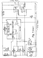
- the amplifier of Figure 1 comprises four stages, a transresistance amplifier, a buffer amplifier, a transconductance amplifier and a photo FET opto-coupler.
- a first low-pass filter is formed by resistor R22 and capacitor C5, and a second low-pass filter by resistor R8 and capacitor C2.
- the first and second low-pass filters smooth the power supply voltage.
- Resistors R9 and R11 form a potential divider that establishes a reference voltage for both the transresistance amplifier and transconductance amplifier.
- Capacitor C3 smoothes the reference voltage.
- the 5 volt power supply for the amplifier floats on a 40 volt power supply.
- a positive terminal of the 40 volt power supply is indicated by TP10 in Figure 1 and is used to establish an electric field in the vicinity of an electrode (not shown) in a specimen chamber of an electron microscope, such that electrons are attracted towards the electrode.
- a negative terminal of the 40 volt power supply is indicated by TP1 and is connected to the chamber (not shown) of the electron microscope (not shown), and to ground.
- Capacitor C10 provides a low impedance path to ground for high frequency noise at the negative terminal of the 5 volt power supply.
- Resistor R1 ties the negative terminal of the 5 volt power supply to the positive terminal of the 40 volt power supply.
- the transresistance amplifier is made up of current limiting resistor R4, input resistor R10, photo FET opto-coupler IC3, voltage amplifier IC1, current limiting resistor R7 and capacitors C6 and C7.
- the operation of the transresistance amplifier is as follows.
- the voltage amplifier IC1 has differential inputs, one of which is connected to the junction of the resistors R9 and R11, and the other to the more negative terminals of the input resistor R10 and channel of the photo FET of the opto-coupler IC3.
- the more positive terminals of the input resistor and channel of the photo FET are connected to the junction of the resistors R9 and R11.
- the voltage developed across the parallel arrangement of the input resistor R10 and channel of the photo FET is applied to the differential inputs of the voltage amplifier IC1.
- the resistance of the channel of the photo FET of the opto-coupler IC3 is determined by the intensity of illumination of the LED of the opto-coupler IC3, which itself is determined by the current flowing through the LED. Control of the current through the LED is by means of a control circuit that is described below in relation to Figure 3 .
- the current limiting resistor R7 prevents damage to the LED of the opto-coupler IC3 in the event of the input to the LED circuit, indicated by TP6, being inadvertently short-circuited to the positive terminal of either power supply.
- Capacitors C7 and C6 attenuate noise coupled into the circuit containing the LED of the opto-coupler IC3.
- the current limiting resistor R4 limits the current that can be drawn from the 5 volt power supply in the event of the electrode becoming short-circuited to the grounded chamber of the electron microscope.
- the lower of the two diodes designated in Figure 1 by D4 goes into conduction, preventing the differential input to the transresistance amplifier from exceeding one forward diode voltage drop.
- the upper of the two diodes designated in Figure 1 by D4 goes into conduction, again so as to prevent the differential input to the transresistance amplifier from exceeding one forward diode voltage drop.
- the diode D3 prevents the reference voltage from dropping more than one forward diode voltage drop below the negative terminal of the power supply, and the diode D2 prevents the reference voltage from rising more than one forward diode voltage drop above the positive terminal of the power supply.
- the buffer amplifier is made up of two unity gain operational amplifiers, both of which are designated IC2 in Figure 1 because they are formed as a single integrated circuit to improve their thermal tracking.
- the upper operational amplifier buffers the output voltage from the transresistance amplifier, and the lower operational amplifier buffers the reference voltage.
- the transconductance amplifier is made up of first and second operational amplifiers, both of which are designated IC6 in Figure 1 because they are formed as a single integrated circuit, a first biasing network comprising resistors R20, R23, and R5 together with smoothing capacitor C9, a second biasing network comprising resistors R12, R19, and R15 together with smoothing capacitor C1, first and second feedback resistors R2 and R16 respectively, and load resistor R14.
- the first biasing network forms a potential divider between the buffered reference voltage and the negative terminal of the 5 volt power supply, the voltage developed across resistors R20 and R23 being applied to the inverting input of the upper operational amplifier.
- the second biasing network forms a potential divider between the output of the first low-pass filter and the buffered output voltage from the transresistance amplifier, the voltage developed across resistor R15 being applied to the non-inverting input of the upper operational amplifier.
- the buffering of the output and reference voltages by the buffer amplifier ensures that the bias voltages applied to the upper operational amplifier of the transconductance amplifier by the first and second biasing networks are not affected by the output and reference voltages.
- the output voltage of the upper operational amplifier is applied to a first terminal of the load resistor R14 so as to produce the output current of the transconductance amplifier.
- a second terminal of the load resistor R14 is connected to the non-inverting input of the lower operational amplifier IC6.
- the lower operational amplifier buffers the voltage at the second terminal of the load resistor R14, so as to ensure that the bias voltage at the non-inverting input of the upper operational amplifier is not affected by the voltage developed across the load resistor R14.
- the LED of the photo BJT opto-coupler IC4 receives the output current of the transconductance amplifier via the current limiting resistor R3, which serves the same purpose as the current limiting resistor R7. A current of magnitude equal to that which flows through the LED flows through the photo BJT of the opto-coupler IC4.
- the photo BJT opto-coupler IC4 is used because of its unity current gain.
- the current flowing through the photo BJT flows through an input resistance (not shown) across which a voltage is developed for application to the input of a video amplifier (not shown).
- the current gain of the opto-coupler IC4 is not unity when the current through the LED is zero. For this reason the bias voltages are applied to the inputs of the upper operational amplifier of the transconductance amplifier, so that even when no signal is present at the input to the transresistance amplifier, there is nevertheless an output current from the transconductance amplifier, resulting in an output voltage at the input to the video amplifier that sets the "black” or no signal level, and thereby preserves the unity current gain of the opto-coupler over the signal range in which it is used.
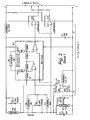
- this also comprises a transresistance amplifier, a buffer amplifier, a transconductance amplifier and a photo BJT opto-coupler.
- the buffer amplifier, transconductance amplifier and photo BJT opto-coupler are identical with those of the amplifier of Figure 1 .
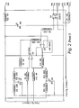
- the transresistance amplifier shown in Figure 2 comprises, in addition to those elements that make up the transresistance amplifier shown in Figure 1 , a photo BJT opto-coupler IC5 and a capacitor C8.
- the photo BJT of the opto-coupler IC5 is connected between the positive terminal of the 5 volt power supply and the anode of the LED of the opto-coupler IC3.
- the cathode of the LED of the opto-coupler IC3 is connected to the negative terminal of the 5 volt power supply.
- the capacitor C8 is connected between the junction of the photo BJT of the opto-coupler IC5 and the anode of the LED of the opto-coupler IC3, and the negative terminal of the 5 volt power supply.
- a control current applied to the input TP6 to the circuit containing the LED of the opto-coupler IC5 causes a current of equal magnitude to flow through the photo BJT of opto-coupler IC5 and LED of opto-coupler IC3, which current controls the resistance of the channel of the photo FET of opto-coupler IC3, as previously described.
- control circuit comprises a digital-to-analogue converter (DAC) (not shown in Figure 3 ), a voltage amplifier, a logarithmic amplifier and a transconductance amplifier.
- DAC digital-to-analogue converter
- the control circuit is supplied by -5 and +5 volt power supplies.
- the voltage amplifier is made up of operational amplifier IC7, first biasing network comprising resistors R23 and R25, and second biasing network comprising resistors R24 and R26.
- Capacitor C11 smoothes the bias voltage at the inverting input of the operational amplifier IC7, and capacitors C12 and C13 smooth the power supply voltages.
- the logarithmic amplifier is made up of a logarithmic amplifier integrated circuit (IC) IC8 and a biasing network comprising resistors R27, R28 and R29.
- Capacitor C14 smoothes the bias voltage at the inverting input of the logarithmic amplifier IC IC8.
- the transconductance amplifier comprises an operational amplifier IC9, first biasing network comprising resistors R30 and R32, second biasing network comprising resistors R31 and R33, and load resistor R34.
- Capacitor C15 smoothes the bias voltage at the inverting input of the operational amplifier IC9, and capacitors C16 and C17 smooth the power supply voltages.
- the DAC supplies a 0 to 5 volt control voltage to the non-inverting input of the operational amplifier IC7 of the voltage amplifier.
- the operational amplifier generates a 0 to -2 volt output voltage proportional to the control voltage.
- the logarithmic amplifier has a bias voltage of -10 millivolts applied to its inverting input by the biasing network comprising resistors R27, R28 and R29, and the non-inverting input is connected to ground.
- the output of the voltage amplifier is connected to a control voltage input of the logarithmic amplifier IC IC8, which produces an output voltage logarithmically related to the control voltage.
- the output voltage from the logarithmic amplifier IC IC8 is connected to the inverting input of the transconductance amplifier, which produces an output current through the load resistor R34 that is logarithmically related to the control voltage.
- the load resistor is connected to the cathode of the LED of the opto-coupler IC5 of the amplifier of Figure 2 , or to the cathode of the LED of the opto-coupler IC3 of the amplifier of Figure 1 , via TP3.
- the anode of the LED in each case is connected to ground via TP6.
Landscapes
- Engineering & Computer Science (AREA)
- Power Engineering (AREA)
- Chemical & Material Sciences (AREA)
- Analytical Chemistry (AREA)
- Physics & Mathematics (AREA)
- Electromagnetism (AREA)
- Amplifiers (AREA)
Claims (19)
- Transresistanz-Verstärker für einen Detektor für geladene Teilchen, wobei der Transresistanz-Verstärker eine variable Eingangsresistanz, eine Spannungsverstärkerstufe (IC1) und Steuermittel umfaßt, die betätigt werden können, um die variable Eingangsresistanz zu variieren, wobei die variable Eingangsresistanz eine erste lichtabhängige Resistanz (IC3) enthält und das Steuermittel eine erste Lichtquelle (IC3) mit variabler Intensität enthält, die optisch an die erste lichtabhängige Resistanz gekoppelt ist.
- Transresistanz-Verstärker nach Anspruch 1, wobei die erste lichtabhängige Resistanz einen lichtabhängigen Widerstand umfaßt, der aus Cadmiumsulfid, Cadmiumselenid oder einem anderen photoleitenden Material hergestellt ist.
- Transresistanz-Verstärker nach Anspruch 1, wobei die lichtabhängige Resistanz eine Photodiode umfaßt.
- Transresistanz-Verstärker nach Anspruch 1, wobei die lichtabhängige Resistanz einen Phototransistor umfaßt.
- Verstärker nach Anspruch 4, wobei der Phototransistor ein Photo-Feldeffekttransistor (Photo-FET) ist, von dem ein Kanal die variable Eingangsresistanz bildet und von dem ein Gategebiet optisch an die erste Lichtquelle mit variabler Intensität gekoppelt ist.
- Verstärker nach einem vorhergehenden Anspruch, wobei die erste Lichtquelle mit variabler Intensität eine erste Leuchtdiode (LED) umfaßt.
- Verstärker nach Anspruch 6, wenn abhängig von Anspruch 5, wobei sowohl die erste LED als auch der Photo-FET Teile eines ersten Optokopplers bilden.
- Transresistanz-Verstärker nach einem vorhergehenden Anspruch, wobei der Transresistanz-Verstärker weiterhin eine zweite lichtabhängige Resistanz umfaßt und eine zweite Lichtquelle mit variabler Intensität optisch an die zweite lichtabhängige Resistanz gekoppelt ist, wobei die zweite lichtabhängige Resistanz elektrisch an die erste Lichtquelle mit variabler Intensität angeschlossen ist, so daß eine Variation der zweiten lichtabhängigen Resistanz einen Stromfluß durch die erste Lichtquelle mit variabler Intensität variiert.
- Transresistanz-Verstärker nach Anspruch 8, wobei die zweite lichtabhängige Resistanz in Reihe mit der ersten Lichtquelle mit variabler Intensität geschaltet ist.
- Transresistanz-Verstärker nach Anspruch 8 oder Anspruch 9, wobei die zweite lichtabhängige Resistanz einen Phototransistor umfaßt.
- Transresistanz-Verstärker nach Anspruch 10, wobei die zweite lichtabhängige Resistanz einen bipolaren Photosperrschichttransistor (Photo-BJT) umfaßt, von dem ein Basisgebiet optisch an die zweite Lichtquelle mit variabler Intensität gekoppelt ist.
- Transresistanz-Verstärker nach einem der Ansprüche 8 bis 11, wobei die zweite Lichtquelle mit variabler Intensität eine zweite LED umfaßt.
- Transresistanz-Verstärker nach Anspruch 12, wenn abhängig von Anspruch 11, wobei sowohl die zweite LED als auch der Photo-BJT Teile eines zweiten Optokopplers bilden.
- Transresistanz-Verstärker nach einem der Ansprüche 11 bis 13, wobei der Transresistanz-Verstärker weiterhin einen Kondensator umfaßt, der elektrisch an den Photo-BJT angeschlossen ist, um ein Tiefpaßfilter zu bilden, das DC-Steuerströme von dem Photo-BJT zu der ersten LED durchläßt, aber höher frequente Rauschströme dämpft.
- Transresistanz-Verstärker nach einem vorhergehenden Anspruch, wobei der Transresistanz-Verstärker weiterhin eine Steuerschaltung mit Eingangsmitteln umfaßt, die betätigt werden können, um ein Eingangssignal zu generieren, das für eine erforderliche Transresistanz des Transresistanz-Verstärkers repräsentativ ist, Mittel zum Generieren eines Ausgangsstroms, der logarithmisch zu dem Eingangssignal in Beziehung steht, wobei die Steuerschaltung elektrisch an die erste oder zweite LED angeschlossen ist, so daß der Ausgangsstrom durch die erste oder zweite LED fließt, um die erforderliche Transresistanz zu erhalten.
- Transresistanz-Verstärker nach Anspruch 15, wobei das Eingangsmittel einen Digital-Analog-Wandler umfaßt.
- Detektor für geladene Teilchen, der eine Elektrode, Mittel zum Herstellen eines elektrischen Felds in der Nähe der Elektrode und einen Transresistanz-Verstärker nach einem vorhergehenden Anspruch umfaßt.
- Elektronenmikroskop, das eine Probenkammer zum Aufnehmen einer Probe, eine Elektronenkanone, einen Elektronendetektor nach Anspruch 17 und Videomittel umfaßt, die betätigt werden können, um eine Ausgangsspannung von dem Transresistanz-Verstärker zu empfangen und daraus ein Bild einer Probe zu generieren.
- Elektronenmikroskop nach Anspruch 18, wobei der Transresistanz-Verstärker in der Probenkammer enthalten ist.
Applications Claiming Priority (3)
| Application Number | Priority Date | Filing Date | Title |
|---|---|---|---|
| GB0212601 | 2002-05-31 | ||
| GB0212601A GB2389260B (en) | 2002-05-31 | 2002-05-31 | Transresistance amplifier for a charged particle detector |
| PCT/GB2003/002089 WO2003103138A1 (en) | 2002-05-31 | 2003-05-15 | Transresistance amplifier for a charged particle detector |
Publications (2)
| Publication Number | Publication Date |
|---|---|
| EP1510002A1 EP1510002A1 (de) | 2005-03-02 |
| EP1510002B1 true EP1510002B1 (de) | 2010-08-11 |
Family
ID=9937794
Family Applications (1)
| Application Number | Title | Priority Date | Filing Date |
|---|---|---|---|
| EP03727668A Expired - Lifetime EP1510002B1 (de) | 2002-05-31 | 2003-05-15 | Transresistanzverstärker für einen detektor für geladene teilchen |
Country Status (5)
| Country | Link |
|---|---|
| US (1) | US7317350B2 (de) |
| EP (1) | EP1510002B1 (de) |
| DE (1) | DE60333750D1 (de) |
| GB (1) | GB2389260B (de) |
| WO (1) | WO2003103138A1 (de) |
Families Citing this family (6)
| Publication number | Priority date | Publication date | Assignee | Title |
|---|---|---|---|---|
| US9403172B2 (en) * | 2012-11-08 | 2016-08-02 | Berkeley Lights, Inc. | Circuit based optoelectronic tweezers |
| US20150346148A1 (en) * | 2014-05-28 | 2015-12-03 | Agilent Technologies, Inc. | Method and Apparatus for Manipulating Samples Using Optoelectronic Forces |
| SG11201708429WA (en) | 2015-04-22 | 2017-11-29 | Berkeley Lights Inc | Microfluidic cell culture |
| US10799865B2 (en) | 2015-10-27 | 2020-10-13 | Berkeley Lights, Inc. | Microfluidic apparatus having an optimized electrowetting surface and related systems and methods |
| CN115678773A (zh) | 2016-05-26 | 2023-02-03 | 伯克利之光生命科技公司 | 共价修饰的表面、试剂盒及制备方法和用途 |
| SG11202104544WA (en) | 2018-11-19 | 2021-06-29 | Berkeley Lights Inc | Microfluidic device with programmable switching elements |
Family Cites Families (9)
| Publication number | Priority date | Publication date | Assignee | Title |
|---|---|---|---|---|
| US3379991A (en) * | 1967-05-15 | 1968-04-23 | Milton C. Clerc | Automatic gain control employing photoresistors |
| GB1435143A (en) * | 1973-06-16 | 1976-05-12 | Ass Elect Ind | Scanning electron microscopes |
| JPS585371B2 (ja) * | 1974-11-20 | 1983-01-31 | 株式会社ニコン | ソツコウヒヨウジカイロ |
| DE2815150A1 (de) * | 1978-04-07 | 1979-10-18 | Agfa Gevaert Ag | Fokussiervorrichtung fuer fotografische oder kinematografische kameras |
| DE3607688A1 (de) * | 1986-03-08 | 1987-09-17 | Kolbe & Co Hans | Empfaenger (empfangsmodul) fuer eine optische nachrichtenuebertragungsstrecke |
| US5623284A (en) * | 1995-04-18 | 1997-04-22 | Elan Microelectronics Corporation | Input device controller |
| US5949225A (en) * | 1998-03-19 | 1999-09-07 | Astec International Limited | Adjustable feedback circuit for adaptive opto drives |
| GB2388236A (en) * | 2002-05-01 | 2003-11-05 | Cambridge Display Tech Ltd | Display and driver circuits |
| EP1367630B1 (de) * | 2002-05-31 | 2011-09-14 | Carl Zeiss SMT Limited | Verbesserungen in einem Teilchendetektor |
-
2002
- 2002-05-31 GB GB0212601A patent/GB2389260B/en not_active Expired - Fee Related
-
2003
- 2003-05-15 DE DE60333750T patent/DE60333750D1/de not_active Expired - Lifetime
- 2003-05-15 WO PCT/GB2003/002089 patent/WO2003103138A1/en not_active Ceased
- 2003-05-15 US US10/515,213 patent/US7317350B2/en not_active Expired - Fee Related
- 2003-05-15 EP EP03727668A patent/EP1510002B1/de not_active Expired - Lifetime
Also Published As
| Publication number | Publication date |
|---|---|
| EP1510002A1 (de) | 2005-03-02 |
| US7317350B2 (en) | 2008-01-08 |
| US20050264351A1 (en) | 2005-12-01 |
| WO2003103138A1 (en) | 2003-12-11 |
| GB2389260B (en) | 2006-03-29 |
| DE60333750D1 (de) | 2010-09-23 |
| GB0212601D0 (en) | 2002-07-10 |
| GB2389260A (en) | 2003-12-03 |
Similar Documents
| Publication | Publication Date | Title |
|---|---|---|
| US5455705A (en) | Transimpedance amplifier for optical receiver | |
| US4327319A (en) | Active power supply ripple filter | |
| US6114913A (en) | Transimpedance amplifiers with improved gain-bandwidth product | |
| JP2538938B2 (ja) | 光前置増幅器 | |
| EP0370608A1 (de) | Temperaturstabilisierter optischer Vorverstärker | |
| US3968361A (en) | Laser receiver anti-sun circuit | |
| EP1510002B1 (de) | Transresistanzverstärker für einen detektor für geladene teilchen | |
| US4889985A (en) | Combined optical power meter and receiver | |
| US4827133A (en) | Infrared space surveillance detector circuit | |
| US6201446B1 (en) | Adaptive bandwidth stabilization for an integrated circuit amplifier | |
| DE10351593B4 (de) | Integrierte Vorverstärkerschaltung für die Erfassung eines Signalstroms von einer Photodiode | |
| US4053847A (en) | Self-feedback type low-noise charge sensitive amplifier | |
| EP0828344A2 (de) | Integrierte Schaltung und Verfahren zur Generierung einer Transimpedanzfunktion | |
| WO2005119908A1 (en) | High pass filter using insulated gate field effect transistors | |
| EP4407509A1 (de) | Logarithmischer strom-spannungswandler mit emitterwiderstandskompensation | |
| EP0460273A1 (de) | Verstärkungsstabilisierter Verstärker | |
| NL8520066A (nl) | Inrichting voor het vergroten van het dynamische gebied bij een integrerende opto-elektrische ontvanger. | |
| EP0368510B1 (de) | Stromverstärker | |
| KR920000572B1 (ko) | 주파수 선택성 비디오 신호 처리 장치 | |
| JPH0846444A (ja) | 帰還増幅回路 | |
| KR940000262B1 (ko) | 주신호통로와 하이패스필터특성의 보조적인 신호통로를 가지는 노이즈 감소회로 | |
| CN222049087U (zh) | 光电传感器 | |
| US20210159858A1 (en) | Transimpedance amplifier circuit | |
| JP7259625B2 (ja) | トランスインピーダンス増幅回路 | |
| Angural et al. | Balanced homodyne detection circuit design analysis for high gain and low noise performance |
Legal Events
| Date | Code | Title | Description |
|---|---|---|---|
| PUAI | Public reference made under article 153(3) epc to a published international application that has entered the european phase |
Free format text: ORIGINAL CODE: 0009012 |
|
| 17P | Request for examination filed |
Effective date: 20041026 |
|
| AK | Designated contracting states |
Kind code of ref document: A1 Designated state(s): AT BE BG CH CY CZ DE DK EE ES FI FR GB GR HU IE IT LI LU MC NL PT RO SE SI SK TR |
|
| AX | Request for extension of the european patent |
Extension state: AL LT LV MK |
|
| DAX | Request for extension of the european patent (deleted) | ||
| RBV | Designated contracting states (corrected) |
Designated state(s): CZ DE GB NL |
|
| RAP1 | Party data changed (applicant data changed or rights of an application transferred) |
Owner name: CARL ZEISS SMT LIMITED |
|
| GRAP | Despatch of communication of intention to grant a patent |
Free format text: ORIGINAL CODE: EPIDOSNIGR1 |
|
| GRAS | Grant fee paid |
Free format text: ORIGINAL CODE: EPIDOSNIGR3 |
|
| GRAA | (expected) grant |
Free format text: ORIGINAL CODE: 0009210 |
|
| AK | Designated contracting states |
Kind code of ref document: B1 Designated state(s): CZ DE GB NL |
|
| REG | Reference to a national code |
Ref country code: GB Ref legal event code: FG4D |
|
| REG | Reference to a national code |
Ref country code: NL Ref legal event code: T3 |
|
| REF | Corresponds to: |
Ref document number: 60333750 Country of ref document: DE Date of ref document: 20100923 Kind code of ref document: P |
|
| PG25 | Lapsed in a contracting state [announced via postgrant information from national office to epo] |
Ref country code: CZ Free format text: LAPSE BECAUSE OF FAILURE TO SUBMIT A TRANSLATION OF THE DESCRIPTION OR TO PAY THE FEE WITHIN THE PRESCRIBED TIME-LIMIT Effective date: 20100811 |
|
| PLBE | No opposition filed within time limit |
Free format text: ORIGINAL CODE: 0009261 |
|
| STAA | Information on the status of an ep patent application or granted ep patent |
Free format text: STATUS: NO OPPOSITION FILED WITHIN TIME LIMIT |
|
| 26N | No opposition filed |
Effective date: 20110512 |
|
| REG | Reference to a national code |
Ref country code: DE Ref legal event code: R097 Ref document number: 60333750 Country of ref document: DE Effective date: 20110512 |
|
| REG | Reference to a national code |
Ref country code: DE Ref legal event code: R082 Ref document number: 60333750 Country of ref document: DE Representative=s name: LOESENBECK UND KOLLEGEN, DE |
|
| REG | Reference to a national code |
Ref country code: DE Ref legal event code: R081 Ref document number: 60333750 Country of ref document: DE Owner name: CARL ZEISS MICROSCOPY LTD., GB Free format text: FORMER OWNER: CARL ZEISS SMT LTD., CAMBRIDGE, GB Effective date: 20111125 Ref country code: DE Ref legal event code: R082 Ref document number: 60333750 Country of ref document: DE Representative=s name: LOESENBECK UND KOLLEGEN, DE Effective date: 20111125 |
|
| REG | Reference to a national code |
Ref country code: DE Ref legal event code: R082 Ref document number: 60333750 Country of ref document: DE Representative=s name: LOESENBECK UND KOLLEGEN, DE |
|
| REG | Reference to a national code |
Ref country code: DE Ref legal event code: R082 Ref document number: 60333750 Country of ref document: DE Representative=s name: LOESENBECK UND KOLLEGEN, DE Effective date: 20130417 Ref country code: DE Ref legal event code: R081 Ref document number: 60333750 Country of ref document: DE Owner name: CARL ZEISS MICROSCOPY LTD., GB Free format text: FORMER OWNER: CARL ZEISS NTS LTD., CAMBRIDGE, GB Effective date: 20130417 |
|
| PGFP | Annual fee paid to national office [announced via postgrant information from national office to epo] |
Ref country code: GB Payment date: 20140521 Year of fee payment: 12 |
|
| PGFP | Annual fee paid to national office [announced via postgrant information from national office to epo] |
Ref country code: NL Payment date: 20140521 Year of fee payment: 12 Ref country code: DE Payment date: 20140521 Year of fee payment: 12 |
|
| REG | Reference to a national code |
Ref country code: DE Ref legal event code: R119 Ref document number: 60333750 Country of ref document: DE |
|
| GBPC | Gb: european patent ceased through non-payment of renewal fee |
Effective date: 20150515 |
|
| REG | Reference to a national code |
Ref country code: NL Ref legal event code: MM Effective date: 20150601 |
|
| PG25 | Lapsed in a contracting state [announced via postgrant information from national office to epo] |
Ref country code: GB Free format text: LAPSE BECAUSE OF NON-PAYMENT OF DUE FEES Effective date: 20150515 Ref country code: DE Free format text: LAPSE BECAUSE OF NON-PAYMENT OF DUE FEES Effective date: 20151201 Ref country code: NL Free format text: LAPSE BECAUSE OF NON-PAYMENT OF DUE FEES Effective date: 20150601 |