EP1508916B1 - Apparatus for cooling semiconductor devices attached to a printed circuit board - Google Patents
Apparatus for cooling semiconductor devices attached to a printed circuit board Download PDFInfo
- Publication number
- EP1508916B1 EP1508916B1 EP03018046A EP03018046A EP1508916B1 EP 1508916 B1 EP1508916 B1 EP 1508916B1 EP 03018046 A EP03018046 A EP 03018046A EP 03018046 A EP03018046 A EP 03018046A EP 1508916 B1 EP1508916 B1 EP 1508916B1
- Authority
- EP
- European Patent Office
- Prior art keywords
- circuit board
- printed circuit
- spring
- cooling
- semiconductor device
- Prior art date
- Legal status (The legal status is an assumption and is not a legal conclusion. Google has not performed a legal analysis and makes no representation as to the accuracy of the status listed.)
- Expired - Lifetime
Links
Images

Classifications
-
- H—ELECTRICITY
- H01—ELECTRIC ELEMENTS
- H01L—SEMICONDUCTOR DEVICES NOT COVERED BY CLASS H10
- H01L23/00—Details of semiconductor or other solid state devices
- H01L23/34—Arrangements for cooling, heating, ventilating or temperature compensation ; Temperature sensing arrangements
- H01L23/42—Fillings or auxiliary members in containers or encapsulations selected or arranged to facilitate heating or cooling
- H01L23/433—Auxiliary members in containers characterised by their shape, e.g. pistons
-
- H—ELECTRICITY
- H01—ELECTRIC ELEMENTS
- H01L—SEMICONDUCTOR DEVICES NOT COVERED BY CLASS H10
- H01L23/00—Details of semiconductor or other solid state devices
- H01L23/34—Arrangements for cooling, heating, ventilating or temperature compensation ; Temperature sensing arrangements
- H01L23/40—Mountings or securing means for detachable cooling or heating arrangements ; fixed by friction, plugs or springs
- H01L23/4006—Mountings or securing means for detachable cooling or heating arrangements ; fixed by friction, plugs or springs with bolts or screws
-
- H—ELECTRICITY
- H01—ELECTRIC ELEMENTS
- H01L—SEMICONDUCTOR DEVICES NOT COVERED BY CLASS H10
- H01L2924/00—Indexing scheme for arrangements or methods for connecting or disconnecting semiconductor or solid-state bodies as covered by H01L24/00
- H01L2924/0001—Technical content checked by a classifier
- H01L2924/0002—Not covered by any one of groups H01L24/00, H01L24/00 and H01L2224/00
Definitions
- the present invention relates to an apparatus for cooling semiconductor devices, such as integrated circuits, mounted on a printed circuit board or the like.
- the heat radiation to cool the semiconductor device is effected by heat transfer from the surface of the heated portion to the surrounding air. Namely, if the resistance of heat transfer between the surface of the heated element and the surrounding air is low, then the heat is well transferred. Therefore, by lowering the heat transfer resistance to the air, better cooling of the heated element is effected. In order to lower the heat transfer resistance to the air, the method to enlarge the surface in contact with the air, i.e. the surface area, has so far been employed.
- reference numeral 104 denotes an integrated circuit, IC.
- the one shown in FIG. 1 is of Dual-In-Line package type but could be of any other type of housing applicable with semiconductor devices.
- Reference numeral 102 denotes a radiating fin, which is made of metal such as copper, aluminum, or the like, having good heat conductivity, and the radiating fin is provided with fine grooves 102a on the top face thereof to magnify the surface area in contact with the air.
- the radiating fin 102 is attached to the top face of the IC 104, a semiconductor device, by means of adhesive, or nuts and bolts. The heat generated by the IC 104 is thus conducted to the radiating fin 102 for cooling.
- the direction of the grooves 102a to magnify the surface area of the radiating fin 102 must be in the direction of the air flow.
- the direction of the IC 104 to be mounted on the printed circuit board is restricted to be in one direction.
- the wiring pattern on the printed circuit board is also subject to restriction.
- the means used for attaching the radiating fin 102 to IC 104 involves problems.
- the means for attaching the radiating fin 102 to IC 104 must endure thermal stress for a long time, so that the radiating fin 102 is held securely attached to the IC 104 even when subject to vibration or shock.
- said means must be adapted such that, under all possible thermal conditions, the semiconductor device does not experience excessive contact pressure resulting from the attaching means.
- first and second heat sink 202, 222 are provided.
- the second heat sink 222 is of cylindrical shape and provided with a thread 222a on the periphery thereof and with a slot 222b on the top face thereof so as to be driven by a screwdriver.
- the first heat sink 202 attached to a shield case 213 is provided with a female thread 202a, so that the threaded heat sink 222 can be engaged therewith.
- the threaded heat sink 222 is adapted to be threadedly engaged with the female thread 202a of the first heat sink 202 from above the shield case 213, to which the heat sink 202 is attached, through a hole 213a.
- the threaded heat sink 222 is passed through the hole 213a at the top of the shield case 213 and threadedly engaged with the threaded portion 202a of the heat sink 202.
- the heat sink 222 is pressed against an IC 204 mounted on a printed circuit board 201.
- a heat conductive rubber 221 with good heat conductivity may be previously attached to the former at its portion which contacts the latter. In such a case, the threaded heat sink 222 contacts with the IC 204 through the rubber 221.
- any variation in the distance (a) between the electronic parts 204 and the heat sink 202 can be minutely compensated with ease by turning the threaded heat sink 222.
- the heat sink 202 and the threaded heat sink 222 are in threaded contact and therefore the surface of contact between them is magnified, so that the heat conducted from the electronic parts 204 through the rubber 221 to the threaded heat sink 222 is easily conducted to the heat sink 202, and emitted to the ambient air through the shield case 213.
- no matter how varied the distances between the first heat sink 202 and the electronic parts 204 may be sufficient pressure of contact and surface of contact for good heat conductivity is always obtained by virtue of the second heat sink 222.
- the conventional apparatus shown in FIG. 2 still exhibits some limitations as, for example, a costly manufacturing process, a multitude of specific parts, and unreasonable weight and height in view of the cooling effect achieved.
- the spring member described in US 2002/0051341A1 is a flat plate fastened at the outer edges of the plate to a substrate. Between the substrate and the spring member a circuit package and a stack of heatpipe for cooling the circuit board are located.
- the spring member is equipped with a dome through which a centering pressure is applied between the cooling stack and the circuit package. Disadvantageous is that the alignment of the stack with respect to the circuit board depends not only on the force applied by the dome but on additional mechanical elements which can cause inhomogeneous pressure between the stack and the circuit board.
- a cartridge including a heat pipe is used as a housing to cover a bottom side of a substrate including a plurality of pins.
- the cartridge is located on the opposite side of the substrate with respect to a spring clip pressing the substrate against the cartridge.
- the force inserted into the substrate by the spring clip can only be influenced by a connection between the cartridge and the spring clip but not by the cartridge itself.
- the present invention discloses an improved apparatus for cooling semiconductor devices attached to a printed circuit board.
- the preferred apparatus for cooling semiconductor devices attached to a printed circuit board comprises: a printed circuit board having first and second sides, said first side having a semiconductor device attached thereto, said printed circuit board further comprises a plurality of apertures formed through said first and second sides; a cooling member adjacent said first side of the printed circuit board and being in thermal contact with the semiconductor device; a spring member adjacent said second side of the printed circuit board; and securing members connecting the spring member to the cooling member through said apertures in the printed circuit board such that the spring member providing a spring force forcing the semiconductor device against the cooling member.
- the present invention provides an apparatus for cooling semiconductor devices attached to a printed circuit board. As shown in FIG. 3 , such printed circuit board 301 is sandwiched between a cooling member established by a cooling plate 302 and a spring member established by a spring plate 303.
- the printed circuit board 301 is a plate of electrically non-conductive material (e. g. resin plate, cermic substrate) comprising at least one structured electrically conductive layer (e g. metallization) for connecting electrical devices such as semiconductor devices.
- the printed circuit board 301 has first and second sides and further comprises a plurality of apertures 305 formed through said first and second sides.
- the first side of the printed circuit board 301 comprises a semiconductor device 304 (e. g. power amplifier, voltage regulator, power switch) attached thereto, e. g. by soldering.
- the printed circuit board 301 comprises a further aperture 309 arranged such that it is covered by the semiconductor device 304.
- the cooling plate 302 is adjacent said first side of the printed circuit board 301 and has first and second sides itself.
- the second side of the cooling plate 302 has thermal contact with the semiconductor device 304.
- a heat conductive means 308, e. g. a thermal compound, may be applied between the semiconductor device 304 and the cooling plate 302.
- electrically insulating means may be provided between the semiconductor device 304 and the cooling plate 302.
- the cooling plate 302 is made of metal and may be provided with fine grooves on the first side thereof to magnify the surface area in contact with the air (not shown in the FIGs.).
- the spring plate 303 is made of metal and arranged adjacent said second side of the printed circuit board 301. It is wave-like embossed such that it comprises a dome 307.
- the dome 307 is located in the further aperture 309 of the printed circuit board 301 and has a height relative to its ground line that exceeds the heights of all other waves or domes due to embossing so that the dome 307 is in direct contact with the semiconductor device 304 and exerting force to the semiconductor device 304 as a result of the spring force provided by the spring plate 303.
- the spring plate 303 comprises apertures 306 corresponding to the apertures 305 of the printed circuit board 301.
- securing members are provided which extend through the apertures 305 of the printed circuit board 301 and the apertures 306 of the spring plate 303.
- the securing members are bolts 310 in connection with integral noses 311 formed in a single piece from the cooling plate 302.
- the integral noses 311 extend partly into the apertures 305 while the bolts 310 extend throught the apertures 305 and 306 into tap holes 312 arranged in the integral noses 311.
- a cover plate 313 may be arranged adjacent to the spring plate 302 as an outside surface opposite to the outside surface established by the cooling plate 302.
- the apparatus shown in FIG. 3 can be easily mounted. Starting with the cooling plate 302 as a base plate, the printed circuit board 301 with the semiconductor device 304 mounted thereon is arranged on the base plate with the semiconductor device 304 face down. It is apparent from the drawings, that the height of the semiconductor device 304 exceeds all other elements arranged on this side of the printed circuit board 301.
- the third and last step is just to screw the bolts 310 into the tap holes 312.
- the spring force provided by the spring plate 303 depends essentially on the material used, its structure, its thickness, and the size of the dome 307.
- the spring plate 303 provides a spring force forcing the semiconductor device 304 against the cooling plate 302 and, thus, providing an excellent thermal contact between the semiconductor device 304 and the cooling plate 302.
- the cooling plate 302 has a lower heat transfer resistance to the air due to a larger surface in contact with the air.
- the printed circuit board 401 is a plate of electrically non-conductive material comprising at least one structured electrically conductive layer.
- the printed circuit board 401 has first and second sides and comprises a plurality of apertures 405 formed through said first and second sides.
- a semiconductor device 404 is arranged on the first side of the printed circuit board 401 .
- the cooling plate 402 made of heat conducting material is adjacent said first side of the printed circuit board 401 and has first and second sides itself.
- the second side of the cooling plate 402 has direct thermal contact with the semiconductor device 404, i. e. no conductive means as mentioned with reference to FIG. 3 is used.
- the spring plate 403 is arranged adjacent said second side of the printed circuit board 402 and may be wave-like embossed such that it comprises at least one dome 407.
- the dome 407 is preferably located in that area of the printed circuit board 401 where on the other side the semiconductor device 404 is attached, and is preferably higher than all other waves or domes of the spring plate 403. Thus, the dome 407 forces the semiconductor device 404 against the cooling plate 402 by means of the printed circuit board 401.
- the spring plate 403 comprises apertures 406 corresponding to the apertures 405 of the printed circuit board 401, and has on its outer side a cover member established by a cover plate 413 attached thereto.
- bolts 410 serving as securing members are provided which extend through apertures 414 in the cover plate 413, spacer leeves 423, the apertures 405 of the printed circuit board 401, and the apertures 406 of the spring plate 403 and are screwed into tap holes 412 arranged in integral noses 411 formed in a single piece from the cooling plate 402.
- the height of the semiconductor device 404 exceeds all other elements arranged on this side of the printed circuit board 401.
- a printed circuit board 501 is sandwiched between a cooling plate 502 and a spring plate 503.
- the printed circuit board 501, the cooling plate 502, and the spring plate 503 are like those illustrated in FIGs. 3 and 4 .
- the printed circuit board 501 has first and second sides and comprises a plurality of apertures 505 formed through said first and second sides. On the first side of the printed circuit board 501 a semiconductor device 504 is arranged.
- the cooling plate 502 is adjacent said first side of the printed circuit board 501 and has first and second sides itself.
- the second side of the cooling plate 502 has thermal contact with the semiconductor device 504, said thermal contact is improved by heat conductive means 508, e. g. a thermal compound applied between the semiconductor device 504 and the cooling plate 502.
- the spring plate 503 is arranged adjacent said second side of the printed circuit board 502 and is wave-like embossed such that it comprises a dome 507.
- the dome 507 is preferably located in that area of the printed circuit board 501 where on the other side the semiconductor device 504 is attached and is preferably higher than all other waves or domes of the spring plate 503.
- the spring plate 503 comprises apertures 506 corresponding to the apertures 505 of the printed circuit board 501.
- bolts 510 serving as securing means are provided which extend through the apertures 505 of the printed circuit board 501, and the apertures 506 of the spring plate 503 and are screwed into tap holes 512 arranged in integral noses 511 formed in a single piece from the cooling plate 502.
- the height of the semiconductor device 504 exceeds all other elements arranged on this side of the printed circuit board 501.
- the comparative example of FIG. 6 is similar to the apparatus shown in FIG. 5 , wherein, again, a printed circuit board 601 comprising a semiconductor device 604 is sandwiched between a cooling plate 602 and a spring plate 603.
- the cooling plate 602 comprises no integral noses as the cooling plate 502 of FIG. 5 .
- tap holes 612 corresponding to apertures 605 in the printed circuit board 601 and apertures 606 in the spring plate 603 are inserted into the cooling plate 602.
- Bolts 610 extending through the apertures 605 and 606 are screwed into the tap holes 611. Since the cooling plate comprises no noses which would provide counter print to the spring plate 603 as in FIGs.
- the torque provided by the bolts 610 controls the spring force forcing the semiconductor device 604 against the cooling plate 602. This means that by screwing the bolts 610 more or less into the tap holes 611, the spring force pressing the semiconductor device 604 against the cooling plate 602 can easily be adjusted.
- the respective spring plates 603, 503 also serve as covers.
- the comparative example of FIG. 7 is similar to the apparatus shown in FIG. 5 , wherein, however, a printed circuit board 701 having two semiconductor devices 704 and 714 is sandwiched between a cooling plate 702 and a spring plate 703.
- the printed circuit board 701 has first and second sides and comprises a plurality of apertures 705 formed through said first and second sides. On the first side of the printed circuit board 701 the two semiconductor devices 704 and 714 are arranged.
- the cooling plate 702 is adjacent said first side of the printed circuit board 701 and has first and second sides itself.
- the second side of the cooling plate 702 has thermal contact with the semiconductor devices 704 and 714, which is improved by heat conductive means 708 and 718.
- the spring plate 703 is arranged adjacent said second side of the printed circuit board 702 and is wave-like embossed such that it comprises at least two domes 707 and 717.
- the domes 707 and 717 are located in that areas of the printed circuit board 701 where on the other side the semiconductor devices 704 and 714 are attached respectively. Both domes 707 and 717 have the same height and are as high as or higher than all other waves or domes of the spring plate 703.
- the domes 707 and 717 force the semiconductor devices 704 and 714 against the cooling plate 702 by exerting force to the printed circuit board 701 which exerts force to the semiconductor devices 704 and 714.
- the spring plate 703 comprises apertures 706 corresponding to the apertures 705 of the printed circuit board 701.
- bolts 710 serving as securing members are provided which extend through the apertures 705 of the printed circuit board 701, and the apertures 706 of the spring plate 703 and are screwed into tap holes 712 arranged in integral noses 711 formed in a single piece from the cooling plate 702.
- the semiconductor devices 704 and 714 have the same height which exceeds all other elements arranged on this side of the printed circuit board 701.
Landscapes
- Physics & Mathematics (AREA)
- Condensed Matter Physics & Semiconductors (AREA)
- General Physics & Mathematics (AREA)
- Engineering & Computer Science (AREA)
- Computer Hardware Design (AREA)
- Microelectronics & Electronic Packaging (AREA)
- Power Engineering (AREA)
- Cooling Or The Like Of Semiconductors Or Solid State Devices (AREA)
- Cooling Or The Like Of Electrical Apparatus (AREA)
Abstract
Description
- The present invention relates to an apparatus for cooling semiconductor devices, such as integrated circuits, mounted on a printed circuit board or the like.
- With the recent increase in the degree of semiconductor integration and the advances in the integration of semiconductor power transistors, the electric power consumed by a single semiconductor device has become so large that there are increasing instances where an element becomes highly heated by the heat generated by itself to lower the reliability.
- The heat radiation to cool the semiconductor device is effected by heat transfer from the surface of the heated portion to the surrounding air. Namely, if the resistance of heat transfer between the surface of the heated element and the surrounding air is low, then the heat is well transferred. Therefore, by lowering the heat transfer resistance to the air, better cooling of the heated element is effected. In order to lower the heat transfer resistance to the air, the method to enlarge the surface in contact with the air, i.e. the surface area, has so far been employed.
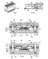
- As a device to achieve the above-stated effect, such one as shown in
FIG. 1 has so far been used. InFIG. 1 ,reference numeral 104 denotes an integrated circuit, IC. The one shown inFIG. 1 is of Dual-In-Line package type but could be of any other type of housing applicable with semiconductor devices.Reference numeral 102 denotes a radiating fin, which is made of metal such as copper, aluminum, or the like, having good heat conductivity, and the radiating fin is provided withfine grooves 102a on the top face thereof to magnify the surface area in contact with the air. Theradiating fin 102 is attached to the top face of theIC 104, a semiconductor device, by means of adhesive, or nuts and bolts. The heat generated by the IC 104 is thus conducted to the radiatingfin 102 for cooling. - The method to attach the
radiating fin 102 directly to theIC 104 appears to be effective upon initial consideration, but it involves various problems in reality. - Firstly, the direction of the
grooves 102a to magnify the surface area of theradiating fin 102 must be in the direction of the air flow. By this arrangement to improve the radiation effect, the direction of theIC 104 to be mounted on the printed circuit board is restricted to be in one direction. As a result, the wiring pattern on the printed circuit board is also subject to restriction. - Secondly, the means used for attaching the
radiating fin 102 toIC 104 involves problems. The means for attaching theradiating fin 102 toIC 104 must endure thermal stress for a long time, so that theradiating fin 102 is held securely attached to theIC 104 even when subject to vibration or shock. However, said means must be adapted such that, under all possible thermal conditions, the semiconductor device does not experience excessive contact pressure resulting from the attaching means. - To achieve this,
US 4,621,304 to Oogaki et al. proposes an adapted construction of a heat sink as indicated in presentFIG. 2 to adjust the height (b). - As indicated in
FIG. 2 , first andsecond heat sink 202, 222 are provided. The second heat sink 222 is of cylindrical shape and provided with athread 222a on the periphery thereof and with a slot 222b on the top face thereof so as to be driven by a screwdriver. Thefirst heat sink 202 attached to ashield case 213 is provided with a female thread 202a, so that the threaded heat sink 222 can be engaged therewith. The threaded heat sink 222 is adapted to be threadedly engaged with the female thread 202a of thefirst heat sink 202 from above theshield case 213, to which theheat sink 202 is attached, through a hole 213a. - The threaded heat sink 222 is passed through the hole 213a at the top of the
shield case 213 and threadedly engaged with the threaded portion 202a of theheat sink 202. The heat sink 222 is pressed against anIC 204 mounted on a printedcircuit board 201. In order to make smooth the contact and the heat conduction between the threaded heat sink 222 and anIC 204, a heatconductive rubber 221 with good heat conductivity may be previously attached to the former at its portion which contacts the latter. In such a case, the threaded heat sink 222 contacts with the IC 204 through therubber 221. Thus, any variation in the distance (a) between theelectronic parts 204 and theheat sink 202 can be minutely compensated with ease by turning the threaded heat sink 222. Meanwhile, the heat sink 202 and the threaded heat sink 222 are in threaded contact and therefore the surface of contact between them is magnified, so that the heat conducted from theelectronic parts 204 through therubber 221 to the threaded heat sink 222 is easily conducted to theheat sink 202, and emitted to the ambient air through theshield case 213. As described in the foregoing, no matter how varied the distances between thefirst heat sink 202 and theelectronic parts 204 may be, sufficient pressure of contact and surface of contact for good heat conductivity is always obtained by virtue of the second heat sink 222. - However, the conventional apparatus shown in
FIG. 2 still exhibits some limitations as, for example, a costly manufacturing process, a multitude of specific parts, and unreasonable weight and height in view of the cooling effect achieved. - In the publication "Research Disclosure, vol. 328, February 2001, pp. 238-240,
XP0001103746 - The spring member described in
US 2002/0051341A1 is a flat plate fastened at the outer edges of the plate to a substrate. Between the substrate and the spring member a circuit package and a stack of heatpipe for cooling the circuit board are located. The spring member is equipped with a dome through which a centering pressure is applied between the cooling stack and the circuit package. Disadvantageous is that the alignment of the stack with respect to the circuit board depends not only on the force applied by the dome but on additional mechanical elements which can cause inhomogeneous pressure between the stack and the circuit board. - In
US 6,256,199 B1 a cartridge including a heat pipe is used as a housing to cover a bottom side of a substrate including a plurality of pins. The cartridge is located on the opposite side of the substrate with respect to a spring clip pressing the substrate against the cartridge. The force inserted into the substrate by the spring clip can only be influenced by a connection between the cartridge and the spring clip but not by the cartridge itself. - To overcome the limitations in the related art as described above, and to overcome other limitations that will become apparent upon reading and understanding the following specification, the present invention discloses an improved apparatus for cooling semiconductor devices attached to a printed circuit board.
- The preferred apparatus for cooling semiconductor devices attached to a printed circuit board comprises: a printed circuit board having first and second sides, said first side having a semiconductor device attached thereto, said printed circuit board further comprises a plurality of apertures formed through said first and second sides; a cooling member adjacent said first side of the printed circuit board and being in thermal contact with the semiconductor device; a spring member adjacent said second side of the printed circuit board; and securing members connecting the spring member to the cooling member through said apertures in the printed circuit board such that the spring member providing a spring force forcing the semiconductor device against the cooling member.
- Therefore, a positive cooling effect is achieved regardless of mounting conditions and the position of the semiconductor device on the cooling plate. Further, the manufacturing process is less costly, less parts are needed, and less weight and less height are.
- The invention can be better understood with reference to the following drawings and description. The components in the figures are not necessarily to scale, emphasis instead is being placed upon illustrating the principles of the invention. In the drawings:
-
FIG. 1 is a perspective view of a conventional heat radiator assembly for a semiconductor device; -
FIG. 2 is a perspective view of another conventional heat radiator assembly for a semiconductor device; -
FIG. 3 is a sectional view of an embodiment of the invention showing a printed circuit board sandwiched between a cooling plate and a spring plate, said spring plate providing a spring force directly to a semiconductor device mounted on the printed circuit board; -
FIG. 4 is a sectional view of a comparative example showing another printed circuit board sandwiched between a cooling plate and a spring in connection with a cover plate, said spring plate providing a spring force via the printed circuit board to a semiconductor device mounted on the printed; -
FIG. 5 is a sectional view of a comparative example showing another printed circuit board sandwiched between a cooling plate and a spring plate, said spring plate being connected to the cooling plate by means of integral noses; -
FIG. 6 is a sectional view of a comparative example showing another printed circuit board sandwiched between a cooling plate and a spring plate, said spring plate being connected to the cooling plate by bolts; and -
FIG. 7 is a sectional view of a comparative example showing another printed circuit board sandwiched between a cooling plate and a spring plate, said printed circuit board having two semiconductor devices mounted thereon. - The present invention provides an apparatus for cooling semiconductor devices attached to a printed circuit board. As shown in
FIG. 3 , such printedcircuit board 301 is sandwiched between a cooling member established by acooling plate 302 and a spring member established by aspring plate 303. - The printed
circuit board 301 is a plate of electrically non-conductive material (e. g. resin plate, cermic substrate) comprising at least one structured electrically conductive layer (e g. metallization) for connecting electrical devices such as semiconductor devices. The printedcircuit board 301 has first and second sides and further comprises a plurality ofapertures 305 formed through said first and second sides. The first side of the printedcircuit board 301 comprises a semiconductor device 304 (e. g. power amplifier, voltage regulator, power switch) attached thereto, e. g. by soldering. InFIG. 3 the printedcircuit board 301 comprises afurther aperture 309 arranged such that it is covered by thesemiconductor device 304. - The
cooling plate 302 is adjacent said first side of the printedcircuit board 301 and has first and second sides itself. The second side of thecooling plate 302 has thermal contact with thesemiconductor device 304. In order to further improve the thermal contact, a heat conductive means 308, e. g. a thermal compound, may be applied between thesemiconductor device 304 and thecooling plate 302. Additionally or alternatively electrically insulating means may be provided between thesemiconductor device 304 and thecooling plate 302. For the purpose of having good heat conductivity, thecooling plate 302 is made of metal and may be provided with fine grooves on the first side thereof to magnify the surface area in contact with the air (not shown in the FIGs.). - The
spring plate 303 is made of metal and arranged adjacent said second side of the printedcircuit board 301. It is wave-like embossed such that it comprises adome 307. Thedome 307 is located in thefurther aperture 309 of the printedcircuit board 301 and has a height relative to its ground line that exceeds the heights of all other waves or domes due to embossing so that thedome 307 is in direct contact with thesemiconductor device 304 and exerting force to thesemiconductor device 304 as a result of the spring force provided by thespring plate 303. Thespring plate 303 comprises apertures 306 corresponding to theapertures 305 of the printedcircuit board 301. - In order to connect the
spring plate 303 to thecooling plate 302, securing members are provided which extend through theapertures 305 of the printedcircuit board 301 and the apertures 306 of thespring plate 303. In the apparatus ofFIG. 3 , the securing members arebolts 310 in connection withintegral noses 311 formed in a single piece from thecooling plate 302. Theintegral noses 311 extend partly into theapertures 305 while thebolts 310 extend throught theapertures 305 and 306 intotap holes 312 arranged in theintegral noses 311. As the case may be, acover plate 313 may be arranged adjacent to thespring plate 302 as an outside surface opposite to the outside surface established by thecooling plate 302. - The apparatus shown in
FIG. 3 can be easily mounted. Starting with thecooling plate 302 as a base plate, the printedcircuit board 301 with thesemiconductor device 304 mounted thereon is arranged on the base plate with thesemiconductor device 304 face down. It is apparent from the drawings, that the height of thesemiconductor device 304 exceeds all other elements arranged on this side of the printedcircuit board 301. The third and last step is just to screw thebolts 310 into the tap holes 312. In the apparatus ofFIG. 3 , the spring force provided by thespring plate 303 depends essentially on the material used, its structure, its thickness, and the size of thedome 307. - As illustrated above, the
spring plate 303 provides a spring force forcing thesemiconductor device 304 against the coolingplate 302 and, thus, providing an excellent thermal contact between thesemiconductor device 304 and thecooling plate 302. Thecooling plate 302 has a lower heat transfer resistance to the air due to a larger surface in contact with the air. - In the comparative example shown in
FIG. 4 , again a printedcircuit board 401 is sandwiched between a coolingplate 402 and aspring plate 403. - Like the one illustrated in
FIG. 3 , the printedcircuit board 401 is a plate of electrically non-conductive material comprising at least one structured electrically conductive layer. The printedcircuit board 401 has first and second sides and comprises a plurality ofapertures 405 formed through said first and second sides. On the first side of the printed circuit board 401 asemiconductor device 404 is arranged. - The
cooling plate 402 made of heat conducting material is adjacent said first side of the printedcircuit board 401 and has first and second sides itself. The second side of thecooling plate 402 has direct thermal contact with thesemiconductor device 404, i. e. no conductive means as mentioned with reference toFIG. 3 is used. - The
spring plate 403 is arranged adjacent said second side of the printedcircuit board 402 and may be wave-like embossed such that it comprises at least onedome 407. Thedome 407 is preferably located in that area of the printedcircuit board 401 where on the other side thesemiconductor device 404 is attached, and is preferably higher than all other waves or domes of thespring plate 403. Thus, thedome 407 forces thesemiconductor device 404 against the coolingplate 402 by means of the printedcircuit board 401. Thespring plate 403 comprisesapertures 406 corresponding to theapertures 405 of the printedcircuit board 401, and has on its outer side a cover member established by acover plate 413 attached thereto. - In order to connect the
cover plate 413 to thespring plate 403 and both to thecooling plate 402,bolts 410 serving as securing members are provided which extend throughapertures 414 in thecover plate 413, spacer leeves 423, theapertures 405 of the printedcircuit board 401, and theapertures 406 of thespring plate 403 and are screwed intotap holes 412 arranged inintegral noses 411 formed in a single piece from thecooling plate 402. - As already mentioned above, the height of the
semiconductor device 404 exceeds all other elements arranged on this side of the printedcircuit board 401. - In the comparative example shown in
FIG. 5 , a printedcircuit board 501 is sandwiched between a coolingplate 502 and aspring plate 503. The printedcircuit board 501, thecooling plate 502, and thespring plate 503 are like those illustrated inFIGs. 3 and 4 . - The printed
circuit board 501 has first and second sides and comprises a plurality ofapertures 505 formed through said first and second sides. On the first side of the printed circuit board 501 asemiconductor device 504 is arranged. - The
cooling plate 502 is adjacent said first side of the printedcircuit board 501 and has first and second sides itself. The second side of thecooling plate 502 has thermal contact with thesemiconductor device 504, said thermal contact is improved by heat conductive means 508, e. g. a thermal compound applied between thesemiconductor device 504 and thecooling plate 502. - The
spring plate 503 is arranged adjacent said second side of the printedcircuit board 502 and is wave-like embossed such that it comprises adome 507. Thedome 507 is preferably located in that area of the printedcircuit board 501 where on the other side thesemiconductor device 504 is attached and is preferably higher than all other waves or domes of thespring plate 503. Thus, thedome 507 forces thesemiconductor device 504 against the coolingplate 502 by exerting force to the printedcircuit board 501 which exerts force to thesemiconductor device 504. Thespring plate 503 comprisesapertures 506 corresponding to theapertures 505 of the printedcircuit board 501. - In order to connect the
spring plate 503 to thecooling plate 502,bolts 510 serving as securing means are provided which extend through theapertures 505 of the printedcircuit board 501, and theapertures 506 of thespring plate 503 and are screwed intotap holes 512 arranged inintegral noses 511 formed in a single piece from thecooling plate 502. The height of thesemiconductor device 504 exceeds all other elements arranged on this side of the printedcircuit board 501. - The comparative example of
FIG. 6 is similar to the apparatus shown inFIG. 5 , wherein, again, a printedcircuit board 601 comprising asemiconductor device 604 is sandwiched between a coolingplate 602 and aspring plate 603. However, thecooling plate 602 comprises no integral noses as thecooling plate 502 ofFIG. 5 . Instead, tapholes 612 corresponding to apertures 605 in the printedcircuit board 601 andapertures 606 in thespring plate 603 are inserted into thecooling plate 602.Bolts 610 extending through theapertures 605 and 606 are screwed into the tap holes 611. Since the cooling plate comprises no noses which would provide counter print to thespring plate 603 as inFIGs. 3-5 , the torque provided by thebolts 610 controls the spring force forcing thesemiconductor device 604 against the coolingplate 602. This means that by screwing thebolts 610 more or less into the tap holes 611, the spring force pressing thesemiconductor device 604 against the coolingplate 602 can easily be adjusted. In the apparatus ofFIG. 6 , as well as in the apparatus ofFIG. 5 , therespective spring plates - The comparative example of
FIG. 7 is similar to the apparatus shown inFIG. 5 , wherein, however, a printedcircuit board 701 having twosemiconductor devices plate 702 and aspring plate 703. - The printed
circuit board 701 has first and second sides and comprises a plurality ofapertures 705 formed through said first and second sides. On the first side of the printedcircuit board 701 the twosemiconductor devices - The
cooling plate 702 is adjacent said first side of the printedcircuit board 701 and has first and second sides itself. The second side of thecooling plate 702 has thermal contact with thesemiconductor devices - The
spring plate 703 is arranged adjacent said second side of the printedcircuit board 702 and is wave-like embossed such that it comprises at least twodomes domes circuit board 701 where on the other side thesemiconductor devices domes spring plate 703. Thus, thedomes semiconductor devices plate 702 by exerting force to the printedcircuit board 701 which exerts force to thesemiconductor devices spring plate 703 comprisesapertures 706 corresponding to theapertures 705 of the printedcircuit board 701. - In order to connect the
spring plate 703 to thecooling plate 702,bolts 710 serving as securing members are provided which extend through theapertures 705 of the printedcircuit board 701, and theapertures 706 of thespring plate 703 and are screwed into tap holes 712 arranged inintegral noses 711 formed in a single piece from thecooling plate 702. Thesemiconductor devices circuit board 701. - It will be apparent to those skilled in the art that various changes and modifications of the embodiment of the invention can be made which achieve some of the advantages of the invention. It will be obvious to those reasonably skilled in the art that other components performing the same functions may be suitably substituted. For example, with all embodiments comprising threaded blind holes as tap holes alternatively threaded contact holes may be used and vice versa. The spring plate may be made of rubber or plastic instead of metal. The semiconductor devices may be integrated circuits or discrete devices in all available and possible packages, e. g. Dual-In-Line (DIL) packages or power packages, preferably PowerS036.
Claims (14)
- An apparatus for cooling semiconductor devices (304) attached to a printed circuit board (301), said apparatus comprising:a printed circuit board (301) having first and second sides, said first side having a semiconductor device (304) attached thereto, said printed circuit board (301) further comprising a plurality of apertures (305) formed through said first and second sides;a cooling member (302) adjacent said first side of the printed circuit board (301) and being in thermal contact with the semiconductor device (304);a spring member (303) adjacent said second side of the printed circuit board (301); andsecuring members (310, 311) connecting the spring member (303) to the cooling member (302) through said apertures (305) in the printed circuit board (301) such that the spring member (303) provides a spring force forcing the semiconductor device (304) against the cooling member (302),
characterized in thatthe spring member (303) comprises a dome (307); and the printed circuit board (301) comprises a further aperture (309); said dome (307) located in said further aperture (309) being in contact with the semiconductor device (304). - The apparatus of claim 1, wherein the spring member (303) has first and second sides and comprises a plurality of apertures (306) formed through said first and second sides; and
wherein the securing members (310, 311) extends through said apertures (306) in the spring member (303). - The apparatus of claim 2, wherein said first side of the spring member (303) is adjacent to the second side of the printed circuit board (301); and
wherein said apparatus further comprises a cover member (313) adjacent said second side of the spring member (303); said cover member (313) being connected to the spring member (303). - The apparatus of one of the preceding claims, wherein the securing members (310, 311) are bolts (310).
- The apparatus of claim 4, wherein the cooling member (302) comprises tap holes (312) into which the bolts (310) are screwed.
- The apparatus of claim 5, wherein the bolts (310) are screwed with a certain torque and said torque is adjustable in order to adjust the spring force provided by the spring member (303).
- The apparatus of one of the preceding claims, wherein the spring force provided by the spring member (303) is adjustable by the dome size.
- The apparatus of one of the preceding claims, wherein the securing members (310, 311) are integral noses (311) formed in a single piece from the cooling member (302).
- The apparatus of claim 8, wherein the spring member (303) is secured to the integral noses (311) by a threaded connection.
- The apparatus of one of the preceding claims, wherein a thermal conductive layer (308) is arranged between the semiconductor device (304) and the cooling member (302).
- The apparatus of one of the preceding claims, wherein the spring member (303) is wave-like embossed.
- The apparatus of one of the preceding claims, wherein the spring member (303) is a spring plate.
- The apparatus of one of the preceding claims, wherein the cooling member (302) is a cooling plate.
- The apparatus of one of the preceding claims, wherein the cover member (313) is a cover plate.
Priority Applications (4)
| Application Number | Priority Date | Filing Date | Title |
|---|---|---|---|
| AT03018046T ATE388487T1 (en) | 2003-08-07 | 2003-08-07 | DEVICE FOR COOLING SEMICONDUCTOR COMPONENTS ON CIRCUIT BOARDS |
| EP03018046A EP1508916B1 (en) | 2003-08-07 | 2003-08-07 | Apparatus for cooling semiconductor devices attached to a printed circuit board |
| DE60319523T DE60319523T2 (en) | 2003-08-07 | 2003-08-07 | Device for cooling semiconductor components on printed circuit boards |
| US10/914,624 US7187553B2 (en) | 2003-08-07 | 2004-08-09 | Apparatus for cooling semiconductor devices attached to a printed circuit board |
Applications Claiming Priority (1)
| Application Number | Priority Date | Filing Date | Title |
|---|---|---|---|
| EP03018046A EP1508916B1 (en) | 2003-08-07 | 2003-08-07 | Apparatus for cooling semiconductor devices attached to a printed circuit board |
Publications (2)
| Publication Number | Publication Date |
|---|---|
| EP1508916A1 EP1508916A1 (en) | 2005-02-23 |
| EP1508916B1 true EP1508916B1 (en) | 2008-03-05 |
Family
ID=34042843
Family Applications (1)
| Application Number | Title | Priority Date | Filing Date |
|---|---|---|---|
| EP03018046A Expired - Lifetime EP1508916B1 (en) | 2003-08-07 | 2003-08-07 | Apparatus for cooling semiconductor devices attached to a printed circuit board |
Country Status (4)
| Country | Link |
|---|---|
| US (1) | US7187553B2 (en) |
| EP (1) | EP1508916B1 (en) |
| AT (1) | ATE388487T1 (en) |
| DE (1) | DE60319523T2 (en) |
Families Citing this family (41)
| Publication number | Priority date | Publication date | Assignee | Title |
|---|---|---|---|---|
| US7321492B2 (en) * | 2005-02-15 | 2008-01-22 | Inventec Corporation | Heat sink module for an electronic device |
| JP2006245356A (en) * | 2005-03-04 | 2006-09-14 | Hitachi Ltd | Cooling apparatus of electronic device |
| US7515418B2 (en) | 2005-09-26 | 2009-04-07 | Curtiss-Wright Controls, Inc. | Adjustable height liquid cooler in liquid flow through plate |
| US7583504B2 (en) * | 2005-11-11 | 2009-09-01 | Telefonaktiebolaget L M Ericsson (Publ) | Cooling assembly |
| US7995344B2 (en) * | 2007-01-09 | 2011-08-09 | Lockheed Martin Corporation | High performance large tolerance heat sink |
| TW200834285A (en) * | 2007-02-02 | 2008-08-16 | Compal Electronics Inc | Fastening structure for reducing surface temperature of housing |
| JP4400662B2 (en) * | 2007-09-12 | 2010-01-20 | 株式会社デンソー | Electronic circuit component mounting structure |
| JP5324773B2 (en) * | 2007-11-06 | 2013-10-23 | インターナショナル・ビジネス・マシーンズ・コーポレーション | Circuit module and manufacturing method thereof |
| AT507352B1 (en) * | 2008-10-01 | 2013-04-15 | Siemens Ag | COOLING ARRANGEMENT |
| JP5402200B2 (en) * | 2009-04-20 | 2014-01-29 | 株式会社リコー | Heat transfer mechanism and information equipment |
| US7957148B1 (en) * | 2009-12-08 | 2011-06-07 | International Business Machines Corporation | Low profile computer processor retention device |
| US20110162828A1 (en) * | 2010-01-06 | 2011-07-07 | Graham Charles Kirk | Thermal plug for use with a heat sink and method of assembling same |
| BR112012021430A2 (en) * | 2010-02-25 | 2020-07-14 | Thomson Licensing | miniature multi-layer radiant radiant cooling case with hidden quick release fasteners |
| US8451600B1 (en) * | 2010-03-04 | 2013-05-28 | Amazon Technologies, Inc. | Heat spreading chassis for rack-mounted computer system |
| US9220185B2 (en) | 2010-05-19 | 2015-12-22 | Thomson Licensing | Set-top box having dissipating thermal loads |
| WO2011155317A1 (en) * | 2010-06-09 | 2011-12-15 | シャープ株式会社 | Heat dissipation structure for electronic device |
| US9209107B2 (en) * | 2010-06-14 | 2015-12-08 | Sharp Kabushiki Kaisha | Electronic device, display device, and television receiver |
| US20130088836A1 (en) * | 2010-06-18 | 2013-04-11 | Tatsuro Kuroda | Heat dissipation structure for electronic device |
| US20130107463A1 (en) * | 2010-07-14 | 2013-05-02 | Sharp Kabushiki Kaisha | Electronic device and display device |
| JP5510432B2 (en) | 2011-02-28 | 2014-06-04 | 株式会社豊田自動織機 | Semiconductor device |
| US9392317B2 (en) | 2011-03-09 | 2016-07-12 | Thomson Licensing | Set top box or server having snap-in heat sink and smart card reader |
| JP5792386B2 (en) | 2011-07-14 | 2015-10-14 | トムソン ライセンシングThomson Licensing | Set-top box with snap-in heat sink and smart card reader with heat sink retention fastener |
| JP5644706B2 (en) * | 2011-07-19 | 2014-12-24 | 株式会社豊田自動織機 | Electronic component fixing structure for electric compressor |
| US8541875B2 (en) * | 2011-09-30 | 2013-09-24 | Alliance For Sustainable Energy, Llc | Integrated three-dimensional module heat exchanger for power electronics cooling |
| TWI504852B (en) * | 2012-09-07 | 2015-10-21 | Compal Electronics Inc | Thermal dissipating module |
| US9049811B2 (en) * | 2012-11-29 | 2015-06-02 | Bose Corporation | Circuit cooling |
| JP5751273B2 (en) * | 2013-04-02 | 2015-07-22 | トヨタ自動車株式会社 | Semiconductor device |
| US9379039B2 (en) * | 2013-09-04 | 2016-06-28 | Cisco Technology, Inc. | Heat transfer for electronic equipment |
| US10455686B2 (en) * | 2016-08-19 | 2019-10-22 | Panasonic Automotive Systems Company Of America, Division Of Panasonic Corporation Of North America | Clamping spring design to apply clamping force to SMT power amplifier device |
| JP6898162B2 (en) * | 2017-06-23 | 2021-07-07 | 矢崎総業株式会社 | Fixed structure of electronic components |
| US10638647B1 (en) * | 2017-12-30 | 2020-04-28 | Xeleum Lighting | Attaching printed circuit board to heat exchanger |
| JP7000931B2 (en) * | 2018-03-12 | 2022-01-19 | 富士通株式会社 | Substrate with cooling mechanism |
| WO2019204686A1 (en) * | 2018-04-19 | 2019-10-24 | The Research Foundation For The State University Of New York | Solderless circuit connector |
| WO2019215805A1 (en) * | 2018-05-08 | 2019-11-14 | 三菱電機株式会社 | Fastening structure and power conversion device using fastening structure |
| JP7193730B2 (en) * | 2019-03-26 | 2022-12-21 | 三菱電機株式会社 | semiconductor equipment |
| DE102019205411A1 (en) | 2019-04-15 | 2020-10-15 | Volkswagen Aktiengesellschaft | Semiconductor device |
| US11495519B2 (en) | 2019-06-07 | 2022-11-08 | Dana Canada Corporation | Apparatus for thermal management of electronic components |
| DE102020212652A1 (en) * | 2020-10-07 | 2022-04-07 | Vitesco Technologies GmbH | Semiconductor assembly and method of manufacturing a semiconductor assembly |
| US11576282B2 (en) * | 2021-06-25 | 2023-02-07 | Intel Corporation | Cold plate attachment with stabilizing arm |
| DE102021129117A1 (en) * | 2021-11-09 | 2023-05-11 | Rolls-Royce Deutschland Ltd & Co Kg | circuit board arrangement |
| SE2151443A1 (en) | 2021-11-26 | 2023-05-27 | Wivid Ab | A printed circuit board with improved cooling properties and method for manufacture thereof |
Family Cites Families (13)
| Publication number | Priority date | Publication date | Assignee | Title |
|---|---|---|---|---|
| EP0130279B1 (en) | 1983-03-25 | 1989-03-08 | Mitsubishi Denki Kabushiki Kaisha | Heat radiator assembly for cooling electronic parts |
| FR2679729B1 (en) * | 1991-07-23 | 1994-04-29 | Alcatel Telspace | HEATSINK. |
| US6046905A (en) * | 1996-09-30 | 2000-04-04 | Intel Corporation | Dual spring clip attachment mechanism for controlled pressure interface thermal solution on processor cartridges |
| US5883782A (en) * | 1997-03-05 | 1999-03-16 | Intel Corporation | Apparatus for attaching a heat sink to a PCB mounted semiconductor package |
| US5883783A (en) * | 1997-07-15 | 1999-03-16 | Intel Corporation | GT clip design for an electronic packaging assembly |
| US5920120A (en) * | 1997-12-19 | 1999-07-06 | Intel Corporation | Assembly for dissipatating heat from a semiconductor chip wherein a stress on the semiconductor chip due to a thermally conductive member is partially relieved |
| US6154365A (en) * | 1999-02-26 | 2000-11-28 | Intel Corporation | Spring fixture that attaches a heat sink to a substrate for multiple cycle assembly/disassembly |
| US6256199B1 (en) * | 1999-10-01 | 2001-07-03 | Intel Corporation | Integrated circuit cartridge and method of fabricating the same |
| JP3602771B2 (en) * | 2000-05-12 | 2004-12-15 | 富士通株式会社 | Portable electronic devices |
| US6469893B1 (en) * | 2000-09-29 | 2002-10-22 | Intel Corporation | Direct heatpipe attachment to die using center point loading |
| TW560643U (en) * | 2002-01-30 | 2003-11-01 | Hon Hai Prec Ind Co Ltd | Backplate of heat sink |
| DE60209423T2 (en) * | 2002-11-08 | 2006-08-10 | Agilent Technologies Inc., A Delaware Corp., Palo Alto | Microchip cooling on circuit board |
| US6885557B2 (en) * | 2003-04-24 | 2005-04-26 | Intel Corporaiton | Heatsink assembly |
-
2003
- 2003-08-07 DE DE60319523T patent/DE60319523T2/en not_active Expired - Lifetime
- 2003-08-07 AT AT03018046T patent/ATE388487T1/en not_active IP Right Cessation
- 2003-08-07 EP EP03018046A patent/EP1508916B1/en not_active Expired - Lifetime
-
2004
- 2004-08-09 US US10/914,624 patent/US7187553B2/en active Active
Also Published As
| Publication number | Publication date |
|---|---|
| DE60319523D1 (en) | 2008-04-17 |
| ATE388487T1 (en) | 2008-03-15 |
| EP1508916A1 (en) | 2005-02-23 |
| DE60319523T2 (en) | 2009-03-26 |
| US20050128713A1 (en) | 2005-06-16 |
| US7187553B2 (en) | 2007-03-06 |
Similar Documents
| Publication | Publication Date | Title |
|---|---|---|
| EP1508916B1 (en) | Apparatus for cooling semiconductor devices attached to a printed circuit board | |
| US5307236A (en) | Heatsink for contact with multiple electronic components mounted on a circuit board | |
| US5787576A (en) | Method for dissipating heat from an integrated circuit | |
| US20200221610A1 (en) | Mechanically flexible cold plates for low power components | |
| EP0625871B1 (en) | Electronic component heat sink attachment using a canted coil spring | |
| EP0130279B1 (en) | Heat radiator assembly for cooling electronic parts | |
| JP3294785B2 (en) | Heat dissipation structure of circuit element | |
| JP2002217343A (en) | Electronic device | |
| US6603665B1 (en) | Heat dissipating assembly with thermal plates | |
| US20060061969A1 (en) | Circuit arrangement for cooling of surface mounted semi-conductors | |
| US6101094A (en) | Printed circuit board with integrated cooling mechanism | |
| US20070133177A1 (en) | Flexing chip heatsink | |
| WO2009110045A1 (en) | Structure for attaching component having heating body mounted thereon | |
| US9807905B2 (en) | Adapter cooling apparatus and method for modular computing devices | |
| JP4643703B2 (en) | Semiconductor device fixture and mounting structure thereof | |
| JPH09283886A (en) | Substrate mounting method, mounting substrate structure and electronic apparatus using mounting substrate structure | |
| CN115294887A (en) | Display module and display device | |
| JPH10107189A (en) | Heat-dissipating device | |
| CN113225934A (en) | Force calculating board and manufacturing method thereof | |
| CN217689993U (en) | Power supply device and computing equipment with same | |
| US6921273B2 (en) | Electric connection arrangement for electronic devices | |
| CN220121226U (en) | CPU heat abstractor | |
| JP4961215B2 (en) | Power device device | |
| CN116321991A (en) | Power element assembling structure | |
| US8050057B2 (en) | Mounting structure for an electronic element |
Legal Events
| Date | Code | Title | Description |
|---|---|---|---|
| PUAI | Public reference made under article 153(3) epc to a published international application that has entered the european phase |
Free format text: ORIGINAL CODE: 0009012 |
|
| 17P | Request for examination filed |
Effective date: 20041013 |
|
| AK | Designated contracting states |
Kind code of ref document: A1 Designated state(s): AT BE BG CH CY CZ DE DK EE ES FI FR GB GR HU IE IT LI LU MC NL PT RO SE SI SK TR |
|
| AX | Request for extension of the european patent |
Extension state: AL LT LV MK |
|
| AKX | Designation fees paid |
Designated state(s): AT BE BG CH CY CZ DE DK EE ES FI FR GB GR HU IE IT LI LU MC NL PT RO SE SI SK TR |
|
| 17Q | First examination report despatched |
Effective date: 20061107 |
|
| GRAP | Despatch of communication of intention to grant a patent |
Free format text: ORIGINAL CODE: EPIDOSNIGR1 |
|
| GRAS | Grant fee paid |
Free format text: ORIGINAL CODE: EPIDOSNIGR3 |
|
| GRAA | (expected) grant |
Free format text: ORIGINAL CODE: 0009210 |
|
| AK | Designated contracting states |
Kind code of ref document: B1 Designated state(s): AT BE BG CH CY CZ DE DK EE ES FI FR GB GR HU IE IT LI LU MC NL PT RO SE SI SK TR |
|
| REG | Reference to a national code |
Ref country code: GB Ref legal event code: FG4D |
|
| REG | Reference to a national code |
Ref country code: CH Ref legal event code: EP |
|
| REG | Reference to a national code |
Ref country code: IE Ref legal event code: FG4D |
|
| REF | Corresponds to: |
Ref document number: 60319523 Country of ref document: DE Date of ref document: 20080417 Kind code of ref document: P |
|
| PG25 | Lapsed in a contracting state [announced via postgrant information from national office to epo] |
Ref country code: FI Free format text: LAPSE BECAUSE OF FAILURE TO SUBMIT A TRANSLATION OF THE DESCRIPTION OR TO PAY THE FEE WITHIN THE PRESCRIBED TIME-LIMIT Effective date: 20080305 Ref country code: ES Free format text: LAPSE BECAUSE OF FAILURE TO SUBMIT A TRANSLATION OF THE DESCRIPTION OR TO PAY THE FEE WITHIN THE PRESCRIBED TIME-LIMIT Effective date: 20080616 |
|
| PG25 | Lapsed in a contracting state [announced via postgrant information from national office to epo] |
Ref country code: AT Free format text: LAPSE BECAUSE OF FAILURE TO SUBMIT A TRANSLATION OF THE DESCRIPTION OR TO PAY THE FEE WITHIN THE PRESCRIBED TIME-LIMIT Effective date: 20080305 |
|
| NLV1 | Nl: lapsed or annulled due to failure to fulfill the requirements of art. 29p and 29m of the patents act | ||
| PG25 | Lapsed in a contracting state [announced via postgrant information from national office to epo] |
Ref country code: SI Free format text: LAPSE BECAUSE OF FAILURE TO SUBMIT A TRANSLATION OF THE DESCRIPTION OR TO PAY THE FEE WITHIN THE PRESCRIBED TIME-LIMIT Effective date: 20080305 Ref country code: BE Free format text: LAPSE BECAUSE OF FAILURE TO SUBMIT A TRANSLATION OF THE DESCRIPTION OR TO PAY THE FEE WITHIN THE PRESCRIBED TIME-LIMIT Effective date: 20080305 |
|
| PG25 | Lapsed in a contracting state [announced via postgrant information from national office to epo] |
Ref country code: SK Free format text: LAPSE BECAUSE OF FAILURE TO SUBMIT A TRANSLATION OF THE DESCRIPTION OR TO PAY THE FEE WITHIN THE PRESCRIBED TIME-LIMIT Effective date: 20080305 Ref country code: PT Free format text: LAPSE BECAUSE OF FAILURE TO SUBMIT A TRANSLATION OF THE DESCRIPTION OR TO PAY THE FEE WITHIN THE PRESCRIBED TIME-LIMIT Effective date: 20080805 Ref country code: SE Free format text: LAPSE BECAUSE OF FAILURE TO SUBMIT A TRANSLATION OF THE DESCRIPTION OR TO PAY THE FEE WITHIN THE PRESCRIBED TIME-LIMIT Effective date: 20080605 Ref country code: CZ Free format text: LAPSE BECAUSE OF FAILURE TO SUBMIT A TRANSLATION OF THE DESCRIPTION OR TO PAY THE FEE WITHIN THE PRESCRIBED TIME-LIMIT Effective date: 20080305 Ref country code: NL Free format text: LAPSE BECAUSE OF FAILURE TO SUBMIT A TRANSLATION OF THE DESCRIPTION OR TO PAY THE FEE WITHIN THE PRESCRIBED TIME-LIMIT Effective date: 20080305 |
|
| PG25 | Lapsed in a contracting state [announced via postgrant information from national office to epo] |
Ref country code: RO Free format text: LAPSE BECAUSE OF FAILURE TO SUBMIT A TRANSLATION OF THE DESCRIPTION OR TO PAY THE FEE WITHIN THE PRESCRIBED TIME-LIMIT Effective date: 20080305 |
|
| ET | Fr: translation filed | ||
| PLBE | No opposition filed within time limit |
Free format text: ORIGINAL CODE: 0009261 |
|
| STAA | Information on the status of an ep patent application or granted ep patent |
Free format text: STATUS: NO OPPOSITION FILED WITHIN TIME LIMIT |
|
| PG25 | Lapsed in a contracting state [announced via postgrant information from national office to epo] |
Ref country code: DK Free format text: LAPSE BECAUSE OF FAILURE TO SUBMIT A TRANSLATION OF THE DESCRIPTION OR TO PAY THE FEE WITHIN THE PRESCRIBED TIME-LIMIT Effective date: 20080305 |
|
| 26N | No opposition filed |
Effective date: 20081208 |
|
| PG25 | Lapsed in a contracting state [announced via postgrant information from national office to epo] |
Ref country code: MC Free format text: LAPSE BECAUSE OF NON-PAYMENT OF DUE FEES Effective date: 20080831 |
|
| REG | Reference to a national code |
Ref country code: CH Ref legal event code: PL |
|
| PG25 | Lapsed in a contracting state [announced via postgrant information from national office to epo] |
Ref country code: BG Free format text: LAPSE BECAUSE OF FAILURE TO SUBMIT A TRANSLATION OF THE DESCRIPTION OR TO PAY THE FEE WITHIN THE PRESCRIBED TIME-LIMIT Effective date: 20080605 Ref country code: EE Free format text: LAPSE BECAUSE OF FAILURE TO SUBMIT A TRANSLATION OF THE DESCRIPTION OR TO PAY THE FEE WITHIN THE PRESCRIBED TIME-LIMIT Effective date: 20080305 |
|
| PG25 | Lapsed in a contracting state [announced via postgrant information from national office to epo] |
Ref country code: CH Free format text: LAPSE BECAUSE OF NON-PAYMENT OF DUE FEES Effective date: 20080831 Ref country code: LI Free format text: LAPSE BECAUSE OF NON-PAYMENT OF DUE FEES Effective date: 20080831 |
|
| PG25 | Lapsed in a contracting state [announced via postgrant information from national office to epo] |
Ref country code: IE Free format text: LAPSE BECAUSE OF NON-PAYMENT OF DUE FEES Effective date: 20080807 |
|
| PG25 | Lapsed in a contracting state [announced via postgrant information from national office to epo] |
Ref country code: CY Free format text: LAPSE BECAUSE OF FAILURE TO SUBMIT A TRANSLATION OF THE DESCRIPTION OR TO PAY THE FEE WITHIN THE PRESCRIBED TIME-LIMIT Effective date: 20080305 |
|
| PG25 | Lapsed in a contracting state [announced via postgrant information from national office to epo] |
Ref country code: LU Free format text: LAPSE BECAUSE OF NON-PAYMENT OF DUE FEES Effective date: 20080807 Ref country code: HU Free format text: LAPSE BECAUSE OF FAILURE TO SUBMIT A TRANSLATION OF THE DESCRIPTION OR TO PAY THE FEE WITHIN THE PRESCRIBED TIME-LIMIT Effective date: 20080906 |
|
| PG25 | Lapsed in a contracting state [announced via postgrant information from national office to epo] |
Ref country code: TR Free format text: LAPSE BECAUSE OF FAILURE TO SUBMIT A TRANSLATION OF THE DESCRIPTION OR TO PAY THE FEE WITHIN THE PRESCRIBED TIME-LIMIT Effective date: 20080305 |
|
| PG25 | Lapsed in a contracting state [announced via postgrant information from national office to epo] |
Ref country code: GR Free format text: LAPSE BECAUSE OF FAILURE TO SUBMIT A TRANSLATION OF THE DESCRIPTION OR TO PAY THE FEE WITHIN THE PRESCRIBED TIME-LIMIT Effective date: 20080606 |
|
| REG | Reference to a national code |
Ref country code: FR Ref legal event code: PLFP Year of fee payment: 14 |
|
| REG | Reference to a national code |
Ref country code: FR Ref legal event code: PLFP Year of fee payment: 15 |
|
| REG | Reference to a national code |
Ref country code: FR Ref legal event code: PLFP Year of fee payment: 16 |
|
| PGFP | Annual fee paid to national office [announced via postgrant information from national office to epo] |
Ref country code: NL Payment date: 20180712 Year of fee payment: 16 Ref country code: IT Payment date: 20180719 Year of fee payment: 16 |
|
| PG25 | Lapsed in a contracting state [announced via postgrant information from national office to epo] |
Ref country code: FR Free format text: LAPSE BECAUSE OF NON-PAYMENT OF DUE FEES Effective date: 20190831 |
|
| PG25 | Lapsed in a contracting state [announced via postgrant information from national office to epo] |
Ref country code: IT Free format text: LAPSE BECAUSE OF NON-PAYMENT OF DUE FEES Effective date: 20190807 |
|
| PGFP | Annual fee paid to national office [announced via postgrant information from national office to epo] |
Ref country code: GB Payment date: 20220721 Year of fee payment: 20 Ref country code: DE Payment date: 20220616 Year of fee payment: 20 |
|
| P01 | Opt-out of the competence of the unified patent court (upc) registered |
Effective date: 20230526 |
|
| REG | Reference to a national code |
Ref country code: DE Ref legal event code: R071 Ref document number: 60319523 Country of ref document: DE |
|
| REG | Reference to a national code |
Ref country code: GB Ref legal event code: PE20 Expiry date: 20230806 |
|
| PG25 | Lapsed in a contracting state [announced via postgrant information from national office to epo] |
Ref country code: GB Free format text: LAPSE BECAUSE OF EXPIRATION OF PROTECTION Effective date: 20230806 |