US11495519B2 - Apparatus for thermal management of electronic components - Google Patents
Apparatus for thermal management of electronic components Download PDFInfo
- Publication number
- US11495519B2 US11495519B2 US16/894,257 US202016894257A US11495519B2 US 11495519 B2 US11495519 B2 US 11495519B2 US 202016894257 A US202016894257 A US 202016894257A US 11495519 B2 US11495519 B2 US 11495519B2
- Authority
- US
- United States
- Prior art keywords
- heat
- interface
- electronic device
- area
- heat spreader
- Prior art date
- Legal status (The legal status is an assumption and is not a legal conclusion. Google has not performed a legal analysis and makes no representation as to the accuracy of the status listed.)
- Active, expires
Links
Images


Classifications
-
- F—MECHANICAL ENGINEERING; LIGHTING; HEATING; WEAPONS; BLASTING
- F28—HEAT EXCHANGE IN GENERAL
- F28F—DETAILS OF HEAT-EXCHANGE AND HEAT-TRANSFER APPARATUS, OF GENERAL APPLICATION
- F28F3/00—Plate-like or laminated elements; Assemblies of plate-like or laminated elements
- F28F3/02—Elements or assemblies thereof with means for increasing heat-transfer area, e.g. with fins, with recesses, with corrugations
- F28F3/06—Elements or assemblies thereof with means for increasing heat-transfer area, e.g. with fins, with recesses, with corrugations the means being attachable to the element
-
- H—ELECTRICITY
- H05—ELECTRIC TECHNIQUES NOT OTHERWISE PROVIDED FOR
- H05K—PRINTED CIRCUITS; CASINGS OR CONSTRUCTIONAL DETAILS OF ELECTRIC APPARATUS; MANUFACTURE OF ASSEMBLAGES OF ELECTRICAL COMPONENTS
- H05K7/00—Constructional details common to different types of electric apparatus
- H05K7/20—Modifications to facilitate cooling, ventilating, or heating
- H05K7/2039—Modifications to facilitate cooling, ventilating, or heating characterised by the heat transfer by conduction from the heat generating element to a dissipating body
-
- F—MECHANICAL ENGINEERING; LIGHTING; HEATING; WEAPONS; BLASTING
- F28—HEAT EXCHANGE IN GENERAL
- F28D—HEAT-EXCHANGE APPARATUS, NOT PROVIDED FOR IN ANOTHER SUBCLASS, IN WHICH THE HEAT-EXCHANGE MEDIA DO NOT COME INTO DIRECT CONTACT
- F28D15/00—Heat-exchange apparatus with the intermediate heat-transfer medium in closed tubes passing into or through the conduit walls ; Heat-exchange apparatus employing intermediate heat-transfer medium or bodies
- F28D15/02—Heat-exchange apparatus with the intermediate heat-transfer medium in closed tubes passing into or through the conduit walls ; Heat-exchange apparatus employing intermediate heat-transfer medium or bodies in which the medium condenses and evaporates, e.g. heat pipes
- F28D15/0233—Heat-exchange apparatus with the intermediate heat-transfer medium in closed tubes passing into or through the conduit walls ; Heat-exchange apparatus employing intermediate heat-transfer medium or bodies in which the medium condenses and evaporates, e.g. heat pipes the conduits having a particular shape, e.g. non-circular cross-section, annular
-
- F—MECHANICAL ENGINEERING; LIGHTING; HEATING; WEAPONS; BLASTING
- F28—HEAT EXCHANGE IN GENERAL
- F28F—DETAILS OF HEAT-EXCHANGE AND HEAT-TRANSFER APPARATUS, OF GENERAL APPLICATION
- F28F3/00—Plate-like or laminated elements; Assemblies of plate-like or laminated elements
- F28F3/02—Elements or assemblies thereof with means for increasing heat-transfer area, e.g. with fins, with recesses, with corrugations
-
- H—ELECTRICITY
- H01—ELECTRIC ELEMENTS
- H01L—SEMICONDUCTOR DEVICES NOT COVERED BY CLASS H10
- H01L23/00—Details of semiconductor or other solid state devices
- H01L23/34—Arrangements for cooling, heating, ventilating or temperature compensation ; Temperature sensing arrangements
- H01L23/36—Selection of materials, or shaping, to facilitate cooling or heating, e.g. heatsinks
- H01L23/367—Cooling facilitated by shape of device
-
- H—ELECTRICITY
- H01—ELECTRIC ELEMENTS
- H01L—SEMICONDUCTOR DEVICES NOT COVERED BY CLASS H10
- H01L23/00—Details of semiconductor or other solid state devices
- H01L23/34—Arrangements for cooling, heating, ventilating or temperature compensation ; Temperature sensing arrangements
- H01L23/40—Mountings or securing means for detachable cooling or heating arrangements ; fixed by friction, plugs or springs
-
- H—ELECTRICITY
- H01—ELECTRIC ELEMENTS
- H01L—SEMICONDUCTOR DEVICES NOT COVERED BY CLASS H10
- H01L23/00—Details of semiconductor or other solid state devices
- H01L23/34—Arrangements for cooling, heating, ventilating or temperature compensation ; Temperature sensing arrangements
- H01L23/42—Fillings or auxiliary members in containers or encapsulations selected or arranged to facilitate heating or cooling
- H01L23/427—Cooling by change of state, e.g. use of heat pipes
-
- H—ELECTRICITY
- H05—ELECTRIC TECHNIQUES NOT OTHERWISE PROVIDED FOR
- H05K—PRINTED CIRCUITS; CASINGS OR CONSTRUCTIONAL DETAILS OF ELECTRIC APPARATUS; MANUFACTURE OF ASSEMBLAGES OF ELECTRICAL COMPONENTS
- H05K7/00—Constructional details common to different types of electric apparatus
- H05K7/20—Modifications to facilitate cooling, ventilating, or heating
- H05K7/2029—Modifications to facilitate cooling, ventilating, or heating using a liquid coolant with phase change in electronic enclosures
- H05K7/20336—Heat pipes, e.g. wicks or capillary pumps
-
- H—ELECTRICITY
- H05—ELECTRIC TECHNIQUES NOT OTHERWISE PROVIDED FOR
- H05K—PRINTED CIRCUITS; CASINGS OR CONSTRUCTIONAL DETAILS OF ELECTRIC APPARATUS; MANUFACTURE OF ASSEMBLAGES OF ELECTRICAL COMPONENTS
- H05K7/00—Constructional details common to different types of electric apparatus
- H05K7/20—Modifications to facilitate cooling, ventilating, or heating
- H05K7/2039—Modifications to facilitate cooling, ventilating, or heating characterised by the heat transfer by conduction from the heat generating element to a dissipating body
- H05K7/20436—Inner thermal coupling elements in heat dissipating housings, e.g. protrusions or depressions integrally formed in the housing
- H05K7/20445—Inner thermal coupling elements in heat dissipating housings, e.g. protrusions or depressions integrally formed in the housing the coupling element being an additional piece, e.g. thermal standoff
-
- H—ELECTRICITY
- H05—ELECTRIC TECHNIQUES NOT OTHERWISE PROVIDED FOR
- H05K—PRINTED CIRCUITS; CASINGS OR CONSTRUCTIONAL DETAILS OF ELECTRIC APPARATUS; MANUFACTURE OF ASSEMBLAGES OF ELECTRICAL COMPONENTS
- H05K7/00—Constructional details common to different types of electric apparatus
- H05K7/20—Modifications to facilitate cooling, ventilating, or heating
- H05K7/2089—Modifications to facilitate cooling, ventilating, or heating for power electronics, e.g. for inverters for controlling motor
- H05K7/20936—Liquid coolant with phase change
-
- F—MECHANICAL ENGINEERING; LIGHTING; HEATING; WEAPONS; BLASTING
- F28—HEAT EXCHANGE IN GENERAL
- F28F—DETAILS OF HEAT-EXCHANGE AND HEAT-TRANSFER APPARATUS, OF GENERAL APPLICATION
- F28F13/00—Arrangements for modifying heat-transfer, e.g. increasing, decreasing
- F28F2013/005—Thermal joints
-
- F—MECHANICAL ENGINEERING; LIGHTING; HEATING; WEAPONS; BLASTING
- F28—HEAT EXCHANGE IN GENERAL
- F28F—DETAILS OF HEAT-EXCHANGE AND HEAT-TRANSFER APPARATUS, OF GENERAL APPLICATION
- F28F13/00—Arrangements for modifying heat-transfer, e.g. increasing, decreasing
- F28F2013/005—Thermal joints
- F28F2013/006—Heat conductive materials
-
- F—MECHANICAL ENGINEERING; LIGHTING; HEATING; WEAPONS; BLASTING
- F28—HEAT EXCHANGE IN GENERAL
- F28F—DETAILS OF HEAT-EXCHANGE AND HEAT-TRANSFER APPARATUS, OF GENERAL APPLICATION
- F28F2215/00—Fins
- F28F2215/08—Fins with openings, e.g. louvers
Definitions
- the present disclosure relates to thermal management of heat-generating electronic components, such as computer chips in electronic devices.
- Electronic devices contain heat-generating electronic components such as computer chips mounted on circuit boards. These computer chips may require cooling to avoid reduced performance and damage caused by overheating. For example, where a computer chip is near its maximum operating limit, its MTBF (Mean Time Before Failure) is reduced by 50 percent for every 10° C. increase in temperature, according to “Military Handbook, Reliability Prediction of Electronic Equipment”, MIL-HDBK-2178B. Therefore, relatively moderate temperature increases can significantly reduce chip life.
- MTBF Mel Time Before Failure
- a heat sink can be used to absorb and dissipate heat generated by a computer chip and/or other heat-generating electronic component in an electronic device.
- the heat sink can sometimes be integrated with the case or housing of the electronic device, or it may comprise a separate element such as a heat spreader which is enclosed within the case or housing. Regardless of its specific form, the heat sink is typically made from metal, having a mass and/or area significantly greater than that of the heat-generating electronic component in order to dissipate the heat.
- the heat sinks may include fins or other heat-dissipating elements.
- heat sinks are comprised of metal, they must be electrically insulated from the heat-generating electronic component. Electrical insulation is typically achieved by providing a layer of dielectric, thermally conductive material between the heat-generating electronic component and the heat sink. Such materials are commonly known as “TIM” (Thermal Interface Material). The TIM layer is applied at the interface between an outer surface of the heat-generating electronic component and a surface of an immediately adjacent heat sink or heat spreader.
- TIM Thermal Interface Material
- the TIM layer can enhance thermal conduction between the heat-generating electronic component and the heat sink, by filling gaps between the electronic component and the heat sink, in order to compensate for manufacturing tolerances of the components and the electronic device.
- the TIM layer may also provide protection from shocks and vibrations.
- the TIM layer may have relatively poor thermal properties, at least compared with the heat sink, leading to higher temperatures of the heat-generating electronic component.
- the application of excessively thick TIM layers to compensate for manufacturing tolerances can further impair heat conduction from the heat-generating electronic component to the adjacent heat sink.
- an electronic device comprising: (a) a heat-generating component having a first surface and an opposite second surface; (b) a heat spreader having a first surface and an opposite second surface, wherein the heat spreader has an area which is at least about 4 times greater than an area of the heat generating component, wherein the first surface of the heat spreader is in thermal contact with the first surface of the heat-generating component along a first interface, and wherein the first interface is non-dielectric and defines a first interface area; (c) a heat sink having a first surface and an opposite second surface, wherein the heat sink has a greater mass than the heat spreader and comprises one or more layers of thermally conductive metal or non-metal between the first and second surfaces of the heat sink, wherein the first surface of the heat sink is in thermal contact with the second surface of the heat spreader along a second interface, wherein the second interface defines a second interface area which is greater than the first interface area; and (d) a layer of
- the heat sink has a greater area than the heat spreader, and a greater thickness, mass and area than the heat-generating component.
- the heat-generating component is a heat-generating electronic component, wherein the second surface of the heat-generating component faces toward a circuit board on which the heat-generating component is mounted.
- the first surface of the heat-generating component is flat, and wherein the area of the heat-generating component is substantially the same as the first interface area.
- the area of the heat spreader is about 5-100 times greater than the area of the heat-generating component.
- the first surface of the heat-generating component is in direct contact with the first surface of the heat spreader along said first interface, without any TIM being provided at the first interface.
- a layer of at material with high thermal conductivity and low dielectric strength is provided at the first interface.
- the layer of TIM at the second interface has a thickness from about 0.1 mm to about 0.5 mm.
- the heat spreader comprises a sheet or plate comprising one or more layers of thermally conductive metal or non-metal.
- the thermally conductive metal is aluminum or copper
- the thermally conductive non-metal is graphite
- the heat spreader comprises a vapor chamber or a heat pipe.
- the heat spreader has a thickness of about 50-2,000 micrometers.
- the heat sink comprises at least a portion of a housing of the electronic device.
- the second surface of the heat sink comprises an external surface of the electronic device.
- the second surface of the heat sink is provided with a plurality of cooling fins.
- the first and second interfaces are spaced apart along an axis which is parallel to the first interface.
- the heat spreader comprises a first portion on which the first interface is defined, a second portion on which the second interface is defined, and a connecting portion which extends between and connects the first and second portions, wherein the second portion has an area which is greater than an area of the first portion.
- the first and second portions of the heat spreader are offset relative to one another along an axis which is perpendicular to the first interface, such that they are located in different planes.
- the electronic device further comprises a resilient member which exerts a compressive force to the heat-generating component and the first portion of the heat spreader at the first interface, wherein the compressive force is directed along an axis which is perpendicular to the first interface.
- the resilient member comprises a layer of a resilient dielectric material which is provided between, and in compressive contact with, the second surface of the heat spreader in the first portion thereof, and an adjacent surface of the electronic device.
- FIG. 1 is a schematic illustration of an electronic device according to the prior art
- FIG. 2 is a view of the device of FIG. 1 , with the circuit board removed;
- FIG. 3 is a schematic illustration of an electronic device according to a first embodiment
- FIG. 4 is a view of the electronic device of FIG. 3 , with the circuit board removed;
- FIG. 5 is a plan view of the electronic device of FIG. 3 , with the circuit board removed;
- FIG. 6 is a partly cut-away plan view of an exemplary heat spreader of the electronic device of FIG. 3 ;
- FIG. 7 is a schematic illustration of an electronic device according to a second embodiment.
- FIG. 8 is a partly cut-away perspective view of the heat spreader of the electronic device of FIG. 7 , shown in isolation.
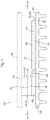
- FIGS. 1 and 2 schematically illustrate a portion of an electronic device 110 according to the prior art.
- Device 110 comprises a heat-generating electronic component 112 such as a computer chip, wherein the heat-generating electronic component 112 has a first surface 114 and a second surface 116 .
- the heat-generating electronic component 112 is mounted on a circuit board 136 , with its second surface 116 in proximity to the circuit board 136 .
- the device 110 further comprises a heat sink 126 having a first surface 128 and a second surface 130 .
- the heat sink 126 is comprised of metal or other thermally conductive material and is adapted to absorb and dissipate heat produced by the heat-generating electronic component 112 .
- the outer surface 130 of heat sink 126 may be provided with cooling fins 144 .
- Heat is conducted across an interface 131 from the first surface 114 of the heat-generating electronic component 112 to the first surface 128 of the heat sink 126 .
- a dielectric layer 134 of TIM is provided at the interface 131 between heat-generating electronic component 112 and heat sink 126 .
- Heat generated by the heat-generating electronic component 112 is conducted through the TIM layer 134 to the heat sink 126 , and is then conducted throughout the heat sink 126 .
- This heat conduction is shown by arrows in FIG. 1 . Although the vertical arrows in FIG. 1 may suggest that the heat flux of the heat-generating electronic component 112 is evenly distributed throughout its entire area, this is not necessarily the case.
- the heat-generating electronic component 112 may include hot spots in which the heat flux is higher than other parts of the component 112 .
- the greater heat flux received from these hot spots may be concentrated in portions of the TIM layer 134 and interface 131 , and these localized heat fluxes do not tend to spread evenly throughout the TIM layer 134 .
- the TIM layer 134 can enhance thermal contact between heat-generating electronic component 112 and heat sink 126 by filling gaps at the interface 131 .
- excessive thickness of the TIM layer 134 can be detrimental to heat transfer, increasing thermal resistance and resulting in higher temperatures of the heat-generating electronic component 112 .
- Q is the amount of heat transferred through TIM layer 134 ;
- the dT through the TIM layer 134 is greater than 17° C.
- the amount of heat transfer (Q) can be increased by reducing the thickness of the TIM layer 134 (L), because Q is inversely proportional to L.
- the thickness of the TIM layer can be reduced to less than about 1 mm, for example from about 0.1-0.5 mm.
- the amount of heat transfer (Q) can be increased by increasing the area (A) of the interface 131 between the heat-generating electronic component 112 and the heat sink 126 , because Q is directly proportional to A.
- the area (A) of interface 131 , and the area of TIM layer 134 are limited to the area of the heat-generating electronic component 112 , which is typically very small.
- the electronic device 10 may comprise any type of computing device, including personal computers and computers integrated into other devices, systems or products, such as an onboard computer of a vehicle control system or entertainment system.
- personal computers include smart phones, tablets, laptops and desktop computers.
- the electronic device 10 includes a heat-generating electronic component 12 having a first surface 14 and an opposite second surface 16 .
- the heat-generating electronic component 12 may comprise one or more computer chips, such as the computer chip for the CPU (central processing unit) or RAM (random access memory) of the electronic device 10 .
- the heat-generating electronic component 12 may comprise a power electronics device which generates significant amounts of heat energy during use, such as a transistor, resistor, capacitor, field effect transistor (FET), isolated gate bipolar transistor (IGBT), power inverter, DC to DC converter, DC to AC converter or other electronic component such as an operational amplifier (op-amp).
- the heat-generating electronic component 12 is shown as being in the shape of a relatively flat rectangular prism, with the first and second surfaces 14 , 16 being the major surfaces of component 12 , having a square or rectangular shape, being opposed to one another, and also being flat and parallel to one another. This is for the purpose of illustration only, and it will be appreciated that the heat-generating electronic component 12 may have other shapes and dimensions.
- the heat-generating electronic component 12 may have an area of roughly 100-225 mm 2 , this being the area of the first or second surface 14 , 16 .
- the first and second surfaces 14 , 16 are square, they may have dimensions from about 10 ⁇ 10 mm 2 to about 15 ⁇ 15 mm 2 , although computer chips having dimensions of 5 ⁇ 5 mm 2 or smaller are known.
- the electronic device 10 includes a printed circuit board 36 through which the heat-generating electronic component 12 is electrically connected to other components (not shown) of the electronic device 10 .
- the heat-generating electronic component 12 may be mounted in any suitable way to the printed circuit board 36 .
- the second surface 16 of heat-generating electronic component 12 may be secured to the circuit board 36 by adhesive or solder (not shown).
- the circuit board 36 is a poor conductor of heat.
- the electronic device 10 further includes a heat spreader 18 and a heat sink 26 .
- the heat spreader 18 which is further described below, has a first surface 20 and an opposite second surface 22 .
- the first surface 20 of the heat spreader 18 is in thermal contact with the first surface 14 of the heat-generating electronic component 12 along a first interface 24 , wherein the first interface 24 defines a first interface area A 1 ( FIG. 5 ).
- the first interface area A 1 is substantially the same as the area of the heat-generating component 12 , and substantially the same as the surface area of the first surface 14 of heat-generating electronic component 12 , through which heat is transferred from the heat-generating electronic component 12 to the heat spreader 18 .
- substantially the same means within ⁇ 15 percent.
- the heat sink 26 has a first surface 28 and a second surface 30 .
- the first surface 28 of the heat sink 26 is in thermal contact with the second surface 22 of the heat spreader 18 along a second interface 32 .
- the second interface 32 defines a second interface area A 2 ( FIG. 5 ) which is greater than the first interface area A 1 , and greater than the area of the heat-generating electronic component 12 .
- the heat sink 26 has greater thickness, mass and area than the heat-generating electronic component 12 , and is adapted to absorb, spread and dissipate the heat produced by the heat-generating electronic component 12 during use of the electronic device 10 .
- the heat sink 26 has mass than the heat spreader 18 , and optionally greater thickness and area than the heat spreader 18 .
- the thickness of heat sink 26 is defined as the thickness of one or more layers of material between first and second surfaces 28 , 30 .
- the drawings show only a portion of the heat sink 26 , however, the area of the heat sink 26 is greater than the area of the second surface 22 of the heat spreader 18 , and greater than the second interface area A 2 .
- the heat sink 26 is comprised of a material having high thermal conductivity, such as a metal or a conductive non-metallic material. Suitable metals include copper and aluminum, including alloys thereof. Suitable non-metallic materials include graphite.
- the heat sink 26 may be located inside the electronic device 10 .
- the heat sink 26 comprises at least a portion of an external housing 40 of the electronic device 10 , which is exposed to the atmosphere along its external surface 42 .
- the second surface 30 of the heat sink 26 may be provided with cooling fins 44 which at least partly define the external surface 42 of the housing 40 . The fins 44 increase the surface area of external surface 42 , to increase heat transfer from heat sink 26 to the atmosphere.
- the first surface 14 of the heat-generating electronic component 12 is in thermal contact with the first surface 20 of the heat spreader 18 , and may be in direct contact with the first surface 20 along the first interface 24 .
- the heat spreader 18 is comprised of a material having high thermal conductivity, such as a metal or a conductive non-metallic material. Suitable metals include copper and aluminum, including alloys thereof. Suitable non-metallic materials include graphite.
- the heat spreader 18 has a flat, sheet or plate-like structure and may be thinner than the heat-generating electronic component 12 , with the first and second surfaces 20 , 22 being opposed to one another and defining the major surfaces of the heat spreader 18 .
- Both surfaces 20 , 22 have the same dimensions, such that both surfaces 20 , 22 and the heat spreader 18 have surface area A 2 .
- Surface area A 2 and the area of heat spreader 18 may be at least about 4 times, for example from about 5-100 times greater, than surface area A 1 and the area of heat-generating electronic component 12 .
- surface area A 2 may be about 4 times greater than surface area A 1 , with the length and width of the heat spreader 18 being approximately double the length and width of the heat-generating electronic component 12 .
- the heat spreader 18 may comprise a simple, flat sheet or plate comprised of metal or a conductive non-metallic material, which relies upon conduction through the plate to spread the heat transferred from the heat-generating electronic component 12 , and which may have a thickness of about 50-2,000 micrometers.
- the heat spreader 18 may comprise a heat pipe or vapor chamber having internal fluid (gas and liquid) flow passages.
- the heat spreader 18 effectively absorbs and spreads the heat produced by heat-generating electronic component 12 during use of the electronic device 10 .
- a layer 34 of dielectric TIM is provided at the second interface 32 , i.e. between and in direct contact with the second surface 22 of heat spreader 18 and the first surface 28 of the heat sink 26 , such that the second interface is dielectric.
- the TIM has a thermal conductivity constant (k) of about 4 W/m 2 K or less.
- the area of the TIM layer 34 is substantially the same as the area A 2 of the second interface 32 and the area of the heat spreader 18 , and may have a thickness from about 0.1 mm to about 0.5 mm.
- the TIM layer 34 at the second interface 32 performs the same electrically insulating and gap filling function as the TIM layer 134 provided at interface 131 in FIGS. 1 and 2 .
- the present embodiment there is typically no need for a layer of a dielectric TIM at the first interface 24 between the heat-generating electronic component 12 and the heat spreader 18 . Rather, high thermal conductivity is desired at the first interface 24 , such that the first interface 24 is non-dielectric. Therefore, the TIM layer at first interface 24 may be completely eliminated.
- a layer of a material with high thermal conductivity and low dielectric strength such as a thermally conductive adhesive, solder or non-dielectric TIM at the first interface 24 , which may be substantially thinner than TIM layer 34 at second interface 32 , to adhere the heat-generating electronic component 12 to the heat spreader 18 , and/or to account for any minor surface irregularities between the heat-generating electronic component 12 to the heat spreader 18 .
- a material with high thermal conductivity and low dielectric strength such as a thermally conductive adhesive, solder or non-dielectric TIM at the first interface 24 , which may be substantially thinner than TIM layer 34 at second interface 32 , to adhere the heat-generating electronic component 12 to the heat spreader 18 , and/or to account for any minor surface irregularities between the heat-generating electronic component 12 to the heat spreader 18 .
- Such materials have a higher thermal conductivity constant than the TIM at the second interface, and typically greater than about 104 W/m 2 K.
- Such a layer of adhesive, solder or TIM at the first interface 24 is sufficiently thin so that it does not significantly increase thermal resistance between the heat-generating electronic component 12 and the heat spreader 18 , and that the TIM layer 34 at the second interface 32 provides the required electrical insulation and fills gaps resulting from manufacturing tolerances.
- TIM layer 34 provided at second interface 32 .
- the area of the TIM layer 34 is significantly greater than the area A of TIM layer 134 in prior art device 110 , because it is not limited by the area of the heat-generating electronic component 12 .
- the amount of heat transfer (Q) is directly proportional to the area of TIM layer 34 which, in electronic device 10 , is substantially the same as area A 2 .
- the inventors have found that a four-fold increase in the area of TIM layer 34 can produce a significant reduction in temperature of the heat-generating electronic component 12 , in some cases being up to about 20° C., particularly where the increase in area of the TIM layer 34 is coupled with a decrease in thickness of the TIM layer 34 .
- the heat from heat-generating electronic component 12 is spread by the heat spreader 18 before passing through a TIM layer of area A 2
- the prior art electronic device 110 passes the heat through a TIM layer of smaller area A 1 , before spreading the heat through heat sink 126 . This is illustrated by arrows in FIG. 3 .
- FIG. 6 is an exemplary heat spreader 18 , in the form of a vapor chamber.
- the heat spreader 18 shown in FIG. 6 may have a construction as disclosed in commonly assigned U.S. patent application Ser. No. 16/047,484, filed on Jul. 27, 2018 and entitled ULTRA THIN HEAT EXCHANGERS FOR THERMAL MANAGEMENT.
- the heat spreader 18 is generally flat and planar and has a thickness ranging from about 200-2,000 micrometers.
- the heat-generating electronic component 12 is received on the heat spreader 18 , and the outline of component 12 is shown as a square in dotted lines in FIG. 6 .
- the heat spreader 18 comprises two metal sheets, a first sheet 46 and a second sheet 48 which are sealingly joined together about their edges, for example by brazing or welding.
- a chamber 38 is enclosed between the sheets 46 , 48 and contains a working fluid such as water.
- the chamber 38 contains a sheet of wick material 50 which may comprise a metal wire mesh.
- the wick material 50 includes a plurality of cutouts which define a plurality of gas flow passages 52 spaced apart across the area of the heat spreader 18 .
- the heat-generating electronic component 12 may be approximately centrally located on the first surface 20 of the heat spreader 18 .
- the gas flow passages 52 may radiate from the approximate center of the heat spreader 18 toward its outer peripheral edges.
- the central area of the heat spreader 18 which is in contact with the heat-generating electronic component 12 and which directly receives heat energy by conduction through first sheet 46 , defines an evaporation zone 54 from which the gas flow passages 52 radiate.
- the working fluid is heated and vaporized in the evaporation zone 54 , thereby absorbing heat energy from the heat-generating electronic component 12 .
- the vaporized working fluid flows outwardly through gas flow passages 52 toward the outer peripheral edges of the heat spreader.
- the vaporized working fluid condenses in these outer areas, releasing heat energy and thereby spreading the heat throughout the area of heat spreader 18 .
- the portions of the heat spreader 18 located outwardly of the heat-generating electronic component 12 therefore define a condensation zone 56 .
- the wick material 50 is hydrophilic and includes a large number of small voids within which capillary forces are generated. The condensed fluid is drawn into these voids and is circulated back to the evaporation zone 54 through the wick material, which defines a plurality of liquid flow passages 58 .
- Electronic device 60 may comprise any of the computing devices described above with reference to device 10 , and includes a number of elements in common with electronic device 10 . These like elements are identified with like reference numerals in the following description.
- Electronic device 60 includes a heat-generating electronic component 12 having a first and second surfaces 14 , 16 , and which may comprise one or more computer chips, as described above.
- Heat-generating electronic component 12 of device 60 is identical to that of device 10 , and therefore the above description of this element with regard to device 10 applies equally to device 60 .
- the electronic device 60 includes a printed circuit board 36 through which the heat-generating electronic component 12 is electrically connected to other components (not shown) of the electronic device 10 .
- the heat-generating electronic component 12 may be secured to the circuit board 36 by adhesive or solder, as described above.
- the electronic device 60 further includes a heat spreader 18 having first and second surfaces 20 , 22 , and a heat sink 26 having first and second surfaces 28 , 30 .
- the heat sink 26 of device 60 may be identical to that of device 10 , and therefore the above description of heat sink 26 of device 10 applies equally to device 60 .
- the first surface 20 of heat spreader 18 is in thermal contact with the first surface 14 of the heat-generating electronic component 12 along a first interface 24 defining a first interface area A 1 .
- the first interface area A 1 is substantially the same as the area of the heat-generating electronic component 12 , and the surface area of the first surface 14 thereof.
- the first surface 28 of the heat sink 26 is in thermal contact with the second surface 22 of the heat spreader 18 along a second interface 32 defining a second interface area A 2 .
- the second interface area A 2 is greater than the first interface area A 1 , and greater than the area of the heat-generating electronic component 12 .
- second interface area A 2 may be at least about 4 times or about 5-100 times greater than interface area A 1 .
- the heat spreader 18 is comprised of one or more layers of a material having high thermal conductivity, such as a metal or a conductive non-metallic material. Suitable metals include copper and aluminum, including alloys thereof, including materials including separate layers of aluminum and copper bonded together. Suitable non-metallic materials include graphite.
- the heat spreader 18 has a flat, plate-like structure with a first surface 20 on which the first interface 24 is defined and an opposite second surface 22 on which the second interface 32 is defined.
- the first and second interfaces 24 , 32 of electronic device 60 are not directly opposed to one another, but rather are spaced apart along an axis L which is parallel to the first interface 24 .
- the arrangement embodied by electronic device 60 is advantageous where the area surrounding heat-generating electronic component 12 is crowded with other components which prevent the insertion of a larger heat spreader 18 directly opposite to the heat-generating electronic component 12 , as in device 10 .
- the arrangement embodied by electronic device 60 permits conduction of heat away from the vicinity of the heat-generating electronic component 12 .
- the heat spreader 18 comprises a first portion 62 on which the first interface 24 is defined, a second portion 64 on which the second interface 32 is defined, and a connecting portion 66 which connects the first and second portions 62 , 64 .
- the second portion 64 has a larger area than the first portion 62 .
- the first and second portions 62 , 64 are both substantially flat and planar, and may be offset relative to one another, such that they lie in different planes.
- the connecting portion 66 extends between the planes defined by first and second portions 62 , 64 , and may be somewhat bendable. The flexibility of connecting portion 66 may be enhanced by making it narrower than one or both of the first and second portions 62 , 64 .
- thermal contact between the first surface 20 of heat spreader 18 and the first surface 14 of heat-generating electronic component 12 may be enhanced by providing a resilient member 68 between the second surface 22 of the heat spreader 18 , in the first portion 62 thereof, and an adjacent surface of electronic device 60 .
- the adjacent surface is the first surface 28 of heat sink 26 .
- the resilient member 68 may be secured to one or both of heat spreader 18 and the adjacent surface by adhesive.
- member 68 allows it to apply a compressive spring force to the heat spreader 18 and the heat-generating electronic component 12 at the first interface 24 , the force being directed along an axis perpendicular to the first interface 24 , to achieve better thermal contact and heat transfer between the heat spreader 18 and the heat-generating electronic component 12 , and to adjust for any manufacturing tolerances.
- the compliance of connecting portion 66 permits some limited movement of the first portion 62 relative to heat-generating electronic component 12 without affecting the thermal contact between second portion 64 and the heat sink 26 .
- the resilient member 68 comprises a layer of resilient dielectric material, such as rubber or synthetic elastomer which is provided between, and in compressive contact with, the second surface 22 of heat spreader 18 in the first portion 62 thereof, and the heat sink 26 of other adjacent surface of electronic device 60 .
- the TIM layer 34 is provided at the second interface 32 , i.e. between the second surface 22 of heat spreader 18 and the first surface 28 of the heat sink 26 , wherein the second surface 22 is provided in the second portion 64 of heat spreader 18 .
- the area of the TIM layer 34 is substantially the same as the area A 2 of the second interface 32 and the area of the second surface 22 of heat spreader 18 .
- Area A 2 is greater than the area A 1 of the first interface 24 , as discussed above.
- the heat spreader 18 may comprise a plate comprised of metal or other thermally conductive material such as graphite, which relies upon conduction through the plate to spread heat from the heat-generating electronic component 12 , to the first portion 62 of heat spreader 18 , through the connecting portion 66 to the second portion 64 .
- the heat spreader 18 may comprise a heat pipe or vapor chamber having internal fluid flow passages.
- FIG. 8 shows an exemplary heat spreader 18 of electronic device 60 , in the form of a vapor chamber.
- the heat spreader 18 of FIG. 8 comprises two metal sheets, a first sheet 46 and a second sheet 48 which are sealingly joined together about their edges, for example by brazing or welding.
- a chamber 38 is enclosed between the sheets 46 , 48 and contains a working fluid such as water.
- the chamber 38 contains a sheet of wick material 50 which may comprise a metal wire mesh and which defines a plurality of liquid flow passages 58 .
- the wick material 50 includes a plurality of cutouts which define a plurality of gas flow passages 52 spaced apart across the area of the heat spreader 18 .
- the evaporation zone 54 of heat spreader 18 of FIG. 8 is provided in the first portion 62 , and the condensation zone 56 is located in the second portion 64 .
- the gas flow passages 52 and the liquid flow passages 58 extend from the evaporation zone 54 to the condensation zone 56 through the connecting portion 66 of heat spreader 18 .
Abstract
Description
Q=k×A×dT/L
-
- k is the thermal conductivity constant of the TIM;
- A is the area of the
TIM layer 134, and the area of theinterface 131 between the heat-generatingelectronic component 112 and theheat sink 126; - dT is the temperature differential between the heat-generating
electronic component 112 and theheat sink 126; and - L is the length of the heat conduction path from the heat-generating
electronic component 112 to theheat sink 126, i.e. the thickness ofTIM layer 134.
Claims (18)
Priority Applications (1)
| Application Number | Priority Date | Filing Date | Title |
|---|---|---|---|
| US16/894,257 US11495519B2 (en) | 2019-06-07 | 2020-06-05 | Apparatus for thermal management of electronic components |
Applications Claiming Priority (2)
| Application Number | Priority Date | Filing Date | Title |
|---|---|---|---|
| US201962858521P | 2019-06-07 | 2019-06-07 | |
| US16/894,257 US11495519B2 (en) | 2019-06-07 | 2020-06-05 | Apparatus for thermal management of electronic components |
Publications (2)
| Publication Number | Publication Date |
|---|---|
| US20200388555A1 US20200388555A1 (en) | 2020-12-10 |
| US11495519B2 true US11495519B2 (en) | 2022-11-08 |
Family
ID=73459973
Family Applications (1)
| Application Number | Title | Priority Date | Filing Date |
|---|---|---|---|
| US16/894,257 Active 2041-03-20 US11495519B2 (en) | 2019-06-07 | 2020-06-05 | Apparatus for thermal management of electronic components |
Country Status (3)
| Country | Link |
|---|---|
| US (1) | US11495519B2 (en) |
| CN (1) | CN112055506A (en) |
| DE (1) | DE102020207150A1 (en) |
Families Citing this family (3)
| Publication number | Priority date | Publication date | Assignee | Title |
|---|---|---|---|---|
| JP2021089994A (en) * | 2019-12-05 | 2021-06-10 | 日立Astemo株式会社 | On-vehicle electronic control device |
| KR102379341B1 (en) * | 2020-02-28 | 2022-03-25 | 엘지전자 주식회사 | Apparatus for heatsink |
| CN113873851B (en) * | 2021-10-13 | 2024-04-09 | 燕山大学 | Radiation heat dissipation equipment |
Citations (26)
| Publication number | Priority date | Publication date | Assignee | Title |
|---|---|---|---|---|
| US6158502A (en) | 1996-11-18 | 2000-12-12 | Novel Concepts, Inc. | Thin planar heat spreader |
| US20030111213A1 (en) * | 2001-12-14 | 2003-06-19 | Chang Je Young | Use of adjusted evaporator section area of heat pipe that is sized to match the surface area of an integrated heat spreader used in CPU packages in mobile computers |
| EP1508916A1 (en) | 2003-08-07 | 2005-02-23 | Harman Becker Automotive Systems GmbH | Apparatus for cooling semiconductor devices attached to a printed circuit board |
| US20050180113A1 (en) | 2004-02-13 | 2005-08-18 | Takashi Shirakami | Heat transfer mechanism, heat dissipation system, and communication apparatus |
| US20100059870A1 (en) | 2008-09-10 | 2010-03-11 | Cyntec Co., Ltd. | Chip package structure |
| US7755894B2 (en) | 2006-03-16 | 2010-07-13 | Fu Zhun Precision Industry (Shen Zhen) Co., Ltd. | Heat dissipation device |
| US20100224985A1 (en) * | 2009-03-05 | 2010-09-09 | Mihalis Michael | Chip-Scale Packaging with Protective Heat Spreader |
| US20110067906A1 (en) | 2008-05-16 | 2011-03-24 | Mitsubishi Materials Corporation | Power module substrate, power module, and method for manufacturing power module substrate |
| US20120139093A1 (en) * | 2010-12-01 | 2012-06-07 | Start Paul R | In-situ foam material as integrated heat spreader (ihs) sealant |
| US20140328016A1 (en) * | 2011-10-03 | 2014-11-06 | Invensas Corporation | Stub minimization for multi-die wirebond assemblies with parallel windows |
| US20150195956A1 (en) * | 2014-01-08 | 2015-07-09 | Enphase Energy, Inc. | Double insulated heat spreader |
| US20150301568A1 (en) * | 2014-04-18 | 2015-10-22 | Laird Technologies, Inc. | Thermal Solutions and Methods for Dissipating Heat from Electronic Devices Using the Same Side of an Anisotropic Heat Spreader |
| US20170023306A1 (en) | 2015-07-22 | 2017-01-26 | Compulab Ltd. | Layered heat pipe structure for cooling electronic component |
| US20170083061A1 (en) * | 2015-09-23 | 2017-03-23 | Microsoft Technology Licensing, Llc | Hybrid thermal solution for electronic devices |
| US9640511B2 (en) | 2015-03-25 | 2017-05-02 | Infineon Technologies Ag | Method for producing a circuit carrier arrangement having a carrier which has a surface formed by an aluminum/silicon carbide metal matrix composite material |
| US20170167800A1 (en) * | 2015-12-11 | 2017-06-15 | California Institute Of Technology | Silicon biporous wick for high heat flux heat spreaders |
| US20180027694A1 (en) | 2016-07-21 | 2018-01-25 | Lenovo (Singapore) Pte. Ltd. | Electronic apparatus |
| US9911715B2 (en) | 2013-12-20 | 2018-03-06 | Cyntec Co., Ltd. | Three-dimensional package structure and the method to fabricate thereof |
| US20180114742A1 (en) | 2016-10-20 | 2018-04-26 | Harman Becker Automotive Systems Gmbh | Heat sink fastening system and method |
| US10123454B2 (en) * | 2015-03-30 | 2018-11-06 | Exascaler Inc. | Electronic-device cooling system |
| US20180374716A1 (en) * | 2017-06-21 | 2018-12-27 | International Business Machines Corporation | Adhesive-bonded thermal interface structures |
| US20190033006A1 (en) | 2017-07-28 | 2019-01-31 | Dana Canada Corporation | Ultra Thin Heat Exchangers For Thermal Management |
| US20190074235A1 (en) * | 2017-09-01 | 2019-03-07 | Analog Devices, Inc. | Diamond-based heat spreading substrates for integrated circuit dies |
| US20200022285A1 (en) | 2015-11-19 | 2020-01-16 | Boyd Corporation | Densified foam for thermal insulation in electronic devices |
| WO2020061267A1 (en) | 2017-10-18 | 2020-03-26 | Boyd Corporation | Titanium Thermal Module |
| US20200329551A1 (en) * | 2019-04-10 | 2020-10-15 | Fujitsu Limited | Heat sink fixing member and electronic device |
-
2020
- 2020-06-05 US US16/894,257 patent/US11495519B2/en active Active
- 2020-06-08 CN CN202010512009.6A patent/CN112055506A/en active Pending
- 2020-06-08 DE DE102020207150.0A patent/DE102020207150A1/en active Pending
Patent Citations (26)
| Publication number | Priority date | Publication date | Assignee | Title |
|---|---|---|---|---|
| US6158502A (en) | 1996-11-18 | 2000-12-12 | Novel Concepts, Inc. | Thin planar heat spreader |
| US20030111213A1 (en) * | 2001-12-14 | 2003-06-19 | Chang Je Young | Use of adjusted evaporator section area of heat pipe that is sized to match the surface area of an integrated heat spreader used in CPU packages in mobile computers |
| EP1508916A1 (en) | 2003-08-07 | 2005-02-23 | Harman Becker Automotive Systems GmbH | Apparatus for cooling semiconductor devices attached to a printed circuit board |
| US20050180113A1 (en) | 2004-02-13 | 2005-08-18 | Takashi Shirakami | Heat transfer mechanism, heat dissipation system, and communication apparatus |
| US7755894B2 (en) | 2006-03-16 | 2010-07-13 | Fu Zhun Precision Industry (Shen Zhen) Co., Ltd. | Heat dissipation device |
| US20110067906A1 (en) | 2008-05-16 | 2011-03-24 | Mitsubishi Materials Corporation | Power module substrate, power module, and method for manufacturing power module substrate |
| US20100059870A1 (en) | 2008-09-10 | 2010-03-11 | Cyntec Co., Ltd. | Chip package structure |
| US20100224985A1 (en) * | 2009-03-05 | 2010-09-09 | Mihalis Michael | Chip-Scale Packaging with Protective Heat Spreader |
| US20120139093A1 (en) * | 2010-12-01 | 2012-06-07 | Start Paul R | In-situ foam material as integrated heat spreader (ihs) sealant |
| US20140328016A1 (en) * | 2011-10-03 | 2014-11-06 | Invensas Corporation | Stub minimization for multi-die wirebond assemblies with parallel windows |
| US9911715B2 (en) | 2013-12-20 | 2018-03-06 | Cyntec Co., Ltd. | Three-dimensional package structure and the method to fabricate thereof |
| US20150195956A1 (en) * | 2014-01-08 | 2015-07-09 | Enphase Energy, Inc. | Double insulated heat spreader |
| US20150301568A1 (en) * | 2014-04-18 | 2015-10-22 | Laird Technologies, Inc. | Thermal Solutions and Methods for Dissipating Heat from Electronic Devices Using the Same Side of an Anisotropic Heat Spreader |
| US9640511B2 (en) | 2015-03-25 | 2017-05-02 | Infineon Technologies Ag | Method for producing a circuit carrier arrangement having a carrier which has a surface formed by an aluminum/silicon carbide metal matrix composite material |
| US10123454B2 (en) * | 2015-03-30 | 2018-11-06 | Exascaler Inc. | Electronic-device cooling system |
| US20170023306A1 (en) | 2015-07-22 | 2017-01-26 | Compulab Ltd. | Layered heat pipe structure for cooling electronic component |
| US20170083061A1 (en) * | 2015-09-23 | 2017-03-23 | Microsoft Technology Licensing, Llc | Hybrid thermal solution for electronic devices |
| US20200022285A1 (en) | 2015-11-19 | 2020-01-16 | Boyd Corporation | Densified foam for thermal insulation in electronic devices |
| US20170167800A1 (en) * | 2015-12-11 | 2017-06-15 | California Institute Of Technology | Silicon biporous wick for high heat flux heat spreaders |
| US20180027694A1 (en) | 2016-07-21 | 2018-01-25 | Lenovo (Singapore) Pte. Ltd. | Electronic apparatus |
| US20180114742A1 (en) | 2016-10-20 | 2018-04-26 | Harman Becker Automotive Systems Gmbh | Heat sink fastening system and method |
| US20180374716A1 (en) * | 2017-06-21 | 2018-12-27 | International Business Machines Corporation | Adhesive-bonded thermal interface structures |
| US20190033006A1 (en) | 2017-07-28 | 2019-01-31 | Dana Canada Corporation | Ultra Thin Heat Exchangers For Thermal Management |
| US20190074235A1 (en) * | 2017-09-01 | 2019-03-07 | Analog Devices, Inc. | Diamond-based heat spreading substrates for integrated circuit dies |
| WO2020061267A1 (en) | 2017-10-18 | 2020-03-26 | Boyd Corporation | Titanium Thermal Module |
| US20200329551A1 (en) * | 2019-04-10 | 2020-10-15 | Fujitsu Limited | Heat sink fixing member and electronic device |
Also Published As
| Publication number | Publication date |
|---|---|
| US20200388555A1 (en) | 2020-12-10 |
| DE102020207150A1 (en) | 2020-12-10 |
| CN112055506A (en) | 2020-12-08 |
Similar Documents
| Publication | Publication Date | Title |
|---|---|---|
| US11495519B2 (en) | Apparatus for thermal management of electronic components | |
| US8488325B1 (en) | Memory module having thermal conduits | |
| EP3503701B1 (en) | Heat sink, heat dissipation apparatus, heat dissipation system and communication device | |
| US6639799B2 (en) | Integrated vapor chamber heat sink and spreader and an embedded direct heat pipe attachment | |
| KR100836305B1 (en) | Thermoelectric module | |
| US5933323A (en) | Electronic component lid that provides improved thermal dissipation | |
| US7078109B2 (en) | Heat spreading thermal interface structure | |
| TWI458927B (en) | Heat sink | |
| JP5936313B2 (en) | Electronic component mounting structure | |
| US20120085520A1 (en) | Heat spreader with flexibly supported heat pipe | |
| US20070217162A1 (en) | Heat dissipation device | |
| JP4935220B2 (en) | Power module device | |
| US20110038122A1 (en) | Phase Change Heat Spreader Bonded to Power Module by Energetic Multilayer Foil | |
| US20050088823A1 (en) | Variable density graphite foam heat sink | |
| KR100700936B1 (en) | Cooling apparatus and memory module having the same | |
| US9030823B2 (en) | Heat dissipation system for power module | |
| US6760222B1 (en) | Dissipating heat using a heat conduit | |
| JPH10313184A (en) | Heat-dissipating structure of electronic equipment | |
| WO2014140098A1 (en) | Heat spreader with flat pipe cooling element | |
| JP2006196593A (en) | Semiconductor device and heat sink | |
| KR101044351B1 (en) | Heat cooler | |
| JP5554444B1 (en) | Compound package cooling structure | |
| JP4430451B2 (en) | Semiconductor device heat dissipation device | |
| JP5485450B1 (en) | Heat spreader | |
| JPS60171751A (en) | Heat dissipating construction of ic |
Legal Events
| Date | Code | Title | Description |
|---|---|---|---|
| FEPP | Fee payment procedure |
Free format text: ENTITY STATUS SET TO UNDISCOUNTED (ORIGINAL EVENT CODE: BIG.); ENTITY STATUS OF PATENT OWNER: LARGE ENTITY |
|
| AS | Assignment |
Owner name: DANA CANADA CORPORATION, CANADA Free format text: ASSIGNMENT OF ASSIGNORS INTEREST;ASSIGNOR:VANDERWEES, DOUG;REEL/FRAME:053050/0199 Effective date: 20200609 |
|
| STPP | Information on status: patent application and granting procedure in general |
Free format text: APPLICATION DISPATCHED FROM PREEXAM, NOT YET DOCKETED |
|
| STPP | Information on status: patent application and granting procedure in general |
Free format text: DOCKETED NEW CASE - READY FOR EXAMINATION |
|
| STPP | Information on status: patent application and granting procedure in general |
Free format text: NON FINAL ACTION MAILED |
|
| STPP | Information on status: patent application and granting procedure in general |
Free format text: RESPONSE TO NON-FINAL OFFICE ACTION ENTERED AND FORWARDED TO EXAMINER |
|
| STPP | Information on status: patent application and granting procedure in general |
Free format text: FINAL REJECTION MAILED |
|
| STPP | Information on status: patent application and granting procedure in general |
Free format text: NOTICE OF ALLOWANCE MAILED -- APPLICATION RECEIVED IN OFFICE OF PUBLICATIONS |
|
| STPP | Information on status: patent application and granting procedure in general |
Free format text: PUBLICATIONS -- ISSUE FEE PAYMENT RECEIVED |
|
| STPP | Information on status: patent application and granting procedure in general |
Free format text: PUBLICATIONS -- ISSUE FEE PAYMENT VERIFIED |
|
| STCF | Information on status: patent grant |
Free format text: PATENTED CASE |