EP1507162B1 - Liquid crystal display device - Google Patents
Liquid crystal display device Download PDFInfo
- Publication number
- EP1507162B1 EP1507162B1 EP04022587A EP04022587A EP1507162B1 EP 1507162 B1 EP1507162 B1 EP 1507162B1 EP 04022587 A EP04022587 A EP 04022587A EP 04022587 A EP04022587 A EP 04022587A EP 1507162 B1 EP1507162 B1 EP 1507162B1
- Authority
- EP
- European Patent Office
- Prior art keywords
- liquid crystal
- area
- display area
- dummy
- display
- Prior art date
- Legal status (The legal status is an assumption and is not a legal conclusion. Google has not performed a legal analysis and makes no representation as to the accuracy of the status listed.)
- Expired - Lifetime
Links
Images


Classifications
-
- G—PHYSICS
- G02—OPTICS
- G02F—OPTICAL DEVICES OR ARRANGEMENTS FOR THE CONTROL OF LIGHT BY MODIFICATION OF THE OPTICAL PROPERTIES OF THE MEDIA OF THE ELEMENTS INVOLVED THEREIN; NON-LINEAR OPTICS; FREQUENCY-CHANGING OF LIGHT; OPTICAL LOGIC ELEMENTS; OPTICAL ANALOGUE/DIGITAL CONVERTERS
- G02F1/00—Devices or arrangements for the control of the intensity, colour, phase, polarisation or direction of light arriving from an independent light source, e.g. switching, gating or modulating; Non-linear optics
- G02F1/01—Devices or arrangements for the control of the intensity, colour, phase, polarisation or direction of light arriving from an independent light source, e.g. switching, gating or modulating; Non-linear optics for the control of the intensity, phase, polarisation or colour
- G02F1/13—Devices or arrangements for the control of the intensity, colour, phase, polarisation or direction of light arriving from an independent light source, e.g. switching, gating or modulating; Non-linear optics for the control of the intensity, phase, polarisation or colour based on liquid crystals, e.g. single liquid crystal display cells
- G02F1/133—Constructional arrangements; Operation of liquid crystal cells; Circuit arrangements
- G02F1/1333—Constructional arrangements; Manufacturing methods
- G02F1/1335—Structural association of cells with optical devices, e.g. polarisers or reflectors
- G02F1/133509—Filters, e.g. light shielding masks
- G02F1/133514—Colour filters
-
- G—PHYSICS
- G02—OPTICS
- G02F—OPTICAL DEVICES OR ARRANGEMENTS FOR THE CONTROL OF LIGHT BY MODIFICATION OF THE OPTICAL PROPERTIES OF THE MEDIA OF THE ELEMENTS INVOLVED THEREIN; NON-LINEAR OPTICS; FREQUENCY-CHANGING OF LIGHT; OPTICAL LOGIC ELEMENTS; OPTICAL ANALOGUE/DIGITAL CONVERTERS
- G02F1/00—Devices or arrangements for the control of the intensity, colour, phase, polarisation or direction of light arriving from an independent light source, e.g. switching, gating or modulating; Non-linear optics
- G02F1/01—Devices or arrangements for the control of the intensity, colour, phase, polarisation or direction of light arriving from an independent light source, e.g. switching, gating or modulating; Non-linear optics for the control of the intensity, phase, polarisation or colour
- G02F1/13—Devices or arrangements for the control of the intensity, colour, phase, polarisation or direction of light arriving from an independent light source, e.g. switching, gating or modulating; Non-linear optics for the control of the intensity, phase, polarisation or colour based on liquid crystals, e.g. single liquid crystal display cells
- G02F1/133—Constructional arrangements; Operation of liquid crystal cells; Circuit arrangements
- G02F1/1333—Constructional arrangements; Manufacturing methods
- G02F1/1339—Gaskets; Spacers; Sealing of cells
-
- G—PHYSICS
- G02—OPTICS
- G02F—OPTICAL DEVICES OR ARRANGEMENTS FOR THE CONTROL OF LIGHT BY MODIFICATION OF THE OPTICAL PROPERTIES OF THE MEDIA OF THE ELEMENTS INVOLVED THEREIN; NON-LINEAR OPTICS; FREQUENCY-CHANGING OF LIGHT; OPTICAL LOGIC ELEMENTS; OPTICAL ANALOGUE/DIGITAL CONVERTERS
- G02F1/00—Devices or arrangements for the control of the intensity, colour, phase, polarisation or direction of light arriving from an independent light source, e.g. switching, gating or modulating; Non-linear optics
- G02F1/01—Devices or arrangements for the control of the intensity, colour, phase, polarisation or direction of light arriving from an independent light source, e.g. switching, gating or modulating; Non-linear optics for the control of the intensity, phase, polarisation or colour
- G02F1/13—Devices or arrangements for the control of the intensity, colour, phase, polarisation or direction of light arriving from an independent light source, e.g. switching, gating or modulating; Non-linear optics for the control of the intensity, phase, polarisation or colour based on liquid crystals, e.g. single liquid crystal display cells
- G02F1/133—Constructional arrangements; Operation of liquid crystal cells; Circuit arrangements
- G02F1/1333—Constructional arrangements; Manufacturing methods
- G02F1/1343—Electrodes
- G02F1/134309—Electrodes characterised by their geometrical arrangement
- G02F1/134336—Matrix
-
- G—PHYSICS
- G02—OPTICS
- G02F—OPTICAL DEVICES OR ARRANGEMENTS FOR THE CONTROL OF LIGHT BY MODIFICATION OF THE OPTICAL PROPERTIES OF THE MEDIA OF THE ELEMENTS INVOLVED THEREIN; NON-LINEAR OPTICS; FREQUENCY-CHANGING OF LIGHT; OPTICAL LOGIC ELEMENTS; OPTICAL ANALOGUE/DIGITAL CONVERTERS
- G02F1/00—Devices or arrangements for the control of the intensity, colour, phase, polarisation or direction of light arriving from an independent light source, e.g. switching, gating or modulating; Non-linear optics
- G02F1/01—Devices or arrangements for the control of the intensity, colour, phase, polarisation or direction of light arriving from an independent light source, e.g. switching, gating or modulating; Non-linear optics for the control of the intensity, phase, polarisation or colour
- G02F1/13—Devices or arrangements for the control of the intensity, colour, phase, polarisation or direction of light arriving from an independent light source, e.g. switching, gating or modulating; Non-linear optics for the control of the intensity, phase, polarisation or colour based on liquid crystals, e.g. single liquid crystal display cells
- G02F1/133—Constructional arrangements; Operation of liquid crystal cells; Circuit arrangements
- G02F1/1333—Constructional arrangements; Manufacturing methods
- G02F1/133388—Constructional arrangements; Manufacturing methods with constructional differences between the display region and the peripheral region
-
- G—PHYSICS
- G02—OPTICS
- G02F—OPTICAL DEVICES OR ARRANGEMENTS FOR THE CONTROL OF LIGHT BY MODIFICATION OF THE OPTICAL PROPERTIES OF THE MEDIA OF THE ELEMENTS INVOLVED THEREIN; NON-LINEAR OPTICS; FREQUENCY-CHANGING OF LIGHT; OPTICAL LOGIC ELEMENTS; OPTICAL ANALOGUE/DIGITAL CONVERTERS
- G02F1/00—Devices or arrangements for the control of the intensity, colour, phase, polarisation or direction of light arriving from an independent light source, e.g. switching, gating or modulating; Non-linear optics
- G02F1/01—Devices or arrangements for the control of the intensity, colour, phase, polarisation or direction of light arriving from an independent light source, e.g. switching, gating or modulating; Non-linear optics for the control of the intensity, phase, polarisation or colour
- G02F1/13—Devices or arrangements for the control of the intensity, colour, phase, polarisation or direction of light arriving from an independent light source, e.g. switching, gating or modulating; Non-linear optics for the control of the intensity, phase, polarisation or colour based on liquid crystals, e.g. single liquid crystal display cells
- G02F1/133—Constructional arrangements; Operation of liquid crystal cells; Circuit arrangements
- G02F1/1333—Constructional arrangements; Manufacturing methods
- G02F1/1337—Surface-induced orientation of the liquid crystal molecules, e.g. by alignment layers
-
- G—PHYSICS
- G02—OPTICS
- G02F—OPTICAL DEVICES OR ARRANGEMENTS FOR THE CONTROL OF LIGHT BY MODIFICATION OF THE OPTICAL PROPERTIES OF THE MEDIA OF THE ELEMENTS INVOLVED THEREIN; NON-LINEAR OPTICS; FREQUENCY-CHANGING OF LIGHT; OPTICAL LOGIC ELEMENTS; OPTICAL ANALOGUE/DIGITAL CONVERTERS
- G02F1/00—Devices or arrangements for the control of the intensity, colour, phase, polarisation or direction of light arriving from an independent light source, e.g. switching, gating or modulating; Non-linear optics
- G02F1/01—Devices or arrangements for the control of the intensity, colour, phase, polarisation or direction of light arriving from an independent light source, e.g. switching, gating or modulating; Non-linear optics for the control of the intensity, phase, polarisation or colour
- G02F1/13—Devices or arrangements for the control of the intensity, colour, phase, polarisation or direction of light arriving from an independent light source, e.g. switching, gating or modulating; Non-linear optics for the control of the intensity, phase, polarisation or colour based on liquid crystals, e.g. single liquid crystal display cells
- G02F1/133—Constructional arrangements; Operation of liquid crystal cells; Circuit arrangements
- G02F1/1333—Constructional arrangements; Manufacturing methods
- G02F1/1345—Conductors connecting electrodes to cell terminals
- G02F1/13454—Drivers integrated on the active matrix substrate
-
- G—PHYSICS
- G02—OPTICS
- G02F—OPTICAL DEVICES OR ARRANGEMENTS FOR THE CONTROL OF LIGHT BY MODIFICATION OF THE OPTICAL PROPERTIES OF THE MEDIA OF THE ELEMENTS INVOLVED THEREIN; NON-LINEAR OPTICS; FREQUENCY-CHANGING OF LIGHT; OPTICAL LOGIC ELEMENTS; OPTICAL ANALOGUE/DIGITAL CONVERTERS
- G02F1/00—Devices or arrangements for the control of the intensity, colour, phase, polarisation or direction of light arriving from an independent light source, e.g. switching, gating or modulating; Non-linear optics
- G02F1/01—Devices or arrangements for the control of the intensity, colour, phase, polarisation or direction of light arriving from an independent light source, e.g. switching, gating or modulating; Non-linear optics for the control of the intensity, phase, polarisation or colour
- G02F1/13—Devices or arrangements for the control of the intensity, colour, phase, polarisation or direction of light arriving from an independent light source, e.g. switching, gating or modulating; Non-linear optics for the control of the intensity, phase, polarisation or colour based on liquid crystals, e.g. single liquid crystal display cells
- G02F1/133—Constructional arrangements; Operation of liquid crystal cells; Circuit arrangements
- G02F1/136—Liquid crystal cells structurally associated with a semi-conducting layer or substrate, e.g. cells forming part of an integrated circuit
- G02F1/1362—Active matrix addressed cells
- G02F1/1368—Active matrix addressed cells in which the switching element is a three-electrode device
Description
- The present invention relates to a liquid crystal display device for displaying image or the like.
- The characteristics required for the liquid crystal display device have become stricter in the recent years, and the displayed image quality on such device is required to be of the same level as in the ordinary CRT image. In the liquid crystal display device, the control of the orientation of the employed liquid crystal is a major factor governing the quality of the displayed image, and uniform and optimum orientation in any part of the display unit is an essential requirement. In general, the orientation of the liquid crystal is controlled by an alignment control film provided on the surface of liquid crystal.
- If such alignment control film has a surfacial step, the orientation of the liquid crystal varies at such stepped portion and becomes no longer uniform. However, particularly on the pixel electrode substrate, the alignment control film develops surfacial steps because of the formation of the pixel electrodes, switching elements, wirings etc. on said substrate. Particularly at the end of the display area, the film position becomes extremely low because of the absence of the adjacent pixel electrode, so that the display characteristics become inferior in such end portion of the display area.
- The liquid crystal display device is composed of mutually adhered two substrates bearing electrodes on the internal faces thereof and sandwiching a liquid crystal layer therebetween, and peripheral circuits for driving the liquid crystal device are often provided in the peripheral area of the pixel areas.
- In the mutual adhesion of both substrates, if a
seal area 32 is formed on theperipheral circuits 31 as shown in Fig. 1, there is generated a distribution in the gap of the filledliquid crystal part 33, and an unevenness in color is generated if said distribution exceeds ±0.1 µ. - On the other hand, if the
seal area 32 is provided outside theperipheral circuits 31 as shown in Fig. 2, the chip size becomes inevitably larger, and this will pose a serious problem in a liquid crystal display device requiring a very small cell size, such as that for use in a view finder. - There is also known a method of forming an
insulating planarization film 34 as shown in Fig. 3, but such methods requires an additional step of forming saidplanarization film 34, and the applied voltage has to be increased if the insulating layer becomes thicker on the pixel electrode. Also in case the substrate is composed of amorphous silicon or polysilicon, theperipheral circuits 31 only show relatively small steps and can therefore be easily planarized, but, in case of monocrystalline silicon substrate, the steps become larger so that theplanarization layer 34 has to be made thicker, and an even larger applied voltage is required. - From JP 58095327 is known a liquid crystal device comprising
dicromatic dyes 5. The liquid crystals are sandwiched between two sheets of glass insulating substrates formed with orientation films and transparent electrodes and are sealed by sealing members. A reflection plate of a whitened synthetic resin sheet or thin metallic sheet or the like is provided on the rear surface of the substrate. In addition, a thin film of light emitting material is formed on the surface of said reflection plate. - A further liquid crystal device is known from JP 60243638. It comprises substrates, picture element electrodes, three color filter layers, a transparent electrode over the entire surface, a spacer, a nematic liquid crystal sealed between the substrates, polarizing plates and a parting plate. The picture elements of the color filters are increased to the peripheries by as much as several picture elements.
- In consideration of the foregoing, an object of the present invention is to provide a liquid crystal display device showing uniform liquid crystal cell gap, without expansion in the chip size, and excellent in producibility.
- Another object of the present invention is to provide a liquid crystal display device, in which the orientation of liquid crystal is uniformly controlled even to the end portion of the display area, whereby the image of high quality can be displayed without unevenness over the entire image area.
- Still another object of the present invention is to provide a liquid crystal display device, not requiring an elevated driving voltage, excellent in power saving ability and enabling to reduce the size of the device with respect to the image size.
- Still another object of the present invention is to provide a liquid crystal display device, capable of attaining a uniform cell gap and avoiding unevenness in display color, without the additional steps in manufacture.
- Still another object of the present invention is to provide a liquid crystal display device capable of image display of extremely high quality, without color variations over the entire display area, particularly in the peripheral part of the display area, even in case of color display.
- Still another object of the present invention is to provide a liquid crystal display device having a stepped portion, in at least a part of the surrounding vicinity of the display area of the pixel electrode substrate, substantially same as the step in said display area.
-
- Figs. 1 to 3 are schematic cross-sectional views of conventional liquid crystal display devices for showing drawbacks in the prior art;
- Fig. 4 is a schematic view of a liquid crystal display device of an
embodiment 1 ,which does not from part of the present invention - Fig. 5 is a schematic cross-sectional view of a liquid crystal display device of an
embodiment 2; - Fig. 6 is a schematic plan view of a liquid crystal display device of an
embodiment 3; - Fig. 7 is a schematic plan view of a liquid crystal display device of an
embodiment 4; - Fig. 8 is a schematic cross-sectional view of the liquid crystal display device shown in Fig. 7, along a line A-A' therein;
- Figs. 9A to 9D are schematic cross-sectional views showing steps of preparation of a semiconductor substrate adapted for use in the present invention; and
- Figs. 10 and 11 are schematic plan views of liquid crystal display devices of
embodiments 5 and 6. - The present invention is to provide a liquid crystal display device which is free from the foregoing drawbacks and is capable of providing the liquid crystal with uniform orientation even to the end portion of the device, thereby maintaining uniform display characteristics over the entire image area.
- The above-mentioned objective can be attained, according to the present invention, by a liquid crystal display device which has a step, at least in a part of the surrounding vicinity of the display area of the pixel electrode substrate, substantially same as the step in said display area.
- In the present invention, the formation of said step substantially same as the step in the display area provides a liquid crystal display device of high producibility, having a uniform liquid crystal cell gap, without the expansion of chip with respect to the display area.
- Also the configuration of the present invention allows to provide sharp image display to the end portion of the display area, because the step difference between the display area and the surrounding area, and the resulting difference in the orientation characteristics of liquid crystal, are reduced to zero or are decreased significantly.
- The alignment film of the liquid crystal display device is aligned by a rubbing process, and the formation of a step in the peripheral area enables uniform aligning process even to the peripheral area of the display area, so that the uniformity in the aligning property can be further secured and the image display of even higher quality can be achieved.
- The above-mentioned step in consideration of absence of complexity in the manufacturing process, is formed in a dummy area to the pixel area. More specifically, in said dummy area, there may be formed dummy pixels of a same configuration, having same wirings, switching elements, pixel electrodes etc. as in the display area. In such case, the pixel electrodes are preferably insulated electrically, in order to avoid unnecessary voltage application. The formation of such same step by the formation of dummy pixels is easy in manufacture, because the manufacturing process of the pixels in the display area can be merely expanded and the additional steps are not required.
- The above-mentioned dummy pixels can attain the above-mentioned objective, even if they are not same as the pixels in the display area in the layer structure and shape.
- In the present invention, said dummy pixels may be formed only in necessary portions around the four sides of the display area, preferably mutually opposed two sides, and more preferably four sides. The width of such step may vary depending upon the case, but, in case of said dummy pixels, sufficient effect can be attained with a width corresponding, for example, to five scanning lines or display lines.
- The electrically insulated state used in this invention is not critical, and may be suitably selected according to the manufacturing process. For example, in case of a switching element composed of a transistor, such insulated state can be attained by not making contact with the scanning line and the display line. Also said insulated state can be realized by locally cutting off the wiring, or by not making connection with the driving circuit at the end portion.
- Also in case of effecting color display on the liquid crystal display device, a color filter of red, green or blue is attached to each pixel on the counter electrode substrate, and such color filters generate a step at the end portion because of the absence of adjacent color filter. The present invention can however maintain improved uniformity of the orientation of the liquid crystal, by forming a dummy filter in a portion corresponding to the dummy area on the pixel electrode substrate, thereby realizing the identical condition in said dummy area as in the display area.
- It is also possible to render the displayed image sharper by forming an opaque layer in a portion corresponding to the dummy area, thereby rendering said dummy area completely black. It is furthermore possible to form the boundary between the dummy area and the display are under an opaque layer to define the display area by the aperture in said opaque layer, thereby facilitating the alignment of the dummy area and preventing the yield loss resulting from the defective alignment.
- The specific configuration of the present invention will be described in.detail in the following embodiments, but the present invention is not limited to the display devices of active matrix type shown in said embodiments.
- It is to be noted that the present invention is by no means limited by the following embodiments, but is subject to suitable variations within the scope of the present invention, and it is naturally possible to suitably combine the following embodiments and the disclosures of the present specification.
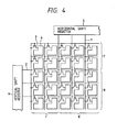
- Fig. 4 shows an
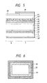
embodiment 1 invention, wherein shown aredisplay lines 1;scanning lines 2; TFT (thin film transistor)elements 3;pixel electrodes 4; ahorizontal shift register 5; a vertical shift register 6;dummy pixel rows 7; dummy pixel columns 7'; and a display area 8 x 8". Each dummy pixel is in an electrically insulated state, by not making the contact between the gate or source of theTFT element 3 and thescanning line 2 or thedisplay line 1. This embodiment employs TFT elements as switching elements, and two display lines and two scanning lines are assigned for dummy pixels. By surrounding the display area with a dummy area as explained above, same orientation of the liquid crystal can be obtained in the end portions of the display area as in the central portion thereof, and image display of high quality can be attained. - Fig. 5 shows an end portion of the device of an
embodiment 2, wherein shown are aTFT substrate 21; insulatinglayers 22, 22';alignment films 23, 23';liquid crystal 24; a sealingmaterial 25; acounter electrode 26; acolor filter 27; apolarizing plate 28; and ashield plate 29. In the present embodiment, threepixel electrodes 4 at the right-hand end constitute dummy pixels. In said dummy pixels, the TFT element (not shown) connected to each pixel electrode is connected to a scanning line and a display line, either of which is however not connected to the driving circuit, whereby said dummy pixels are maintained in electrically insulated state. Also the color filters corresponding to three pixels at the right-hand end constitute dummy filters. - Extremely splendid image display can be ensured by adopting a dummy structure same as in the display area not only on the TFT substrate but also on the opposed substrate.
- The configuration of the present invention is particularly effective in case of color display, since even a slight perturbation in orientation appears conspicuously as a variation in color.
- Fig. 6 shows an
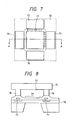
embodiment 3 of the present invention, which is additionally equipped, in the configuration of theembodiment 2, with an opaque layer. As shown in Fig. 6, the opaque area is wider than the dummy area, and thedisplay area 33 is defined by an aperture in said opaque area. The insulation state of the dummy area is same as in theembodiment 2. In this embodiment the display area is surrounded by a completely black area, so that the displayed image appears sharper. - Fig. 7 is a schematic plan view of a liquid crystal display device of the present embodiment, and Fig. 8 is a schematic cross-sectional view along a line A-A' in Fig. 7. In Figs. 7 and 8 there are shown a
pixel area 71 including vertical signal lines, horizontal gate lines and a two-dimensional array of transistor switches positioned at the crossing points of said lines, for transferring signals to the corresponding pixel electrodes; ahorizontal scanning circuit 72; avertical scanning circuit 73 having a same atep as that of saidhorizontal scanning circuit 72; ahorizontal dammy circuit 74 having a same step as that of saidhorizontal scanning circuit 72; avertical dummy circuit 75 having a same step as that of saidhorizontal scanning circuit 72; a liquidcrystal seal area 76;liquid crystal 77; asemiconductor substrate 78; and acounter substrate 79. - A
semiconductor substrate 78 consists of a Si substrate, prepared by a process shown in Figs. 9A to 9D. Said Si substrate consists of a Si monocrystalline substrate which is inexpensive, and uniform and flat over a large area, with extremely excellent crystallinity. As semiconductor active elements are formed on a monocrystalline Si layer with very little defects, the floating capacity of said semiconductor elements can be reduced. Thus there can be provided a liquid crystal display unit of high performance, in which elements and circuits capable of high-speed operation, with excellent antiradiation characteristics and without latch-up phenomenon, are integrated with the liquid crystal display pixels on a same substrate. - In the following there will be explained an example of the manufacturing method of the Si substrate according to Figs. 9A to 9D.
- A P-type (100) monocrystalline Si substrate of a thickness of 300 microns was subjected to anodization in HF solution to form a
porous Si substrate 101. - Said anodization was conducted under the following conditions:
voltage applied: 2.6 V current density: 30 mA·cm-2 anodizing solution: HF : H2O : C2H5OH = 1 : 1 : 1 duration: 2.4 hours thickness of porous Si: 300 µm porosity: 56 % - On the P-type (100)
porous Si substrate 101 thus prepared, aSi epitaxial layer 102 was grown with a thickness of 1.0 micron, by low pressure CVD. The conditions of deposition were as follows:source gas: SiH4 carrier gas: H2 temperature: 850°C pressure: 1 x 10⁻² Torr growth rate: 3.3 nm/sec. - Subsequently an
oxide layer 103 of a thickness of 1000 Å was formed on said epitaxial layer 102 (Fig. 9A). Then, theother Si substrate 107 on which anoxide layer 104 of a thickness of 5000 Å and anitride layer 105 of a thickness of 1000 Å were formed was superposed and two Si substrates were firmly adhered by heating for 0.5 hours at 800°C in nitrogen atmosphere (Fig. 9B). - Then said adhered substrates were subjected to selective etching in a mixture of 49% hydrofluoric acid, alcohol and 30% hydroperoxide (10 : 6 : 50) without agitation. After 65 minutes, the
porous Si substrate 101 was completely etched off, with the monocrystalline Si functioning as the etch stopping material, so that the non-porous Si layer alone remained. The etch rate of non-porous monocrystalline Si in the above-mentioned etching solution was very low, and the etched thickness was less than 50 Å even after 65 minutes. In fact the selective ratio of each rate to the porous layer was 10-5 or less, so that the etched amount (several tens of Angstroms) in the non-porous layer was practically negligible. Thus theporosified Si substrate 101 of a thickness of 200 µ was eliminated, and amonocrystalline Si layer 102 of a thickness of 1.0 µm could be formed on the SiO2 layer 103. When the source gas was composed of SiH2Cl, the growth temperature had to be elevated by several tens of degrees, but the elevated etching property specific to the porous substrate was maintained (see Fig. 9C. It is to be noted that Fig. 9C is shown upside down with respect to Fig. 9B). - Then TFT's were formed on said
monocrystalline silicon film 102, then the Si substrate was covered with rubber resistant to hydrofluoric acid except for the areas directly under the liquid crystal pixel areas, and the silicon substrate was locally removed to the insulation layer by means of a mixture of hydrofluoric acid, acetic acid and nitric acid thereby forming translucent areas 110. In this manner there could be obtained a substrate with TFT as shown in Fig. 9D. - The
semiconductor substrate 8 may be composed of quartz glass instead of Si wafer, but the present invention is particularly effective in case of the monocrystalline Si substrate which is difficult to planarize as explained above. - The present embodiment can provide a uniform liquid crystal cell gap, because patterns 72 - 75 of a same step are provided on the four sides of a
pixel area 71 on thesemiconductor substrate 78, and liquidcrystal sealing areas 76 are provided on said patterns. Also the chip size can be made smaller because said sealingareas 76 are formed on theperipheral scanning circuits dummy circuits peripheral scanning circuits - Naturally the displayed image quality was excellent as in the foregoing embodiments.
- Fig. 10 is a plan view of a liquid crystal display device of the present embodiment, wherein shown ' are a
display area 81 including vertical signal lines, horizontal gate lines and a two-dimensional array of transistor switches arranged at the crossing points of said lines, for transferring signals to pixel electrodes; ahorizontal scanning circuit 82 for entering image signals to odd signal lines; ahorizontal scanning circuit 83 for entering image signals to even signal lines; avertical scanning circuit 84 for entering gate signals to odd gate lines; avertical scanning circuit 85 for entering gate signals to even gate lines; and a liquidcrystal sealing area 86, said scanning circuits 82-85 having a same step height. - In the present embodiment, patterns 82 - 85 of a same step height are positioned on the four sides of the
display area 81, and are all utilized as peripheral scanning circuits. Also this embodiment, like theembodiment 4, can achieve a uniform liquid crystal cell gap and a reduced chip size, because the liquidcrystal sealing area 86 is formed on the peripheral scanning circuits 82 - 85 of a same step height. - Also in this embodiment the quality of the displayed image was excellent over the entire display area.
- Fig. 11 is a plan view of a liquid crystal display device of the present embodiment, wherein shown are a display area 91 including vertical signal lines, horizontal gate lines, and a two-dimensional array of transistor switches arranged at the crossing points of said lines, for transferring signals to pixel electrodes; a horizontal scanning circuit 92; a
vertical scanning circuit 93 for entering gate signals to odd gate lines; avertical scanning circuit 94, having a same step height as that of thevertical scanning circuit 93, for entering gate signals to even gate lines; and a liquidcrystal sealing area 95. - A sufficiently uniform liquid crystal cell gap can be attained, as in the present embodiment, by placing
patterns crystal sealing area 95 thereon. Also there can be attained a further reduced chip size, as will be apparent from Fig. 11. - In this embodiment, the steps are not formed on all the sides of the display area, but there can be obtained image display of extremely higher quality, in comparison with the case where such steps are absent.
- As explained in the foregoing, the liquid crystal display device of the present invention can control the orientation of liquid crystal to the end portions of the display area, thereby enabling to display image of high quality without unevenness over the entire display area, by the formation of steps such as dummy circuits in the surrounding area of the display area.
- Also the present invention can achieve power saving because an elevated driving voltage is not required, and can reduce the size of the liquid crystal display device with respect to the display area size.
- Furthermore, the present invention can provide a liquid crystal display device of a uniform cell gap, thereby providing display without unevenness in color, without increase in the chip size and without addition of extra steps in the manufacture.
- Furthermore, the present invention can provide color image display of extremely high quality, without unevenness in color even in the end portion of the display area.
- The liquid crystal sealing area may be provided on an area of a substantially same step height as that of the display area, and may naturally be provided, not only on circuit elements but also on wirings or dummy areas of a same step height.
- Also formation of an opaque area, corresponding to said stepped area, is effective for obtaining sharper image display.
- In addition, the shape of the step, to be formed adjacent to the pixel area, may be made same as, substantially same as or similar to that of said pixel area by a dummy area, a circuit element or a wiring alone or by the combination thereof.
- A liquid crystal display device comprises, at least, in a part of a close periphery of the display area of a pixel electrode substrate, a step substantially same as that of the display area.
Claims (3)
- A color liquid crystal display including a display area (8) comprising:an electrode substrate (21) provided with pixel electrodes, switching elements, scanning and display line electrodes and first alignment film (23) for the display area,a counter substrate disposed in facing said electrode substrate and provided with a counter electrode (26) which is disposed in facing each of the pixel electrodes in said electrode substrate, color filter (27) and second alignment film (23') for the display area, anda liquid crystal disposed between said electrode substrate and said counter substrate, anda light-shielding member (29) or an opaque layer,wherein said counter substrate has a dummy area (7) at least partially surrounding the display area, and the dummy area is provided with a dummy color filter to form a substantially same step as that of the display area, and said light-shielding member or said opaque layer light-shields the dummy area
characterized in thatthe first and second alignment films treated by a rubbing process extend to the dummy area. - A color liquid display according to claim 1, wherein each switching element comprises a transistor.
- A color liquid display according to claim 1, wherein each switching element comprises a thin film transistor.
Priority Applications (1)
| Application Number | Priority Date | Filing Date | Title |
|---|---|---|---|
| EP06115969A EP1703317B1 (en) | 1992-02-27 | 1993-02-26 | Liquid crystal display device |
Applications Claiming Priority (6)
| Application Number | Priority Date | Filing Date | Title |
|---|---|---|---|
| JP7557492 | 1992-02-27 | ||
| JP7557492A JP3256810B2 (en) | 1992-02-27 | 1992-02-27 | Liquid crystal display |
| JP2164193 | 1993-01-18 | ||
| JP2164193A JPH06214241A (en) | 1993-01-18 | 1993-01-18 | Liquid crystal display device |
| EP93103103A EP0558058B1 (en) | 1992-02-27 | 1993-02-26 | Liquid crystal display device |
| EP00107887A EP1022603B1 (en) | 1992-02-27 | 1993-02-26 | Liquid crystal display device |
Related Parent Applications (1)
| Application Number | Title | Priority Date | Filing Date |
|---|---|---|---|
| EP00107887A Division EP1022603B1 (en) | 1992-02-27 | 1993-02-26 | Liquid crystal display device |
Related Child Applications (1)
| Application Number | Title | Priority Date | Filing Date |
|---|---|---|---|
| EP06115969A Division EP1703317B1 (en) | 1992-02-27 | 1993-02-26 | Liquid crystal display device |
Publications (2)
| Publication Number | Publication Date |
|---|---|
| EP1507162A1 EP1507162A1 (en) | 2005-02-16 |
| EP1507162B1 true EP1507162B1 (en) | 2007-01-10 |
Family
ID=26358730
Family Applications (8)
| Application Number | Title | Priority Date | Filing Date |
|---|---|---|---|
| EP00107887A Expired - Lifetime EP1022603B1 (en) | 1992-02-27 | 1993-02-26 | Liquid crystal display device |
| EP93103103A Expired - Lifetime EP0558058B1 (en) | 1992-02-27 | 1993-02-26 | Liquid crystal display device |
| EP04012642A Withdrawn EP1473585A1 (en) | 1992-02-27 | 1993-02-26 | Liquid crystal display device |
| EP03016342A Withdrawn EP1378785A3 (en) | 1992-02-27 | 1993-02-26 | Liquid crystal display device |
| EP06115969A Expired - Lifetime EP1703317B1 (en) | 1992-02-27 | 1993-02-26 | Liquid crystal display device |
| EP04022587A Expired - Lifetime EP1507162B1 (en) | 1992-02-27 | 1993-02-26 | Liquid crystal display device |
| EP00100574A Expired - Lifetime EP1003065B1 (en) | 1992-02-27 | 1993-02-26 | Liquid crystal display device |
| EP00107888A Expired - Lifetime EP1022604B1 (en) | 1992-02-27 | 1993-02-26 | Liquid crystal display device |
Family Applications Before (5)
| Application Number | Title | Priority Date | Filing Date |
|---|---|---|---|
| EP00107887A Expired - Lifetime EP1022603B1 (en) | 1992-02-27 | 1993-02-26 | Liquid crystal display device |
| EP93103103A Expired - Lifetime EP0558058B1 (en) | 1992-02-27 | 1993-02-26 | Liquid crystal display device |
| EP04012642A Withdrawn EP1473585A1 (en) | 1992-02-27 | 1993-02-26 | Liquid crystal display device |
| EP03016342A Withdrawn EP1378785A3 (en) | 1992-02-27 | 1993-02-26 | Liquid crystal display device |
| EP06115969A Expired - Lifetime EP1703317B1 (en) | 1992-02-27 | 1993-02-26 | Liquid crystal display device |
Family Applications After (2)
| Application Number | Title | Priority Date | Filing Date |
|---|---|---|---|
| EP00100574A Expired - Lifetime EP1003065B1 (en) | 1992-02-27 | 1993-02-26 | Liquid crystal display device |
| EP00107888A Expired - Lifetime EP1022604B1 (en) | 1992-02-27 | 1993-02-26 | Liquid crystal display device |
Country Status (3)
| Country | Link |
|---|---|
| US (1) | US5513028A (en) |
| EP (8) | EP1022603B1 (en) |
| DE (6) | DE69330318T2 (en) |
Families Citing this family (39)
| Publication number | Priority date | Publication date | Assignee | Title |
|---|---|---|---|---|
| EP0609809B8 (en) * | 1993-02-01 | 2001-11-21 | Canon Kabushiki Kaisha | Liquid crystal display device |
| JP2885093B2 (en) * | 1994-10-17 | 1999-04-19 | 日本電気株式会社 | Image display method |
| US5936694A (en) * | 1995-04-26 | 1999-08-10 | Canon Kabushiki Kaisha | Liquid crystal device and process for producing same |
| JP3256834B2 (en) * | 1995-06-01 | 2002-02-18 | キヤノン株式会社 | Liquid crystal display |
| JP3205767B2 (en) * | 1995-09-13 | 2001-09-04 | キヤノン株式会社 | Transmissive liquid crystal display |
| JP3143592B2 (en) * | 1995-09-14 | 2001-03-07 | キヤノン株式会社 | Display device |
| JPH09138390A (en) * | 1995-09-14 | 1997-05-27 | Canon Inc | Liquid crystal display device |
| JP3143591B2 (en) * | 1995-09-14 | 2001-03-07 | キヤノン株式会社 | Display device |
| JP3737176B2 (en) * | 1995-12-21 | 2006-01-18 | 株式会社半導体エネルギー研究所 | Liquid crystal display |
| JPH09292633A (en) * | 1996-02-27 | 1997-11-11 | Canon Inc | Production of color liquid crystal display device |
| US7298447B1 (en) | 1996-06-25 | 2007-11-20 | Semiconductor Energy Laboratory Co., Ltd. | Liquid crystal display panel |
| KR100228282B1 (en) * | 1996-09-17 | 1999-11-01 | 윤종용 | Liquid display device |
| JP3249077B2 (en) * | 1996-10-18 | 2002-01-21 | キヤノン株式会社 | Matrix substrate and liquid crystal device |
| JP4147594B2 (en) * | 1997-01-29 | 2008-09-10 | セイコーエプソン株式会社 | Active matrix substrate, liquid crystal display device, and electronic device |
| US6177969B1 (en) | 1997-03-21 | 2001-01-23 | Canon Kabushiki Kaisha | Matrix substrate and liquid crystal display device utilizing the same in which a conductive film in an aperture region opposes the side the switching elements are on |
| TW375689B (en) * | 1997-03-27 | 1999-12-01 | Toshiba Corp | Liquid crystal display device and method for manufacturing the same |
| TW500937B (en) | 1999-07-13 | 2002-09-01 | Samsung Electronics Co Ltd | Liquid crystal display |
| KR100582598B1 (en) * | 2000-10-25 | 2006-05-23 | 엘지.필립스 엘시디 주식회사 | Liquid Crystal Display Device Preventing From Leakage Light |
| US6961029B1 (en) * | 2000-11-08 | 2005-11-01 | Palm, Inc. | Pixel border for improved viewability of a display device |
| US7724270B1 (en) | 2000-11-08 | 2010-05-25 | Palm, Inc. | Apparatus and methods to achieve a variable color pixel border on a negative mode screen with a passive matrix drive |
| US7425970B1 (en) | 2000-11-08 | 2008-09-16 | Palm, Inc. | Controllable pixel border for a negative mode passive matrix display device |
| US6414337B1 (en) * | 2000-11-10 | 2002-07-02 | Three-Five Systems, Inc. | Aperture frame for liquid crystal display device |
| KR100685916B1 (en) * | 2000-12-22 | 2007-02-23 | 엘지.필립스 엘시디 주식회사 | Liquid crystal display panel |
| KR100394026B1 (en) * | 2000-12-27 | 2003-08-06 | 엘지.필립스 엘시디 주식회사 | Liquid crystal device and method for driving the same |
| JP4544809B2 (en) * | 2001-07-18 | 2010-09-15 | 三星電子株式会社 | Liquid crystal display |
| JPWO2003030131A1 (en) | 2001-08-29 | 2005-01-20 | セイコーエプソン株式会社 | Electro-optical device and electronic apparatus |
| JP4003471B2 (en) * | 2002-02-12 | 2007-11-07 | セイコーエプソン株式会社 | Electro-optical device, electronic apparatus, and method of manufacturing electro-optical device |
| KR100480332B1 (en) * | 2002-04-08 | 2005-04-06 | 엘지.필립스 엘시디 주식회사 | Liquid Crystal Panel used for a Liquid Crystal Display Device |
| KR100878790B1 (en) * | 2002-09-05 | 2009-01-14 | 삼성전자주식회사 | Active matrix driving display device and image displaying method using the same |
| US7053649B1 (en) | 2002-12-06 | 2006-05-30 | Semiconductor Energy Laboratory Co., Ltd. | Image display device and method of testing the same |
| US7265572B2 (en) | 2002-12-06 | 2007-09-04 | Semicondcutor Energy Laboratory Co., Ltd. | Image display device and method of testing the same |
| JP4759925B2 (en) * | 2004-03-19 | 2011-08-31 | セイコーエプソン株式会社 | Electro-optical device and electronic apparatus |
| JP4111195B2 (en) * | 2005-01-26 | 2008-07-02 | セイコーエプソン株式会社 | Device, manufacturing method thereof, electro-optical device, manufacturing method thereof, and electronic apparatus |
| US20090073099A1 (en) * | 2007-09-14 | 2009-03-19 | Tpo Displays Corp. | Display comprising a plurality of pixels and a device comprising such a display |
| KR101300034B1 (en) | 2010-10-18 | 2013-08-29 | 엘지디스플레이 주식회사 | Substrate for liquid crystal display device and apparatus using the same |
| KR102013161B1 (en) | 2012-08-20 | 2019-08-23 | 삼성디스플레이 주식회사 | Back light assembly and display apparatus having the same |
| KR102252443B1 (en) * | 2015-01-08 | 2021-05-14 | 삼성디스플레이 주식회사 | Liquid crystal display device |
| CN109119013A (en) * | 2018-09-07 | 2019-01-01 | 武汉天马微电子有限公司 | Driving method, display panel and the display device of display panel |
| CN110716359A (en) * | 2019-10-14 | 2020-01-21 | 深圳市华星光电技术有限公司 | Array substrate, manufacturing method thereof and alignment precision detection method |
Family Cites Families (12)
| Publication number | Priority date | Publication date | Assignee | Title |
|---|---|---|---|---|
| JPS5895327A (en) * | 1981-12-01 | 1983-06-06 | Alps Electric Co Ltd | Color liquid crystal display element |
| JPS60243638A (en) * | 1984-05-18 | 1985-12-03 | Seiko Epson Corp | Liquid crystal color display device |
| FR2585162B1 (en) * | 1985-07-19 | 1991-03-08 | Gen Electric | CELL SPACER HOLDING AND LIGHT LOCKING STRUCTURE FOR LIQUID CRYSTAL MATRIX DISPLAYS |
| JPH01257823A (en) * | 1988-04-07 | 1989-10-13 | Dainippon Printing Co Ltd | Color filter substrate for liquid crystal display device |
| DE68921910T3 (en) * | 1988-04-21 | 2000-08-17 | Asahi Glass Co Ltd | Color liquid crystal display device and its driving method. |
| JPH02123325A (en) * | 1988-11-01 | 1990-05-10 | Asahi Glass Co Ltd | Color liquid crystal display device |
| JPH0287116A (en) * | 1988-09-26 | 1990-03-28 | Dainippon Printing Co Ltd | Base plate for color filter for liquid crystal display device |
| US5040041A (en) * | 1988-10-20 | 1991-08-13 | Canon Kabushiki Kaisha | Semiconductor device and signal processing device having said device provided therein |
| GB2235326A (en) * | 1989-08-16 | 1991-02-27 | Philips Electronic Associated | Active matrix liquid crystal colour display devices |
| JP2638237B2 (en) * | 1989-12-28 | 1997-08-06 | カシオ計算機株式会社 | Liquid crystal element |
| JP2872321B2 (en) * | 1990-01-17 | 1999-03-17 | 株式会社日立製作所 | Liquid crystal display device |
| KR960014823B1 (en) * | 1991-03-15 | 1996-10-21 | 가부시기가이샤 히다찌세이사구쇼 | Liquid crystal display device |
-
1993
- 1993-02-26 DE DE69330318T patent/DE69330318T2/en not_active Expired - Lifetime
- 1993-02-26 EP EP00107887A patent/EP1022603B1/en not_active Expired - Lifetime
- 1993-02-26 EP EP93103103A patent/EP0558058B1/en not_active Expired - Lifetime
- 1993-02-26 DE DE69333753T patent/DE69333753T2/en not_active Expired - Lifetime
- 1993-02-26 EP EP04012642A patent/EP1473585A1/en not_active Withdrawn
- 1993-02-26 DE DE69333192T patent/DE69333192T2/en not_active Expired - Lifetime
- 1993-02-26 EP EP03016342A patent/EP1378785A3/en not_active Withdrawn
- 1993-02-26 EP EP06115969A patent/EP1703317B1/en not_active Expired - Lifetime
- 1993-02-26 EP EP04022587A patent/EP1507162B1/en not_active Expired - Lifetime
- 1993-02-26 EP EP00100574A patent/EP1003065B1/en not_active Expired - Lifetime
- 1993-02-26 DE DE69333137T patent/DE69333137T2/en not_active Expired - Lifetime
- 1993-02-26 EP EP00107888A patent/EP1022604B1/en not_active Expired - Lifetime
- 1993-02-26 DE DE69334236T patent/DE69334236D1/en not_active Expired - Lifetime
- 1993-02-26 DE DE69334103T patent/DE69334103T2/en not_active Expired - Fee Related
-
1995
- 1995-04-10 US US08/419,762 patent/US5513028A/en not_active Expired - Lifetime
Also Published As
| Publication number | Publication date |
|---|---|
| DE69333192D1 (en) | 2003-10-09 |
| EP1378785A2 (en) | 2004-01-07 |
| EP1473585A1 (en) | 2004-11-03 |
| EP1378785A3 (en) | 2004-10-20 |
| EP1703317A1 (en) | 2006-09-20 |
| EP1022604A2 (en) | 2000-07-26 |
| EP1022604B1 (en) | 2003-09-03 |
| EP1003065A3 (en) | 2001-02-07 |
| DE69333137D1 (en) | 2003-09-11 |
| EP1003065A2 (en) | 2000-05-24 |
| DE69333753T2 (en) | 2006-05-11 |
| EP1003065B1 (en) | 2003-08-06 |
| EP0558058A1 (en) | 1993-09-01 |
| US5513028A (en) | 1996-04-30 |
| DE69334236D1 (en) | 2008-09-18 |
| EP1022603A3 (en) | 2001-10-24 |
| DE69333192T2 (en) | 2004-07-15 |
| EP1507162A1 (en) | 2005-02-16 |
| DE69333137T2 (en) | 2004-06-09 |
| DE69330318D1 (en) | 2001-07-19 |
| EP1022604A3 (en) | 2001-02-14 |
| DE69330318T2 (en) | 2001-10-31 |
| DE69334103T2 (en) | 2007-10-25 |
| EP1022603B1 (en) | 2005-02-02 |
| EP1703317B1 (en) | 2008-08-06 |
| DE69334103D1 (en) | 2007-02-22 |
| EP1022603A2 (en) | 2000-07-26 |
| DE69333753D1 (en) | 2005-03-10 |
| EP0558058B1 (en) | 2001-06-13 |
Similar Documents
| Publication | Publication Date | Title |
|---|---|---|
| EP1507162B1 (en) | Liquid crystal display device | |
| US6614500B2 (en) | Liquid crystal display having a dummy source pad and method for manufacturing the same | |
| US6040200A (en) | Method of fabricating semiconductor device having stacked-layered substrate | |
| US7868984B2 (en) | Electro-optical device and method of manufacturing the same | |
| JPH08179377A (en) | Reflection type active matrix display panel and its production | |
| US5644373A (en) | Liquid crystal device with substrates of different materials and similar thermal expansion coefficients | |
| US5349453A (en) | Liquid crystal display device with microlenses on same plane as switching elements | |
| US6995812B2 (en) | Liquid crystal display device | |
| US6331473B1 (en) | SOI substrate, method for making the same, semiconductive device and liquid crystal panel using the same | |
| KR100326691B1 (en) | Method of manufacturing a reflective display | |
| JP3305085B2 (en) | Liquid crystal display | |
| JP2979196B2 (en) | Semiconductor substrate device for light valve and method of manufacturing the same | |
| JPH02198428A (en) | Active matrix substrate for liquid crystal display device | |
| JPH06214241A (en) | Liquid crystal display device | |
| JPH0862629A (en) | Liquid crystal display device | |
| JPH0385529A (en) | Thin-film semiconductor display device | |
| JP3023729B2 (en) | Liquid crystal display | |
| JPH0961851A (en) | Liquid crystal display device | |
| KR100268302B1 (en) | Lcd structure and its fabrication method | |
| JPH04133034A (en) | Single crystal thin film semiconductor device for optical valve substrate | |
| JPH0542832B2 (en) | ||
| JPH05181164A (en) | Active matrix substrate and its manufacture | |
| JPH07168170A (en) | Liquid crystal display device | |
| JPH05127190A (en) | Semiconductor device for light valve substrate and production thereof | |
| JPH0968725A (en) | Polysilicon thin-film transistor and liquid crystal display device |
Legal Events
| Date | Code | Title | Description |
|---|---|---|---|
| PUAI | Public reference made under article 153(3) epc to a published international application that has entered the european phase |
Free format text: ORIGINAL CODE: 0009012 |
|
| AC | Divisional application: reference to earlier application |
Ref document number: 1022603 Country of ref document: EP Kind code of ref document: P Ref document number: 0558058 Country of ref document: EP Kind code of ref document: P |
|
| AK | Designated contracting states |
Kind code of ref document: A1 Designated state(s): DE FR GB |
|
| 17P | Request for examination filed |
Effective date: 20050812 |
|
| AKX | Designation fees paid |
Designated state(s): DE FR GB |
|
| GRAP | Despatch of communication of intention to grant a patent |
Free format text: ORIGINAL CODE: EPIDOSNIGR1 |
|
| GRAS | Grant fee paid |
Free format text: ORIGINAL CODE: EPIDOSNIGR3 |
|
| GRAA | (expected) grant |
Free format text: ORIGINAL CODE: 0009210 |
|
| AC | Divisional application: reference to earlier application |
Ref document number: 1022603 Country of ref document: EP Kind code of ref document: P Ref document number: 0558058 Country of ref document: EP Kind code of ref document: P |
|
| AK | Designated contracting states |
Kind code of ref document: B1 Designated state(s): DE FR GB |
|
| REG | Reference to a national code |
Ref country code: GB Ref legal event code: FG4D |
|
| REF | Corresponds to: |
Ref document number: 69334103 Country of ref document: DE Date of ref document: 20070222 Kind code of ref document: P |
|
| ET | Fr: translation filed | ||
| PLBE | No opposition filed within time limit |
Free format text: ORIGINAL CODE: 0009261 |
|
| STAA | Information on the status of an ep patent application or granted ep patent |
Free format text: STATUS: NO OPPOSITION FILED WITHIN TIME LIMIT |
|
| 26N | No opposition filed |
Effective date: 20071011 |
|
| PGFP | Annual fee paid to national office [announced via postgrant information from national office to epo] |
Ref country code: DE Payment date: 20090228 Year of fee payment: 17 |
|
| PGFP | Annual fee paid to national office [announced via postgrant information from national office to epo] |
Ref country code: FR Payment date: 20090223 Year of fee payment: 17 |
|
| REG | Reference to a national code |
Ref country code: FR Ref legal event code: ST Effective date: 20101029 |
|
| PG25 | Lapsed in a contracting state [announced via postgrant information from national office to epo] |
Ref country code: FR Free format text: LAPSE BECAUSE OF NON-PAYMENT OF DUE FEES Effective date: 20100301 |
|
| PG25 | Lapsed in a contracting state [announced via postgrant information from national office to epo] |
Ref country code: DE Free format text: LAPSE BECAUSE OF NON-PAYMENT OF DUE FEES Effective date: 20100901 |
|
| PGFP | Annual fee paid to national office [announced via postgrant information from national office to epo] |
Ref country code: GB Payment date: 20110224 Year of fee payment: 19 |
|
| GBPC | Gb: european patent ceased through non-payment of renewal fee |
Effective date: 20120226 |
|
| PG25 | Lapsed in a contracting state [announced via postgrant information from national office to epo] |
Ref country code: GB Free format text: LAPSE BECAUSE OF NON-PAYMENT OF DUE FEES Effective date: 20120226 |