EP1505729A2 - Conductive adhesive and piezoelectric device using it - Google Patents
Conductive adhesive and piezoelectric device using it Download PDFInfo
- Publication number
- EP1505729A2 EP1505729A2 EP04018721A EP04018721A EP1505729A2 EP 1505729 A2 EP1505729 A2 EP 1505729A2 EP 04018721 A EP04018721 A EP 04018721A EP 04018721 A EP04018721 A EP 04018721A EP 1505729 A2 EP1505729 A2 EP 1505729A2
- Authority
- EP
- European Patent Office
- Prior art keywords
- conductive filler
- conductive adhesive
- conductive
- bonding
- base
- Prior art date
- Legal status (The legal status is an assumption and is not a legal conclusion. Google has not performed a legal analysis and makes no representation as to the accuracy of the status listed.)
- Withdrawn
Links
Images



Classifications
-
- H—ELECTRICITY
- H03—ELECTRONIC CIRCUITRY
- H03H—IMPEDANCE NETWORKS, e.g. RESONANT CIRCUITS; RESONATORS
- H03H9/00—Networks comprising electromechanical or electro-acoustic elements; Electromechanical resonators
- H03H9/02—Details
- H03H9/05—Holders or supports
- H03H9/10—Mounting in enclosures
- H03H9/1064—Mounting in enclosures for surface acoustic wave [SAW] devices
- H03H9/1071—Mounting in enclosures for surface acoustic wave [SAW] devices the enclosure being defined by a frame built on a substrate and a cap, the frame having no mechanical contact with the SAW device
-
- H—ELECTRICITY
- H10—SEMICONDUCTOR DEVICES; ELECTRIC SOLID-STATE DEVICES NOT OTHERWISE PROVIDED FOR
- H10W—GENERIC PACKAGES, INTERCONNECTIONS, CONNECTORS OR OTHER CONSTRUCTIONAL DETAILS OF DEVICES COVERED BY CLASS H10
- H10W72/00—Interconnections or connectors in packages
- H10W72/071—Connecting or disconnecting
-
- H—ELECTRICITY
- H03—ELECTRONIC CIRCUITRY
- H03H—IMPEDANCE NETWORKS, e.g. RESONANT CIRCUITS; RESONATORS
- H03H9/00—Networks comprising electromechanical or electro-acoustic elements; Electromechanical resonators
- H03H9/02—Details
- H03H9/05—Holders or supports
- H03H9/058—Holders or supports for surface acoustic wave devices
- H03H9/0585—Holders or supports for surface acoustic wave devices consisting of an adhesive layer
-
- H—ELECTRICITY
- H10—SEMICONDUCTOR DEVICES; ELECTRIC SOLID-STATE DEVICES NOT OTHERWISE PROVIDED FOR
- H10W—GENERIC PACKAGES, INTERCONNECTIONS, CONNECTORS OR OTHER CONSTRUCTIONAL DETAILS OF DEVICES COVERED BY CLASS H10
- H10W72/00—Interconnections or connectors in packages
- H10W72/071—Connecting or disconnecting
- H10W72/075—Connecting or disconnecting of bond wires
- H10W72/07521—Aligning
-
- H—ELECTRICITY
- H10—SEMICONDUCTOR DEVICES; ELECTRIC SOLID-STATE DEVICES NOT OTHERWISE PROVIDED FOR
- H10W—GENERIC PACKAGES, INTERCONNECTIONS, CONNECTORS OR OTHER CONSTRUCTIONAL DETAILS OF DEVICES COVERED BY CLASS H10
- H10W72/00—Interconnections or connectors in packages
- H10W72/50—Bond wires
- H10W72/531—Shapes of wire connectors
- H10W72/5363—Shapes of wire connectors the connected ends being wedge-shaped
-
- H—ELECTRICITY
- H10—SEMICONDUCTOR DEVICES; ELECTRIC SOLID-STATE DEVICES NOT OTHERWISE PROVIDED FOR
- H10W—GENERIC PACKAGES, INTERCONNECTIONS, CONNECTORS OR OTHER CONSTRUCTIONAL DETAILS OF DEVICES COVERED BY CLASS H10
- H10W72/00—Interconnections or connectors in packages
- H10W72/50—Bond wires
- H10W72/551—Materials of bond wires
- H10W72/552—Materials of bond wires comprising metals or metalloids, e.g. silver
- H10W72/5524—Materials of bond wires comprising metals or metalloids, e.g. silver comprising aluminium [Al]
-
- H—ELECTRICITY
- H10—SEMICONDUCTOR DEVICES; ELECTRIC SOLID-STATE DEVICES NOT OTHERWISE PROVIDED FOR
- H10W—GENERIC PACKAGES, INTERCONNECTIONS, CONNECTORS OR OTHER CONSTRUCTIONAL DETAILS OF DEVICES COVERED BY CLASS H10
- H10W72/00—Interconnections or connectors in packages
- H10W72/851—Dispositions of multiple connectors or interconnections
- H10W72/874—On different surfaces
- H10W72/884—Die-attach connectors and bond wires
Definitions
- This invention relates to a conductive adhesive suited for a structure of a piezoelectric device, for example, with a piezoelectric element such as an SAW (surface acoustic wave) device bonded and affixed to inside a package.
- the invention also relates to a piezoelectric device using the conductive adhesive for bonding its piezoelectric element.
- the SAW device has a package in which a metallic lid is hermetically joined and sealed by seam welding, via a seal ring, to an upper end of a base made up of a ceramic material, and an SAW element is mounted therein.
- the SAW element has its lower surface bonded and affixed with an adhesive to an empty bottom surface on the base, while each bonding pad for electrode connection provided on an upper surface thereof is electrically connected to a corresponding connection terminal in the package through a bonding wire.
- a bonding wire of an aluminum type material there is typically used a bonding wire of an aluminum type material, and its tip is joined to a bonding pad surface by a wedge bonding method that performs joining by applying ultrasonic vibration while pressurizing with a wedge tool as disclosed in JP-A-2003-110401, for example.
- the metallic lid reaches a high temperature of approx. 200 to 500°C due to heat generated at the time of seam welding, hence, fused joining of it is carried out in a thermally expanded state more than that of the ceramic base that has a small thermal expansion rate.
- the lid contracts more than the base. Consequently, stress is generated in the base such as to deform it downward convex. This deformation is conveyed to the SAW element through the adhesive, possibly affecting its characteristics adversely. Although the adhesive somewhat contracts when it is baked and hardened, stress due to this will also act on the SAW element. These stresses are not desirable in terms of achieving high frequency and high precision.
- SAW devices one having a structure in which an SAW element is bonded and affixed to only the central part of the base of a package or bonded and affixed by an elastic adhesive or through a buffer material, and another one having a structure in which a silicon resin layer is formed on the bottom surface of a cavity of a package and an SAW element is bonded and affixed thereon by using an elastic adhesive so as to absorb stress such as thermal distortion due to seam welding (JP-A-6-177701 and JP-A-2002-16476).
- an adhesive for bonding and affixing an SAW element requires, subsequent to hardening thereof, a softness which can sufficiently absorb thermal deformation due to seam welding and stress due to contraction during hardening of the adhesive, for example, i.e., a low elastic modulus of under 0.1GPa.
- an elastic conductive adhesive conventionally used to bond and affix an SAW element is obtained by adding typically three kinds of conductive fillers different in shape and dimension, for example, a small particle conductive filler of a particle diameter of 2.2-6.2 ⁇ m, a large particle conductive filler of a particle diameter of 8.2-14.3 ⁇ m, and a small flaky conductive filler of 2.2-4.4 ⁇ m in length, to a silicon type resin material at an appropriate ratio, for example, 22.5/77.5 % by weight.
- these three conductive fillers are unevenly distributed and there is a lot of elastic resin material among the fillers.
- Such elastic conductive adhesive when a bonding wire tip is pressed to a bonding pad surface by the wedge tool, may undergo elastic deformation unnecessarily so that an SAW element may possibly sink heavily. Since the joint state of a bonding wire bonded by the wedge bonding method is determined by the ultrasonic output, the load on the bonding wire, the processing time, and the balance of these, if the SAW element sinks too much, the load on the bonding wire and ultrasonic vibration disappear, thereby creating a problem of making it impossible to get a proper state of joint.
- the conductive filler is constituted by a flaky conductive filler, in manufacturing a piezoelectric device, upon pressurizing and bonding the piezoelectric element to the conductive adhesive on a mounting surface of a base, flakes of the conductive filler arrange mutually in close proximity to one another piling up in the conductive adhesive after hardening, so that a much smaller amount of the resin material exists between the flakes of the conductive than conventionally.
- the conductive adhesive after hardening undergoes less elastic deformation, thereby reducing the sinkage of the piezoelectric element to a large extent and enhancing bondability. Consequently, it is possible to connect the bonding wires in the proper state of joint.
- the conductive filler is composed of two kinds of large and small particulate conductive fillers, likewise, in manufacturing the piezoelectric device, when the piezoelectric element is pressed and bonded to the conductive adhesive on the mounting surface of the adhesive base, the particles of the conductive fillers are evenly distributed with those of the small particulate conductive fillers filling the gaps between adjacent ones of those of large particulate conductive fillers, one on top of another.
- the amount of resin material existing between the conductive filler particles becomes smaller than conventionally, so that, when pressurizing by the wedge tool from above in subjecting the piezoelectric element to wire bonding, the conductive adhesive after hardening is able to cause less elastic deformation, while maintaining sufficient softness.
- FIGs. 1A and 1B show an embodiment of an SAW device to which this invention is applied.
- This SAW device has a package 4 composed of a rectangular box-shaped base 1 whose upper part is hermetically closed by a lid 2 of a thin metallic plate. The lid 2 is joined to an upper end of the base 1 by seam welding through a seal ring 3.
- An SAW element 5 is mounted and sealed in the package 4.
- the base 1 is a multi-layer structure of a plurality of thin plates of a ceramic material such as alumina.
- the empty space has a first portion, whose bottom defines the mounting surface 6, and a second portion on either side, in the width direction, of the first portion.
- the first portion is deeper than the second portions so that steps are formed on both sides of the deeper first portion.
- the SAW element 5 has IDTs formed on the center of an upper surface of a rectangular piezoelectric substrate made of a material such as quartz, lithium tantalate, or lithium niobate.
- the IDTs consist of a pair of inter digital electrodes 8, and a respective grid-like reflector 9 formed on each of both sides in the length direction.
- Each of the inter digital electrodes 8 has, in continuation with its bus bar, a bonding pad 10 in proximity to the longitudinal periphery of the substrate.
- the inter digital electrodes, the reflectors, and the bonding pads of this embodiment are formed of aluminum in consideration of its ease of processing and cost. However, it is possible to use other conductive metallic materials such as aluminum alloys which are typically used.
- connection terminal corresponding to a respective one of the two bonding pads 10, is formed inside the base 1 on an upper surface of each of the two steps mentioned above and, thus, on either side of the SAW element 5 in the width direction.
- Each connection terminal is electrically connected by a respective bonding wire 12 to the corresponding one of the bonding pads.
- aluminum wires of the same conductive material as the bonding pads are used.
- the connection terminals are formed, for example, by screen printing of a metallic wiring material such as W or Mo onto a surface of a thin ceramic plate of the base 1 and plating it with Ni or Au.
- the connection terminals are connected to external terminals on an outer surface of the base 1 through a wiring pattern provided on the thin ceramic plate or a via hole (not illustrated).
- the bonding wires 12 and the bonding pads 10 are connected by means of the wedge bonding method using pressurization and ultrasonic vibration, after an oxide film has been removed from the surface of the bonding pads by mechanical cleaning. As shown in FIG. 2, a tip of a bonding wire 12 is pressed onto the surface of the bonding pad 10 by a prescribed pressure, and then ultrasonic vibration is applied to join the two. After mounting the SAW element 5 and forming a connection in this way, the lid 2 is joined to the seal ring 3 on the upper end of the base 1 by seam welding and the package 4 is hermetically sealed.
- the conductive adhesive 7 is composed of 80 to 85 wt.% of a silicon type resin material and 20 to 15 wt.% of a flaky silver powder as a conductive filler.
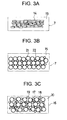
- the flakes of the conductive filler 14 are arranged as shown in FIG. 3A, i.e., side by side and one layer upon the other, with only a small amount of the resin material 15 in between.
- the conductive adhesive 7 has little elastic deformation and the SAW element 5 is sufficiently supported to reduce the sinkage to a large extent, thus improving the bondability and keeping the bonding wire to be connected in a proper joint condition at all times. Therefore, it is desirable that the conductive filler 14 contained in the conductive adhesive 7 is comprised of nothing but 100% flaky substance. However, in actuality, shapes other than flakes may be contained; as long as the proportion of flakes is virtually close to 100%, sufficient operation/working-effect of this invention may be obtained.
- the conductive filler consists of a flaky silver powder with flakes being 4.3 to 6.0 ⁇ m long, and the hardness of the conductive adhesive after hardening is under 6B and its elastic modulus after hardening is under 0.1GPa.
- FIG. 3C shows a case where a conventional silicon type conductive adhesive 16 is used for bonding and affixing the SAW element 5.
- This conventional silicon type conductive adhesive 16 is obtained by adding a conductive filler consisting of, for example, a small particulate conductive filler 17 of a particle diameter of 2.2 to 6.2 ⁇ m, a large particulate conductive filler 18 of a particle diameter of 8.2 to 14.3 ⁇ m, and a small flaky conductive filler 19, 2.2 to 4.4 ⁇ m long, to a silicon type resin material 20 at a proper ratio, for example, 22.5/77.5 wt.%.
- the hardness of the conductive adhesive 16 after hardening is under 6B and its elastic modulus after hardening is under 0.1GPa.
- the conductive adhesive 7 contains 82.5 to 80 wt.% of a resin material and 17.5 to 15 wt.% of a conductive filler.
- the conductive filler comprises 30 wt.% of a small particulate conductive filler and 70 wt.% of a large particulate conductive filler.
- the conductive filler particles are piled up one on top of another in a condition in which particles of the small particulate filler 22 are evenly distributed filling the spaces between particles of the large particulate conductive filler 21, so that the amount of the resin material 15 in between these particles is considerably smaller as compared to the conventional case.
- the conductive adhesive 7 has small elastic deformation and the SAW element 5 is sufficiently supported to reduce the sinkage to a large extent, thus improving the bondability and keeping the bonding wire to be connected in a proper joint condition at all times.
- the conductive adhesive of the first embodiment there are larger gaps between the particles of the conductive fillers such that a greater amount of resin material 15 exists therein, thus enabling sufficient softness to be secured. Consequently, the conductive adhesive 7 is able to absorb any impact from outside such as stress and a drop due to package deformation, adhesive contraction and the like, thus making it possible to secure proper operation and desired characteristics of the SAW element 5.
- the invention is not limited to the above-mentioned embodiments.
- various known materials other than silver powder may be used for the conductive filler of the conductive adhesive.
- various piezoelectric devices having packages mounted with other piezoelectric elements than a SAW element, or tuning fork type or other piezoelectric vibrating reeds the same may be applicable.
- Example 1 An SAW resonator having an SAW element bonded and affixed to the base 1 by using the conductive adhesive of the first embodiment of this invention mentioned above in connection with FIG. 3A, and, as Example 2, an SAW resonator having an SAW element bonded and affixed to the base 1 by using the conductive adhesive of the second embodiment of this invention mentioned above in connection with FIG. 3B.
- a die attachment condition or pressurizing force when bonding the SAW element to the mounting surface of the base was 20 ⁇ 15 g/cm 2 (1.961 ⁇ 1.471 kPa) for both cases, and the conductive adhesive was hardened by baking in an N 2 atmosphere at 180°C for 1 hour (Example 1), and by baking in vacuum at 280°C for 3 hours (Example 2).
- the bonding wires an Al/Si 1% wire (99% Al, 1% Si) of 40 ⁇ m diameter was used, and a commercially available full automatic ultrasonic wedge bonder was used to carry out wedge bonding at a processing time of 20 ms, an ultrasonic output of 150 W, and a pressurizing force of 50g.
- an SAW resonator having the same structure as Examples 1 and 2 but using a conventional silicon type conductive adhesive as explained in connection with FIG. 3C.
- the SAW resonator of Example 1 had a larger frequency change than the comparison example, and this change increased little by little with time.
- the SAW resonator of Example 2 showed substantially the same frequency change as the comparison example, and both increased slightly after more than 500 hours.
- the SAW resonator of Example 1 despite its conductive adhesive being harder than that of Example 2 and the comparison example, at the same time, showed excellent stability with respect to temperature change.
- the SAW resonator of Example 2 showed substantially the same temperature characteristics as the comparison example and it was confirmed to possess sufficient softness.
- the joint condition of the bonding wires was evaluated in terms of its joint strength.
- a wire tensile test was employed and a bonding pull strength and breakdown mode were measured.
- the breakdown mode designates, depending on a breakdown section of a wire, A for interface exfoliation from the connection terminal, B for cutting immediately next to the joint section with the connection terminal, C for cutting at the wire pull position, D for cutting immediately next to the joint section with the SAW element bonding pad, and E for interface exfoliation from the bonding pad.
- the results are shown in the Table below.
Landscapes
- Physics & Mathematics (AREA)
- Acoustics & Sound (AREA)
- Surface Acoustic Wave Elements And Circuit Networks Thereof (AREA)
- Adhesives Or Adhesive Processes (AREA)
- Piezo-Electric Or Mechanical Vibrators, Or Delay Or Filter Circuits (AREA)
- Die Bonding (AREA)
- Conductive Materials (AREA)
Abstract
Description
- FIG. 1A
- is a plan view showing an embodiment of an SAW device to which this invention is applied,
- FIG. 1 B
- is a sectional view along line I―I in FIG. 1A;
- FIG. 2
- is a partially enlarged sectional view showing how to carry out wire bonding of a bonding pad of a SAW element;
- FIG. 3A
- is an enlarged partial sectional view schematically showing a post-hardening state of a conductive filler in a conductive adhesive of a first embodiment,
- FIG. 3B
- is a view same as that in FIG. 3A showing a post-hardening state of a conductive filler in a conductive adhesive of a second embodiment,
- FIG. 3C
- is a view same as that in FIG. 3A showing a post-hardening state of a conductive filler in a conventional conductive adhesive;
- FIG. 4
- is a schematic diagram showing the results of a heat cycle test of Examples 1 and 2, and the Comparative Example at temperatures from -55°C to 125°C; and
- FIG. 5
- is a schematic diagram showing the results of a 150 °C exposure test of Examples 1 and 2, and the Comparative Example.
| Comparison Example | Example 1 | Example 2 | ||||
| Pull strength [g] | Breakdown mode | Pull strength [g] | Breakdown mode | Pull strength [g] | | |
| 1 | 7 | E | 24 | B | 21 | |
| 2 | 9 | E | 25 | D | 24 | |
| 3 | 11 | E | 27 | B | 25 | |
| 4 | 5 | E | 26 | B | 24 | |
| 5 | 12 | E | 25 | D | 26 | |
| 6 | 13 | E | 24 | B | 25 | |
| 7 | 10 | E | 25 | B | 23 | |
| 8 | 9 | E | 24 | B | 24 | |
| 9 | 4 | E | 25 | D | 23 | |
| 10 | 6 | E | 27 | B | 27 | |
| 11 | 14 | E | 26 | B | 25 | |
| 12 | 13 | E | 25 | B | 24 | |
| 13 | 8 | E | 25 | B | 28 | |
| 14 | 14 | E | 27 | B | 24 | |
| 15 | 13 | E | 23 | D | 26 | |
| 16 | 11 | E | 26 | B | 25 | |
| 17 | 6 | E | 25 | B | 24 | |
| 18 | 9 | E | 26 | B | 26 | |
| 19 | 5 | E | 24 | D | 21 | |
| 20 | 12 | E | 25 | B | 24 | B |
| Average | 9.55 | 25.2 | 24.45 | |||
| Standard Deviation | 3.24 | 1.11 | 1.73 |
Claims (8)
- A conductive adhesive containing 80 to 85 %by weight of a resin material (15) and 20 to 15 % by weight of a conductive filler (14), wherein the conductive filler is composed of a flaky conductive filler.
- The conductive adhesive according to claim 1, wherein the conductive filler (14) is a flaky silver powder whose flakes are 4.3 to 6.0 µm long.
- A conductive adhesive containing 82.5 to 85 % by weight of a resin material (15) and 17.5 to 15 % by weight of a conductive filler (21, 22), the conductive filler consisting essentially of 30 % by weight of a small particulate conductive filler (22) and 70 % by weight of a large particulate conductive filler (21).
- The conductive adhesive according to claim 3, wherein the small particulate conductive filler (22) is a particulate silver powder of 2.2 to 6.2 µm in particle diameter, and the large particulate conductive filler (21) is a particulate silver powder of 8.2 to 14.3 µm in particle diameter.
- A piezoelectric device comprising a piezoelectric element (5) and a package (4) housing the piezoelectric element (5), wherein:a lower surface of the piezoelectric element (5) is bonded and affixed to a mounting surface (6) of the package (4) by means of the conductive adhesive (7) according to any one of claims 1 to 4, and bonding pads (10) on an upper surface of the piezoelectric element (5) and connection terminals (11) of the package (4) are connected by bonding wires (12).
- The piezoelectric device according to claim 5, wherein the package (4) includes a base (1) constituted by a ceramic material having the mounting surface (6) and a lid (2) joined to the base by seam welding in a hermetically sealed state.
- The piezoelectric device according to claim 5 or 6, wherein the bonding pads (10) of the piezoelectric element (5) and the bonding wires (12) are composed of an aluminum type material.
- The piezoelectric device according to any of claims 5 to 7, wherein the piezoelectric element (5) is a surface acoustic wave element.
Applications Claiming Priority (2)
| Application Number | Priority Date | Filing Date | Title |
|---|---|---|---|
| JP2003289345 | 2003-08-07 | ||
| JP2003289345A JP2005054157A (en) | 2003-08-07 | 2003-08-07 | Conductive adhesive and piezoelectric device mounted with piezoelectric element using the same |
Publications (2)
| Publication Number | Publication Date |
|---|---|
| EP1505729A2 true EP1505729A2 (en) | 2005-02-09 |
| EP1505729A3 EP1505729A3 (en) | 2005-09-07 |
Family
ID=33550063
Family Applications (1)
| Application Number | Title | Priority Date | Filing Date |
|---|---|---|---|
| EP04018721A Withdrawn EP1505729A3 (en) | 2003-08-07 | 2004-08-06 | Conductive adhesive and piezoelectric device using it |
Country Status (6)
| Country | Link |
|---|---|
| US (1) | US20050085578A1 (en) |
| EP (1) | EP1505729A3 (en) |
| JP (1) | JP2005054157A (en) |
| KR (1) | KR100631246B1 (en) |
| CN (1) | CN1581686A (en) |
| TW (1) | TW200517466A (en) |
Cited By (1)
| Publication number | Priority date | Publication date | Assignee | Title |
|---|---|---|---|---|
| EP2687919A1 (en) * | 2012-07-16 | 2014-01-22 | ETA SA Manufacture Horlogère Suisse | Electronic module with a quartz resonator comprising anti-shock fixing means |
Families Citing this family (25)
| Publication number | Priority date | Publication date | Assignee | Title |
|---|---|---|---|---|
| ATE390758T1 (en) * | 2005-06-09 | 2008-04-15 | Eta Sa Mft Horlogere Suisse | PIEZOELECTRIC RESONATOR AND ARRANGEMENT WITH THE RESONATOR ENCLOSED IN A HOUSING |
| JP2007035965A (en) * | 2005-07-27 | 2007-02-08 | Oki Electric Ind Co Ltd | SEMICONDUCTOR DEVICE AND ITS MANUFACTURING METHOD, AND ADHESIVE MATERIAL USED FOR THE SAME AND ITS MANUFACTURING METHOD |
| JP2007208516A (en) * | 2006-01-31 | 2007-08-16 | Epson Toyocom Corp | Surface acoustic wave device manufacturing method and surface acoustic wave device |
| TW200833752A (en) * | 2006-10-23 | 2008-08-16 | Lord Corp | Highly filled polymer materials |
| JP4942566B2 (en) * | 2007-06-29 | 2012-05-30 | 富士通コンポーネント株式会社 | Manufacturing method of touch panel |
| US8193742B2 (en) * | 2008-07-22 | 2012-06-05 | Hunter Douglas Inc. | Programmable motor for window coverings |
| CN102217054B (en) * | 2008-11-25 | 2013-05-08 | 京瓷株式会社 | Wafer heating apparatus, electrostatic chuck, and method for manufacturing wafer heating apparatus |
| KR101090377B1 (en) | 2009-04-07 | 2011-12-07 | 경원대학교 산학협력단 | Array Structures Containing Particle Materials and Nanorods |
| CN103237863B (en) * | 2010-12-20 | 2015-07-08 | 施敏打硬株式会社 | Electroconductive adhesive |
| US9935028B2 (en) | 2013-03-05 | 2018-04-03 | Global Circuit Innovations Incorporated | Method and apparatus for printing integrated circuit bond connections |
| US9870968B2 (en) | 2011-10-27 | 2018-01-16 | Global Circuit Innovations Incorporated | Repackaged integrated circuit and assembly method |
| US10109606B2 (en) | 2011-10-27 | 2018-10-23 | Global Circuit Innovations, Inc. | Remapped packaged extracted die |
| US10002846B2 (en) | 2011-10-27 | 2018-06-19 | Global Circuit Innovations Incorporated | Method for remapping a packaged extracted die with 3D printed bond connections |
| US9966319B1 (en) | 2011-10-27 | 2018-05-08 | Global Circuit Innovations Incorporated | Environmental hardening integrated circuit method and apparatus |
| US10177054B2 (en) | 2011-10-27 | 2019-01-08 | Global Circuit Innovations, Inc. | Method for remapping a packaged extracted die |
| US10128161B2 (en) | 2011-10-27 | 2018-11-13 | Global Circuit Innovations, Inc. | 3D printed hermetic package assembly and method |
| US10147660B2 (en) | 2011-10-27 | 2018-12-04 | Global Circuits Innovations, Inc. | Remapped packaged extracted die with 3D printed bond connections |
| JP6106148B2 (en) | 2013-11-27 | 2017-03-29 | 日東電工株式会社 | Conductive adhesive tape, electronic member and adhesive |
| CN107251253B (en) * | 2015-02-24 | 2019-11-05 | 株式会社村田制作所 | Piezo-vibration and coating method |
| JP6008063B1 (en) * | 2015-03-24 | 2016-10-19 | 住友大阪セメント株式会社 | Electrostatic chuck device |
| KR102178530B1 (en) | 2015-06-15 | 2020-11-13 | 삼성전기주식회사 | Electroconductive adhesive and crystal oscillator package using the same |
| US10115645B1 (en) | 2018-01-09 | 2018-10-30 | Global Circuit Innovations, Inc. | Repackaged reconditioned die method and assembly |
| CN110103745A (en) * | 2019-06-26 | 2019-08-09 | 北京有感科技有限责任公司 | A kind of wireless charging detection device of metal foreign body and detection method |
| JP7416248B2 (en) * | 2020-07-02 | 2024-01-17 | 株式会社村田製作所 | piezoelectric vibrator |
| US11508680B2 (en) | 2020-11-13 | 2022-11-22 | Global Circuit Innovations Inc. | Solder ball application for singular die |
Family Cites Families (5)
| Publication number | Priority date | Publication date | Assignee | Title |
|---|---|---|---|---|
| US5867074A (en) * | 1994-03-02 | 1999-02-02 | Seiko Epson Corporation | Surface acoustic wave resonator, surface acoustic wave resonator unit, surface mounting type surface acoustic wave resonator unit |
| JP3308759B2 (en) * | 1995-04-10 | 2002-07-29 | 日本電気株式会社 | Surface acoustic wave device |
| JP2001094390A (en) * | 1999-09-20 | 2001-04-06 | Toshiba Corp | Surface acoustic wave device and method of manufacturing the same |
| US6770820B2 (en) * | 2000-07-12 | 2004-08-03 | Kabushiki Kaisha Bridgestone | Shielded flat cable |
| JP2002151999A (en) * | 2000-11-09 | 2002-05-24 | Nec Corp | Surface acoustic wave filter and package containing the surface acoustic wave filter |
-
2003
- 2003-08-07 JP JP2003289345A patent/JP2005054157A/en not_active Withdrawn
-
2004
- 2004-08-03 TW TW093123246A patent/TW200517466A/en unknown
- 2004-08-05 KR KR1020040061829A patent/KR100631246B1/en not_active Expired - Fee Related
- 2004-08-06 EP EP04018721A patent/EP1505729A3/en not_active Withdrawn
- 2004-08-06 CN CNA2004100705598A patent/CN1581686A/en active Pending
- 2004-08-09 US US10/915,218 patent/US20050085578A1/en not_active Abandoned
Cited By (3)
| Publication number | Priority date | Publication date | Assignee | Title |
|---|---|---|---|---|
| EP2687919A1 (en) * | 2012-07-16 | 2014-01-22 | ETA SA Manufacture Horlogère Suisse | Electronic module with a quartz resonator comprising anti-shock fixing means |
| US9429915B2 (en) | 2012-07-16 | 2016-08-30 | Eta Sa Manufacture Horlogere Suisse | Electronic quartz resonator module provided with shock resistant securing means |
| EP2687920A3 (en) * | 2012-07-16 | 2016-12-14 | ETA SA Manufacture Horlogère Suisse | Electronic module with quartz resonator provided with a shock-proof attachment means |
Also Published As
| Publication number | Publication date |
|---|---|
| TW200517466A (en) | 2005-06-01 |
| EP1505729A3 (en) | 2005-09-07 |
| CN1581686A (en) | 2005-02-16 |
| JP2005054157A (en) | 2005-03-03 |
| KR20050016182A (en) | 2005-02-21 |
| US20050085578A1 (en) | 2005-04-21 |
| KR100631246B1 (en) | 2006-10-02 |
Similar Documents
| Publication | Publication Date | Title |
|---|---|---|
| EP1505729A2 (en) | Conductive adhesive and piezoelectric device using it | |
| US6762537B1 (en) | Piezoelectric device and method for manufacture thereof | |
| CN102870326A (en) | Surface acoustic wave device and its manufacturing method | |
| JPWO2000033455A1 (en) | Piezoelectric device and manufacturing method thereof | |
| US12273092B2 (en) | Resonator device | |
| JP2004129224A (en) | Piezoelectric component and method of manufacturing the same | |
| US7550902B2 (en) | Electronic component device | |
| JP2000232332A (en) | Surface mount type piezoelectric resonator | |
| JP2008131549A (en) | Crystal vibration device | |
| JP4066952B2 (en) | Electronic component element, electronic component, and communication device | |
| TW201349604A (en) | Method for connecting a first electronic component and a second component | |
| JP4815976B2 (en) | Method for manufacturing crystal vibrating device | |
| US20030137039A1 (en) | Packaging substrate and manufacturing method thereof, integrated circuit device and manufacturing method thereof, and saw device | |
| JP2004129193A (en) | Surface acoustic wave device | |
| JP2005045414A (en) | Surface acoustic wave device | |
| JP2004207674A (en) | Manufacturing method of electronic component device | |
| JPH09162690A (en) | Device having surface acoustic wave element and manufacturing method thereof | |
| JP2006211089A (en) | Piezoelectric vibration device | |
| JP3821155B2 (en) | Crystal vibration device | |
| JP4720846B2 (en) | Crystal vibration device | |
| JP2005033496A (en) | Piezoelectric device | |
| JP2009159001A (en) | Surface acoustic wave device | |
| JP3101175B2 (en) | Crystal oscillator | |
| JP2005136683A (en) | Electronic components | |
| JP3638431B2 (en) | Surface acoustic wave device |
Legal Events
| Date | Code | Title | Description |
|---|---|---|---|
| PUAI | Public reference made under article 153(3) epc to a published international application that has entered the european phase |
Free format text: ORIGINAL CODE: 0009012 |
|
| AK | Designated contracting states |
Kind code of ref document: A2 Designated state(s): AT BE BG CH CY CZ DE DK EE ES FI FR GB GR HU IE IT LI LU MC NL PL PT RO SE SI SK TR |
|
| AX | Request for extension of the european patent |
Extension state: AL HR LT LV MK |
|
| PUAL | Search report despatched |
Free format text: ORIGINAL CODE: 0009013 |
|
| AK | Designated contracting states |
Kind code of ref document: A3 Designated state(s): AT BE BG CH CY CZ DE DK EE ES FI FR GB GR HU IE IT LI LU MC NL PL PT RO SE SI SK TR |
|
| AX | Request for extension of the european patent |
Extension state: AL HR LT LV MK |
|
| 17P | Request for examination filed |
Effective date: 20051115 |
|
| AKX | Designation fees paid |
Designated state(s): DE FR GB |
|
| 17Q | First examination report despatched |
Effective date: 20070712 |
|
| STAA | Information on the status of an ep patent application or granted ep patent |
Free format text: STATUS: THE APPLICATION IS DEEMED TO BE WITHDRAWN |
|
| 18D | Application deemed to be withdrawn |
Effective date: 20071123 |