EP1505643A2 - Semiconductor device and manufacturing method thereof - Google Patents
Semiconductor device and manufacturing method thereof Download PDFInfo
- Publication number
- EP1505643A2 EP1505643A2 EP04018715A EP04018715A EP1505643A2 EP 1505643 A2 EP1505643 A2 EP 1505643A2 EP 04018715 A EP04018715 A EP 04018715A EP 04018715 A EP04018715 A EP 04018715A EP 1505643 A2 EP1505643 A2 EP 1505643A2
- Authority
- EP
- European Patent Office
- Prior art keywords
- wirings
- semiconductor substrate
- semiconductor
- pair
- insulation film
- Prior art date
- Legal status (The legal status is an assumption and is not a legal conclusion. Google has not performed a legal analysis and makes no representation as to the accuracy of the status listed.)
- Granted
Links
Images


Classifications
-
- H—ELECTRICITY
- H01—ELECTRIC ELEMENTS
- H01L—SEMICONDUCTOR DEVICES NOT COVERED BY CLASS H10
- H01L23/00—Details of semiconductor or other solid state devices
- H01L23/12—Mountings, e.g. non-detachable insulating substrates
-
- H—ELECTRICITY
- H01—ELECTRIC ELEMENTS
- H01L—SEMICONDUCTOR DEVICES NOT COVERED BY CLASS H10
- H01L24/00—Arrangements for connecting or disconnecting semiconductor or solid-state bodies; Methods or apparatus related thereto
- H01L24/01—Means for bonding being attached to, or being formed on, the surface to be connected, e.g. chip-to-package, die-attach, "first-level" interconnects; Manufacturing methods related thereto
- H01L24/10—Bump connectors ; Manufacturing methods related thereto
- H01L24/12—Structure, shape, material or disposition of the bump connectors prior to the connecting process
- H01L24/13—Structure, shape, material or disposition of the bump connectors prior to the connecting process of an individual bump connector
-
- H—ELECTRICITY
- H01—ELECTRIC ELEMENTS
- H01L—SEMICONDUCTOR DEVICES NOT COVERED BY CLASS H10
- H01L21/00—Processes or apparatus adapted for the manufacture or treatment of semiconductor or solid state devices or of parts thereof
- H01L21/67—Apparatus specially adapted for handling semiconductor or electric solid state devices during manufacture or treatment thereof; Apparatus specially adapted for handling wafers during manufacture or treatment of semiconductor or electric solid state devices or components ; Apparatus not specifically provided for elsewhere
- H01L21/683—Apparatus specially adapted for handling semiconductor or electric solid state devices during manufacture or treatment thereof; Apparatus specially adapted for handling wafers during manufacture or treatment of semiconductor or electric solid state devices or components ; Apparatus not specifically provided for elsewhere for supporting or gripping
- H01L21/6835—Apparatus specially adapted for handling semiconductor or electric solid state devices during manufacture or treatment thereof; Apparatus specially adapted for handling wafers during manufacture or treatment of semiconductor or electric solid state devices or components ; Apparatus not specifically provided for elsewhere for supporting or gripping using temporarily an auxiliary support
- H01L21/6836—Wafer tapes, e.g. grinding or dicing support tapes
-
- H—ELECTRICITY
- H01—ELECTRIC ELEMENTS
- H01L—SEMICONDUCTOR DEVICES NOT COVERED BY CLASS H10
- H01L21/00—Processes or apparatus adapted for the manufacture or treatment of semiconductor or solid state devices or of parts thereof
- H01L21/70—Manufacture or treatment of devices consisting of a plurality of solid state components formed in or on a common substrate or of parts thereof; Manufacture of integrated circuit devices or of parts thereof
- H01L21/77—Manufacture or treatment of devices consisting of a plurality of solid state components or integrated circuits formed in, or on, a common substrate
- H01L21/78—Manufacture or treatment of devices consisting of a plurality of solid state components or integrated circuits formed in, or on, a common substrate with subsequent division of the substrate into plural individual devices
-
- H—ELECTRICITY
- H01—ELECTRIC ELEMENTS
- H01L—SEMICONDUCTOR DEVICES NOT COVERED BY CLASS H10
- H01L23/00—Details of semiconductor or other solid state devices
- H01L23/28—Encapsulations, e.g. encapsulating layers, coatings, e.g. for protection
- H01L23/31—Encapsulations, e.g. encapsulating layers, coatings, e.g. for protection characterised by the arrangement or shape
- H01L23/3107—Encapsulations, e.g. encapsulating layers, coatings, e.g. for protection characterised by the arrangement or shape the device being completely enclosed
- H01L23/3114—Encapsulations, e.g. encapsulating layers, coatings, e.g. for protection characterised by the arrangement or shape the device being completely enclosed the device being a chip scale package, e.g. CSP
-
- H—ELECTRICITY
- H01—ELECTRIC ELEMENTS
- H01L—SEMICONDUCTOR DEVICES NOT COVERED BY CLASS H10
- H01L24/00—Arrangements for connecting or disconnecting semiconductor or solid-state bodies; Methods or apparatus related thereto
- H01L24/01—Means for bonding being attached to, or being formed on, the surface to be connected, e.g. chip-to-package, die-attach, "first-level" interconnects; Manufacturing methods related thereto
- H01L24/10—Bump connectors ; Manufacturing methods related thereto
- H01L24/11—Manufacturing methods
-
- H—ELECTRICITY
- H01—ELECTRIC ELEMENTS
- H01L—SEMICONDUCTOR DEVICES NOT COVERED BY CLASS H10
- H01L2221/00—Processes or apparatus adapted for the manufacture or treatment of semiconductor or solid state devices or of parts thereof covered by H01L21/00
- H01L2221/67—Apparatus for handling semiconductor or electric solid state devices during manufacture or treatment thereof; Apparatus for handling wafers during manufacture or treatment of semiconductor or electric solid state devices or components; Apparatus not specifically provided for elsewhere
- H01L2221/683—Apparatus for handling semiconductor or electric solid state devices during manufacture or treatment thereof; Apparatus for handling wafers during manufacture or treatment of semiconductor or electric solid state devices or components; Apparatus not specifically provided for elsewhere for supporting or gripping
- H01L2221/68304—Apparatus for handling semiconductor or electric solid state devices during manufacture or treatment thereof; Apparatus for handling wafers during manufacture or treatment of semiconductor or electric solid state devices or components; Apparatus not specifically provided for elsewhere for supporting or gripping using temporarily an auxiliary support
- H01L2221/68327—Apparatus for handling semiconductor or electric solid state devices during manufacture or treatment thereof; Apparatus for handling wafers during manufacture or treatment of semiconductor or electric solid state devices or components; Apparatus not specifically provided for elsewhere for supporting or gripping using temporarily an auxiliary support used during dicing or grinding
-
- H—ELECTRICITY
- H01—ELECTRIC ELEMENTS
- H01L—SEMICONDUCTOR DEVICES NOT COVERED BY CLASS H10
- H01L2221/00—Processes or apparatus adapted for the manufacture or treatment of semiconductor or solid state devices or of parts thereof covered by H01L21/00
- H01L2221/67—Apparatus for handling semiconductor or electric solid state devices during manufacture or treatment thereof; Apparatus for handling wafers during manufacture or treatment of semiconductor or electric solid state devices or components; Apparatus not specifically provided for elsewhere
- H01L2221/683—Apparatus for handling semiconductor or electric solid state devices during manufacture or treatment thereof; Apparatus for handling wafers during manufacture or treatment of semiconductor or electric solid state devices or components; Apparatus not specifically provided for elsewhere for supporting or gripping
- H01L2221/68304—Apparatus for handling semiconductor or electric solid state devices during manufacture or treatment thereof; Apparatus for handling wafers during manufacture or treatment of semiconductor or electric solid state devices or components; Apparatus not specifically provided for elsewhere for supporting or gripping using temporarily an auxiliary support
- H01L2221/68372—Apparatus for handling semiconductor or electric solid state devices during manufacture or treatment thereof; Apparatus for handling wafers during manufacture or treatment of semiconductor or electric solid state devices or components; Apparatus not specifically provided for elsewhere for supporting or gripping using temporarily an auxiliary support used to support a device or wafer when forming electrical connections thereto
-
- H—ELECTRICITY
- H01—ELECTRIC ELEMENTS
- H01L—SEMICONDUCTOR DEVICES NOT COVERED BY CLASS H10
- H01L2224/00—Indexing scheme for arrangements for connecting or disconnecting semiconductor or solid-state bodies and methods related thereto as covered by H01L24/00
- H01L2224/01—Means for bonding being attached to, or being formed on, the surface to be connected, e.g. chip-to-package, die-attach, "first-level" interconnects; Manufacturing methods related thereto
- H01L2224/02—Bonding areas; Manufacturing methods related thereto
- H01L2224/023—Redistribution layers [RDL] for bonding areas
- H01L2224/0231—Manufacturing methods of the redistribution layers
- H01L2224/02313—Subtractive methods
-
- H—ELECTRICITY
- H01—ELECTRIC ELEMENTS
- H01L—SEMICONDUCTOR DEVICES NOT COVERED BY CLASS H10
- H01L2224/00—Indexing scheme for arrangements for connecting or disconnecting semiconductor or solid-state bodies and methods related thereto as covered by H01L24/00
- H01L2224/01—Means for bonding being attached to, or being formed on, the surface to be connected, e.g. chip-to-package, die-attach, "first-level" interconnects; Manufacturing methods related thereto
- H01L2224/02—Bonding areas; Manufacturing methods related thereto
- H01L2224/04—Structure, shape, material or disposition of the bonding areas prior to the connecting process
- H01L2224/0401—Bonding areas specifically adapted for bump connectors, e.g. under bump metallisation [UBM]
-
- H—ELECTRICITY
- H01—ELECTRIC ELEMENTS
- H01L—SEMICONDUCTOR DEVICES NOT COVERED BY CLASS H10
- H01L2224/00—Indexing scheme for arrangements for connecting or disconnecting semiconductor or solid-state bodies and methods related thereto as covered by H01L24/00
- H01L2224/01—Means for bonding being attached to, or being formed on, the surface to be connected, e.g. chip-to-package, die-attach, "first-level" interconnects; Manufacturing methods related thereto
- H01L2224/02—Bonding areas; Manufacturing methods related thereto
- H01L2224/04—Structure, shape, material or disposition of the bonding areas prior to the connecting process
- H01L2224/05—Structure, shape, material or disposition of the bonding areas prior to the connecting process of an individual bonding area
- H01L2224/0554—External layer
- H01L2224/05575—Plural external layers
- H01L2224/0558—Plural external layers being stacked
-
- H—ELECTRICITY
- H01—ELECTRIC ELEMENTS
- H01L—SEMICONDUCTOR DEVICES NOT COVERED BY CLASS H10
- H01L2224/00—Indexing scheme for arrangements for connecting or disconnecting semiconductor or solid-state bodies and methods related thereto as covered by H01L24/00
- H01L2224/01—Means for bonding being attached to, or being formed on, the surface to be connected, e.g. chip-to-package, die-attach, "first-level" interconnects; Manufacturing methods related thereto
- H01L2224/02—Bonding areas; Manufacturing methods related thereto
- H01L2224/04—Structure, shape, material or disposition of the bonding areas prior to the connecting process
- H01L2224/05—Structure, shape, material or disposition of the bonding areas prior to the connecting process of an individual bonding area
- H01L2224/0554—External layer
- H01L2224/05599—Material
- H01L2224/056—Material with a principal constituent of the material being a metal or a metalloid, e.g. boron [B], silicon [Si], germanium [Ge], arsenic [As], antimony [Sb], tellurium [Te] and polonium [Po], and alloys thereof
- H01L2224/05638—Material with a principal constituent of the material being a metal or a metalloid, e.g. boron [B], silicon [Si], germanium [Ge], arsenic [As], antimony [Sb], tellurium [Te] and polonium [Po], and alloys thereof the principal constituent melting at a temperature of greater than or equal to 950°C and less than 1550°C
- H01L2224/05644—Gold [Au] as principal constituent
-
- H—ELECTRICITY
- H01—ELECTRIC ELEMENTS
- H01L—SEMICONDUCTOR DEVICES NOT COVERED BY CLASS H10
- H01L2224/00—Indexing scheme for arrangements for connecting or disconnecting semiconductor or solid-state bodies and methods related thereto as covered by H01L24/00
- H01L2224/01—Means for bonding being attached to, or being formed on, the surface to be connected, e.g. chip-to-package, die-attach, "first-level" interconnects; Manufacturing methods related thereto
- H01L2224/10—Bump connectors; Manufacturing methods related thereto
- H01L2224/12—Structure, shape, material or disposition of the bump connectors prior to the connecting process
- H01L2224/13—Structure, shape, material or disposition of the bump connectors prior to the connecting process of an individual bump connector
- H01L2224/13001—Core members of the bump connector
- H01L2224/13099—Material
- H01L2224/131—Material with a principal constituent of the material being a metal or a metalloid, e.g. boron [B], silicon [Si], germanium [Ge], arsenic [As], antimony [Sb], tellurium [Te] and polonium [Po], and alloys thereof
- H01L2224/13138—Material with a principal constituent of the material being a metal or a metalloid, e.g. boron [B], silicon [Si], germanium [Ge], arsenic [As], antimony [Sb], tellurium [Te] and polonium [Po], and alloys thereof the principal constituent melting at a temperature of greater than or equal to 950°C and less than 1550°C
- H01L2224/13144—Gold [Au] as principal constituent
-
- H—ELECTRICITY
- H01—ELECTRIC ELEMENTS
- H01L—SEMICONDUCTOR DEVICES NOT COVERED BY CLASS H10
- H01L24/00—Arrangements for connecting or disconnecting semiconductor or solid-state bodies; Methods or apparatus related thereto
- H01L24/01—Means for bonding being attached to, or being formed on, the surface to be connected, e.g. chip-to-package, die-attach, "first-level" interconnects; Manufacturing methods related thereto
- H01L24/10—Bump connectors ; Manufacturing methods related thereto
- H01L24/12—Structure, shape, material or disposition of the bump connectors prior to the connecting process
-
- H—ELECTRICITY
- H01—ELECTRIC ELEMENTS
- H01L—SEMICONDUCTOR DEVICES NOT COVERED BY CLASS H10
- H01L2924/00—Indexing scheme for arrangements or methods for connecting or disconnecting semiconductor or solid-state bodies as covered by H01L24/00
- H01L2924/0001—Technical content checked by a classifier
- H01L2924/00013—Fully indexed content
-
- H—ELECTRICITY
- H01—ELECTRIC ELEMENTS
- H01L—SEMICONDUCTOR DEVICES NOT COVERED BY CLASS H10
- H01L2924/00—Indexing scheme for arrangements or methods for connecting or disconnecting semiconductor or solid-state bodies as covered by H01L24/00
- H01L2924/01—Chemical elements
- H01L2924/01005—Boron [B]
-
- H—ELECTRICITY
- H01—ELECTRIC ELEMENTS
- H01L—SEMICONDUCTOR DEVICES NOT COVERED BY CLASS H10
- H01L2924/00—Indexing scheme for arrangements or methods for connecting or disconnecting semiconductor or solid-state bodies as covered by H01L24/00
- H01L2924/01—Chemical elements
- H01L2924/01006—Carbon [C]
-
- H—ELECTRICITY
- H01—ELECTRIC ELEMENTS
- H01L—SEMICONDUCTOR DEVICES NOT COVERED BY CLASS H10
- H01L2924/00—Indexing scheme for arrangements or methods for connecting or disconnecting semiconductor or solid-state bodies as covered by H01L24/00
- H01L2924/01—Chemical elements
- H01L2924/01013—Aluminum [Al]
-
- H—ELECTRICITY
- H01—ELECTRIC ELEMENTS
- H01L—SEMICONDUCTOR DEVICES NOT COVERED BY CLASS H10
- H01L2924/00—Indexing scheme for arrangements or methods for connecting or disconnecting semiconductor or solid-state bodies as covered by H01L24/00
- H01L2924/01—Chemical elements
- H01L2924/01023—Vanadium [V]
-
- H—ELECTRICITY
- H01—ELECTRIC ELEMENTS
- H01L—SEMICONDUCTOR DEVICES NOT COVERED BY CLASS H10
- H01L2924/00—Indexing scheme for arrangements or methods for connecting or disconnecting semiconductor or solid-state bodies as covered by H01L24/00
- H01L2924/01—Chemical elements
- H01L2924/01033—Arsenic [As]
-
- H—ELECTRICITY
- H01—ELECTRIC ELEMENTS
- H01L—SEMICONDUCTOR DEVICES NOT COVERED BY CLASS H10
- H01L2924/00—Indexing scheme for arrangements or methods for connecting or disconnecting semiconductor or solid-state bodies as covered by H01L24/00
- H01L2924/01—Chemical elements
- H01L2924/01078—Platinum [Pt]
-
- H—ELECTRICITY
- H01—ELECTRIC ELEMENTS
- H01L—SEMICONDUCTOR DEVICES NOT COVERED BY CLASS H10
- H01L2924/00—Indexing scheme for arrangements or methods for connecting or disconnecting semiconductor or solid-state bodies as covered by H01L24/00
- H01L2924/01—Chemical elements
- H01L2924/01079—Gold [Au]
-
- H—ELECTRICITY
- H01—ELECTRIC ELEMENTS
- H01L—SEMICONDUCTOR DEVICES NOT COVERED BY CLASS H10
- H01L2924/00—Indexing scheme for arrangements or methods for connecting or disconnecting semiconductor or solid-state bodies as covered by H01L24/00
- H01L2924/01—Chemical elements
- H01L2924/01082—Lead [Pb]
-
- H—ELECTRICITY
- H01—ELECTRIC ELEMENTS
- H01L—SEMICONDUCTOR DEVICES NOT COVERED BY CLASS H10
- H01L2924/00—Indexing scheme for arrangements or methods for connecting or disconnecting semiconductor or solid-state bodies as covered by H01L24/00
- H01L2924/013—Alloys
- H01L2924/014—Solder alloys
Definitions
- This invention relates to a semiconductor device and manufacturing method thereof, specifically to a semiconductor device encapsulated in a package having roughly the same outside dimensions as a semiconductor die packaged in it and a manufacturing method thereof.
- a CSP Chip Size Package
- the CSP means a small package having about the same outside dimensions as those of a semiconductor die packaged in it.
- a BGA type semiconductor device has been known as a kind of CSP.
- a plurality of ball-shaped conductive terminals made of metal such as solder is arrayed in a grid pattern on one principal surface of a package of the BGA type semiconductor device and is electrically connected with the semiconductor die mounted on the other side of the package.
- the semiconductor die When the BGA type semiconductor device is mounted on electronic equipment, the semiconductor die is electrically connected with an external circuit on a printed circuit board by compression bonding of the conductive terminals to wiring patterns on the printed circuit board.
- Such a BGA type semiconductor device has advantages in providing a large number of conductive terminals and in reducing size over other CSP type semiconductor devices such as an SOP (Small Outline Package) and a QFP (Quad Flat Package), which have lead pins protruding from their sides.
- the BGA type semiconductor device is used as an image sensor chip for a digital camera incorporated into a mobile telephone, for example.
- Figs. 13A and 13B show outline structure of a conventional BGA type semiconductor device.
- Fig. 13A is an oblique perspective figure showing a top side of the BGA type semiconductor device.
- Fig. 13B is an oblique perspective figure showing a back side of the BGA type semiconductor device.
- a semiconductor die 101 is sealed between a first glass substrate 104a and a second glass substrate 104b through resins 105a and 105b in the BGA type semiconductor device 100.
- a plurality of ball-shaped conductive terminals (hereafter referred to as conductive terminals) 111 is arrayed in a grid pattern on a principal surface of the second glass substrate 104b, that is, on a back surface of the BGA type semiconductor device 100.
- the conductive terminals 111 are connected to the semiconductor die 101 through a plurality of second wirings 109.
- the plurality of second wirings 109 is connected with aluminum first wirings pulled out from inside of the semiconductor die 101, making each of the conductive terminals 111 electrically connected with the semiconductor die 101.
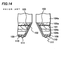
- Fig. 14 shows a cross-sectional view of the BGA type semiconductor devices 100 divided along dicing lines into individual dice.
- the first wiring 103 is provided on an insulation film 102 on a top surface of the semiconductor die 101.
- the semiconductor die 101 is bonded to the first glass substrate 104a with the resin 105a.
- a back surface of the semiconductor die 101 is bonded to the second glass substrate 104b with the resin 105b.
- One end of the first wiring 103 is connected to the second wiring 109.
- the second wiring 109 extends from the end of the first wiring 103 to a surface of the second glass substrate 104b.
- the ball-shaped conductive terminal 111 is formed on the second wiring 109 extending onto the second glass substrate 104b.
- the semiconductor device described above has disadvantages of increased thickness and higher manufacturing cost, since it uses two glass substrates. So, a method to bond the glass substrate only to the top surface of the semiconductor die, on which the first wiring is formed, has been considered. In this case, the bottom surface of the device is made of the semiconductor substrate which is easier to process by etching compared with the glass substrate. Taking this advantage, the first wiring is exposed by etching the semiconductor substrate and the insulation film in the dicing line region in order for the first wiring to be connected with the second wiring. As a result, a contact area between the first wiring and the second wiring is increased, compared with the conventional method using two glass substrates. After forming the second wirings, a protection film and the conductive terminals, the semiconductor substrate is finally separated into individual semiconductor dice by cutting the glass substrate.
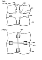
- the insulation film formed on the semiconductor substrate is left exposed in the dicing line region after the first wiring is exposed. At that time, only the insulation film, the resin and the glass substrate exist in the dicing line region. Considering thickness of each component, all of the semiconductor dice are supported practically only with the glass substrate. Furthermore, considerable warping is caused in the glass substrate, because of the difference in thermal expansion coefficients between the semiconductor substrate and the glass substrate. Therefore, weights of the semiconductor dice and others bonded to the glass substrate are imposed on the glass substrate during handling in the manufacturing process. In some cases, this may cause separation 204 between the semiconductor die and the glass substrate (not shown) in peripheral regions of the semiconductor dice and cracks 205 in the glass substrate 202, as shown in Fig. 11. Thus, the yield and reliability of the semiconductor devices have been reduced.
- the invention provides a method of manufacturing a semiconductor device.
- the method includes providing a semiconductor substrate having a plurality of semiconductor dice, a boundary region between two of the semiconductor dice, an insulation film formed on a surface of the semiconductor substrate to cover at least the boundary region, and a pair of wirings formed on the insulation film so that the a center of the boundary region is located between the pair of wirings.
- the method also includes bonding a supporting body to the surface of the semiconductor substrate to cover the pair of wirings, and forming an opening in the semiconductor substrate so as to expose the insulation film between the pair of wirings and to expose at least part of the insulation film that is under the pair of wirings.
- the invention further provides a semiconductor device intermediate.
- the invention achieves to maintain the area of the semiconductor substrate that is bonded to the supporting body large by forming the opening only in the regions around the first wiring. This has the advantage that the bonding strength between the semiconductor substrate and the supporting body is stronger than it was achievable by using a conventional method. Further, warping of the supporting body due to a difference in thermal expansion coefficient between the semiconductor substrate and the supporting body is reduced. For the same token, a risk of developing cracks or separation of the semiconductor device is reduced.
- the invention provides for an improved dicing. It is performed in two steps, the groove is formed first and dicing is made only after a protection film is formed to cover the groove.
- a semiconductor substrate 1 is provided, as shown in Fig. 1.
- CCD image sensors or semiconductor memories are formed in the semiconductor substrate 1 through semiconductor wafer processing.
- a pair of first wirings 3 separated by a predetermined spacing is formed on a surface of the semiconductor substrate 1 through a first insulation film 2 around a border (also referred to as a dicing line or a scribe line) S to divide the semiconductor substrate 1 into individual semiconductor dice.
- Each of the pair of first wirings 3 makes a pad extending from a bonding pad in the semiconductor device to proximity of the border S. That is, each of the pair of first wirings 3 is a pad for external connection, and is electrically connected with a circuit (not shown) in the semiconductor device.
- a glass substrate 4 is provided as a supporting body and is bonded to a surface of the semiconductor substrate 1 on which the first wirings 3 are formed, using a transparent resin 5 (an epoxy resin, for example) as an adhesive.
- a transparent resin 5 an epoxy resin, for example
- a silicon substrate or a plastic plate may be used as the supporting body other than the glass substrate used in the embodiment.
- An adhesive suitable for the chosen supporting body is to be selected in this case.
- Thickness of the semiconductor substrate 1 is reduced by back-grinding a surface of the semiconductor substrate 1, which is opposite from the surface facing the glass substrate 4. Scratches arise on the back-ground surface of the semiconductor substrate 1, causing bumps and dips of several micrometers in width and in depth.
- the back-ground surface is wet-etched using a chemical solution having a high selection ratio between an etching rate for silicon which is a material of the semiconductor substrate 1 and an etching rate for silicon oxide which is a material of the first insulation film 2.
- the chemical solution there is no specific restriction on the chemical solution as long as it has a high selection ratio.
- a mixed solution composed of 2.5% of hydrofluoric acid, 50% of nitric acid, 10% of acetic acid and 37.5% of water is used as the etching solution in this embodiment.
- this invention does not necessarily include the wet-etching.
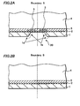
- the semiconductor substrate 1 is etched isotropically (or anisotropically) to expose portions of the first wirings 3, using a mask of photoresist (not shown) formed on the surface of the semiconductor substrate 1 opposite from the surface facing the glass substrate 4, as shown in Figs. 2A and 2B.
- a window 20 opened along a border S in a region around the first wirings 3 is formed to expose the first insulation film 2, as shown in Fig. 2A.
- the semiconductor substrate 1 remains intact in a region where the first wiring does not exist, as shown in Fig. 2B.
- the area of the semiconductor substrate 1 bonded to the glass substrate 4 through the first insulation film 2 and the resin 5 is still maintained large by forming the windows 20 which are opened only in the regions around the first wirings 3, as described above.
- Strength to support the glass substrate 4 is stronger than the conventional method. Also, warping of the glass substrate 4 due to the difference in thermal expansion coefficients between the semiconductor substrate 1 and the glass substrate 4 is reduced as well as cracks and separation in the semiconductor device.
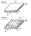
- Fig. 12 shows a plan view of the device intermediate at the process step of Figs. 2A and 2B. Only a portion of a semiconductor substrate in the region under and between the pair of first wirings 301 is removed by etching instead of the whole scribe line region 304. The portion removed by the etching is called a window 303, which corresponds to the window 20 shown in Fig. 2A. As a result, most area of a supporting body is in contact with the semiconductor substrate 302 through the resin and the insulation film.
- etching may be performed either by dry-etching or by wet-etching.
- symbol A denotes a figure showing the region where the window 20 is formed
- symbol B denotes a figure showing the region where the window 20 is not formed, as in the case of Fig. 2A and Fig. 2B.
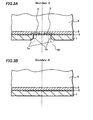
- a second insulation film 6 is formed on the surface of the semiconductor substrate 1 opposite from the surface facing the glass substrate 4, as shown in Figs. 4A and 4B.
- a silane-based oxide film of 3 ⁇ m in thickness is formed in this embodiment.
- a photoresist film (not shown) is applied above the surface of the semiconductor substrate 1 opposite from the surface facing the glass substrate 4 and pattering is made to form an opening in the photoresist film in the window 20 along the border S.
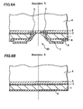
- portions of the first wirings 3 are exposed by etching the second insulation film 6 and the first insulation film 2 using the photoresist film (not shown) as a mask, as shown in Figs. 5A and 5B.
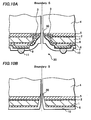
- flexible cushioning pads 7 are formed at locations where conductive terminals 11 are formed later, as shown in Figs. 6A and 6B.
- the cushioning pads 7 have function to absorb power applied through the conductive terminals 11 and relax stress when the conductive terminals 11 are bonded.
- this invention does not necessarily require including the cushioning pads 7.
- a second wiring layer 8 is formed above the surface of the semiconductor substrate 1 opposite from the surface facing the glass substrate 4. With this, each of the first wirings 3 is electrically connected with the second wiring layer 8.
- a photoresist film (not shown) is applied above the surface of the semiconductor substrate 1 opposite from the surface facing the glass substrate 4. An opening is formed in the photoresist film in the window 20 along the border S in the region where the window 20 has been formed.
- the photoresist film is removed to expose the second wiring layer 8 in the region where the window 20 is not formed. Etching is performed using the photoresist film (not shown) as a mask to remove a portion of the second wiring layer 8 around the border S. Also, the second wiring layer 8 in the region where the window 20 is not formed is removed to complete the second wirings 8.
- a slit 30 (an inverted V-shaped groove) is formed in the glass substrate 4 along the border S so that the glass substrate 4 is cut to a depth of 30 ⁇ m, for example, as shown in Figs. 7A and 7B.
- the resin 5 and a portion of the glass substrate 4 are cut to form the slit 30 in the region where the first wirings 3 exist (the region in the window 20 along the border S). It is necessary to use a blade of a width narrow enough not to contact the second wirings 8 in the window 20 in this process.
- the semiconductor substrate 1, the first insulation film 2, the resin 5 and a portion of the glass substrate 4 are cut to form the slit 30 in the region where the first wiring 3 does not exist (i. e., the region where the window 20 is not formed).
- the slit 30 has a wedge-shaped cross-section in the embodiment, it may have a rectangular cross-section. Besides, this invention does not necessary require the process step to form the slit 30.
- electroless plating is applied to the surface above the semiconductor substrate 1 opposite from the surface facing the glass substrate 4 to form a Ni-Au plating film 9 on the second wirings 8, as shown in Figs. 8A and 8B.
- the film is formed only on the second wirings 8 because it is formed by plating.
- a protection film 10 is formed on a surface above the semiconductor substrate 1 opposite from the surface facing the glass substrate 4, as shown in Figs. 9A and 9B.
- the surface opposite from the surface facing the glass substrate 4 is held upward, a thermosetting organic resin is dropped on it and the organic resin is spread over the surface by spinning the semiconductor substrate 1 utilizing centrifugal force.
- the protection film 10 is formed above the back surface of the semiconductor substrate 1 including a inner wall of the slit 30 formed along the border S.
- the protection film 10 is formed to cover the second insulation film 6 and the resin 5 and the glass substrate 4 exposed on the inner wall of the slit 30 in the region where the first wirings 3 exist (the region in the window 20 along the border S).
- the protection film 10 is formed to cover the second insulation film 6, the semiconductor substrate 1, the first insulation film 2, the resin 5 and the glass substrate 4 exposed on the inner wall of the slit 30 in the region other than the region where the first wirings 3 exist (i. e. the region where the window 20 is not formed).
- portions of the protection film 10 above locations where the conductive terminals 11 are to be formed are removed by etching using a photoresist film (with openings at locations corresponding to the cushioning pads 7, not shown) as a mask and the conductive terminals 11 are formed on the Ni-Au plating film 9 at the locations corresponding to the cushioning pads 7.
- the conductive terminals 11 are electrically connected with the second wirings 8 through the Ni-Au plating film 9.
- the conductive terminals 11 are formed of solder bumps of gold bumps. When the gold bumps are used, thickness of the conductive terminal 11 can be reduced from 160 ⁇ m to several micrometers or several tens of micrometers.
- a dicing blade preferably has a width to cut only the glass substrate 4 and the protection film 10 in the slit 30.
- the dicing is performed in two steps, that is, the slit 30 is formed and then dicing is made after forming the protection film 10 to cover the slit 30.
- separation can be made by dicing only the glass substrate 4 and the protection film 10, since the inner wall of the slit 30 formed along the border S (i. e. the dicing line) is covered with the protection film 10 when the dicing to separate the semiconductor device into the individual dice is performed.
- the blade does not contact layers (the resin 5, the second wirings 8, etc.) and contacts only the glass substrate 4 and the protection film 10. Therefore, the separation caused in the separated semiconductor device, that is, on a cut surface or at an edge of the semiconductor dice by contacting the blade in the dicing process, can be prevented as much as possible.
- the semiconductor device of this invention can be made thinner and produced at reduced cost, since it is formed of the single glass substrate.
- this invention does not necessarily require the terminals. That is, this invention may be applied to a semiconductor device without the conductive terminals (an LGA (Land Grid Array) type package, for example).
- LGA Land Grid Array
- Yield and reliability can be improved by preventing the cracks caused in the glass substrate and the separation in the peripheral regions of the semiconductor dice with this invention.
- the semiconductor device can be made thinner and produced at reduced cost, since a number of the glass substrates used in the device is reduced from two to one.
Abstract
Description
- This invention relates to a semiconductor device and manufacturing method thereof, specifically to a semiconductor device encapsulated in a package having roughly the same outside dimensions as a semiconductor die packaged in it and a manufacturing method thereof.
- A CSP (Chip Size Package) has received attention in recent years as a new packaging technology. The CSP means a small package having about the same outside dimensions as those of a semiconductor die packaged in it. A BGA type semiconductor device has been known as a kind of CSP. A plurality of ball-shaped conductive terminals made of metal such as solder is arrayed in a grid pattern on one principal surface of a package of the BGA type semiconductor device and is electrically connected with the semiconductor die mounted on the other side of the package.
- When the BGA type semiconductor device is mounted on electronic equipment, the semiconductor die is electrically connected with an external circuit on a printed circuit board by compression bonding of the conductive terminals to wiring patterns on the printed circuit board.
- Such a BGA type semiconductor device has advantages in providing a large number of conductive terminals and in reducing size over other CSP type semiconductor devices such as an SOP (Small Outline Package) and a QFP (Quad Flat Package), which have lead pins protruding from their sides. The BGA type semiconductor device is used as an image sensor chip for a digital camera incorporated into a mobile telephone, for example.
- Figs. 13A and 13B show outline structure of a conventional BGA type semiconductor device. Fig. 13A is an oblique perspective figure showing a top side of the BGA type semiconductor device. And Fig. 13B is an oblique perspective figure showing a back side of the BGA type semiconductor device.
- A
semiconductor die 101 is sealed between afirst glass substrate 104a and asecond glass substrate 104b throughresins type semiconductor device 100. A plurality of ball-shaped conductive terminals (hereafter referred to as conductive terminals) 111 is arrayed in a grid pattern on a principal surface of thesecond glass substrate 104b, that is, on a back surface of the BGAtype semiconductor device 100. Theconductive terminals 111 are connected to the semiconductor die 101 through a plurality ofsecond wirings 109. The plurality ofsecond wirings 109 is connected with aluminum first wirings pulled out from inside of thesemiconductor die 101, making each of theconductive terminals 111 electrically connected with thesemiconductor die 101. - More detailed explanation on a cross-sectional structure of the BGA
type semiconductor device 100 is given hereafter referring to Fig. 14. Fig. 14 shows a cross-sectional view of the BGAtype semiconductor devices 100 divided along dicing lines into individual dice. - The
first wiring 103 is provided on aninsulation film 102 on a top surface of the semiconductor die 101. Thesemiconductor die 101 is bonded to thefirst glass substrate 104a with theresin 105a. A back surface of thesemiconductor die 101 is bonded to thesecond glass substrate 104b with theresin 105b. One end of thefirst wiring 103 is connected to thesecond wiring 109. Thesecond wiring 109 extends from the end of thefirst wiring 103 to a surface of thesecond glass substrate 104b. The ball-shapedconductive terminal 111 is formed on thesecond wiring 109 extending onto thesecond glass substrate 104b. - The semiconductor device described above has disadvantages of increased thickness and higher manufacturing cost, since it uses two glass substrates. So, a method to bond the glass substrate only to the top surface of the semiconductor die, on which the first wiring is formed, has been considered. In this case, the bottom surface of the device is made of the semiconductor substrate which is easier to process by etching compared with the glass substrate. Taking this advantage, the first wiring is exposed by etching the semiconductor substrate and the insulation film in the dicing line region in order for the first wiring to be connected with the second wiring. As a result, a contact area between the first wiring and the second wiring is increased, compared with the conventional method using two glass substrates. After forming the second wirings, a protection film and the conductive terminals, the semiconductor substrate is finally separated into individual semiconductor dice by cutting the glass substrate.
- The insulation film formed on the semiconductor substrate is left exposed in the dicing line region after the first wiring is exposed. At that time, only the insulation film, the resin and the glass substrate exist in the dicing line region. Considering thickness of each component, all of the semiconductor dice are supported practically only with the glass substrate. Furthermore, considerable warping is caused in the glass substrate, because of the difference in thermal expansion coefficients between the semiconductor substrate and the glass substrate. Therefore, weights of the semiconductor dice and others bonded to the glass substrate are imposed on the glass substrate during handling in the manufacturing process. In some cases, this may cause
separation 204 between the semiconductor die and the glass substrate (not shown) in peripheral regions of the semiconductor dice andcracks 205 in theglass substrate 202, as shown in Fig. 11. Thus, the yield and reliability of the semiconductor devices have been reduced. - It is an object of this invention to provide a manufacturing method that lessens this drawback.
- The solution according to the invention lies in the features of the independent claims and preferably in those of the dependent claims.
- The invention provides a method of manufacturing a semiconductor device. The method includes providing a semiconductor substrate having a plurality of semiconductor dice, a boundary region between two of the semiconductor dice, an insulation film formed on a surface of the semiconductor substrate to cover at least the boundary region, and a pair of wirings formed on the insulation film so that the a center of the boundary region is located between the pair of wirings. The method also includes bonding a supporting body to the surface of the semiconductor substrate to cover the pair of wirings, and forming an opening in the semiconductor substrate so as to expose the insulation film between the pair of wirings and to expose at least part of the insulation film that is under the pair of wirings.
- The invention further provides a semiconductor device intermediate. The invention achieves to maintain the area of the semiconductor substrate that is bonded to the supporting body large by forming the opening only in the regions around the first wiring. This has the advantage that the bonding strength between the semiconductor substrate and the supporting body is stronger than it was achievable by using a conventional method. Further, warping of the supporting body due to a difference in thermal expansion coefficient between the semiconductor substrate and the supporting body is reduced. For the same token, a risk of developing cracks or separation of the semiconductor device is reduced. Moreover, the invention provides for an improved dicing. It is performed in two steps, the groove is formed first and dicing is made only after a protection film is formed to cover the groove. Doing so has the advantage that separation can be made by dicing only the supporting body and the protection film as the inner wall of the groove formed along the dicing line is covered with a protection film, thus avoiding contact of the means used for dicing with wiring layers of the semiconductor substrate.
-
- Fig. 1 is a cross-sectional view showing a manufacturing method of a semiconductor device according to an embodiment of this invention.
- Figs. 2A and 2B are cross-sectional views showing the manufacturing method of the semiconductor device according to the embodiment of this invention.
- Figs. 3A and 3B are cross-sectional views showing the manufacturing method of the semiconductor device according to the embodiment of this invention.
- Figs. 4A and 4B are cross-sectional views showing the manufacturing method of the semiconductor device according to the embodiment of this invention.
- Figs. 5A and 5B are cross-sectional views showing the manufacturing method of the semiconductor device according to the embodiment of this invention.
- Figs. 6A and 6B are cross-sectional views showing the manufacturing method of the semiconductor device according to the embodiment of this invention.
- Figs. 7A and 7B are cross-sectional views showing the manufacturing method of the semiconductor device according to the embodiment of this invention.
- Figs. 8A and 8B are cross-sectional views showing the manufacturing method of the semiconductor device according to the embodiment of this invention.
- Figs. 9A and 9B are cross-sectional views showing the manufacturing method of the semiconductor device according to the embodiment of this invention.
- Figs. 10A and 10B are cross-sectional views showing the manufacturing method of the semiconductor device according to the embodiment of this invention.
- Fig. 11 is a plan view showing a BGA type semiconductor device intermediate according to conventional art.
- Fig. 12 is a plan view showing the semiconductor device intermediate according to the embodiment of this invention.
- Figs. 13A and 13B are oblique perspective views showing the BGA type semiconductor device according to the conventional art.
- Fig. 14 is a cross-sectional view showing the BGA type semiconductor device according to the conventional art.
-
- Next, a manufacturing method of a semiconductor device according to an embodiment of this invention will be described referring to cross-sectional views shown in Fig. 1 through Fig. 10 and a plan view shown in Fig. 12 of the semiconductor device.
- First, a
semiconductor substrate 1 is provided, as shown in Fig. 1. CCD image sensors or semiconductor memories, for example, are formed in thesemiconductor substrate 1 through semiconductor wafer processing. A pair offirst wirings 3 separated by a predetermined spacing is formed on a surface of thesemiconductor substrate 1 through afirst insulation film 2 around a border (also referred to as a dicing line or a scribe line) S to divide thesemiconductor substrate 1 into individual semiconductor dice. Each of the pair offirst wirings 3 makes a pad extending from a bonding pad in the semiconductor device to proximity of the border S. That is, each of the pair offirst wirings 3 is a pad for external connection, and is electrically connected with a circuit (not shown) in the semiconductor device. - Next, a
glass substrate 4 is provided as a supporting body and is bonded to a surface of thesemiconductor substrate 1 on which thefirst wirings 3 are formed, using a transparent resin 5 (an epoxy resin, for example) as an adhesive. Note that a silicon substrate or a plastic plate may be used as the supporting body other than the glass substrate used in the embodiment. An adhesive suitable for the chosen supporting body is to be selected in this case. - Thickness of the
semiconductor substrate 1 is reduced by back-grinding a surface of thesemiconductor substrate 1, which is opposite from the surface facing theglass substrate 4. Scratches arise on the back-ground surface of thesemiconductor substrate 1, causing bumps and dips of several micrometers in width and in depth. In order to reduce the bumps and dips, the back-ground surface is wet-etched using a chemical solution having a high selection ratio between an etching rate for silicon which is a material of thesemiconductor substrate 1 and an etching rate for silicon oxide which is a material of thefirst insulation film 2. - There is no specific restriction on the chemical solution as long as it has a high selection ratio. For example, a mixed solution composed of 2.5% of hydrofluoric acid, 50% of nitric acid, 10% of acetic acid and 37.5% of water is used as the etching solution in this embodiment.
- Although doing the wet-etching is preferable, this invention does not necessarily include the wet-etching.
- Next, the
semiconductor substrate 1 is etched isotropically (or anisotropically) to expose portions of thefirst wirings 3, using a mask of photoresist (not shown) formed on the surface of thesemiconductor substrate 1 opposite from the surface facing theglass substrate 4, as shown in Figs. 2A and 2B. As a result, awindow 20 opened along a border S in a region around thefirst wirings 3 is formed to expose thefirst insulation film 2, as shown in Fig. 2A. On the other hand, thesemiconductor substrate 1 remains intact in a region where the first wiring does not exist, as shown in Fig. 2B. - The area of the
semiconductor substrate 1 bonded to theglass substrate 4 through thefirst insulation film 2 and theresin 5 is still maintained large by forming thewindows 20 which are opened only in the regions around thefirst wirings 3, as described above. Strength to support theglass substrate 4 is stronger than the conventional method. Also, warping of theglass substrate 4 due to the difference in thermal expansion coefficients between thesemiconductor substrate 1 and theglass substrate 4 is reduced as well as cracks and separation in the semiconductor device. - Fig. 12 shows a plan view of the device intermediate at the process step of Figs. 2A and 2B. Only a portion of a semiconductor substrate in the region under and between the pair of
first wirings 301 is removed by etching instead of the wholescribe line region 304. The portion removed by the etching is called awindow 303, which corresponds to thewindow 20 shown in Fig. 2A. As a result, most area of a supporting body is in contact with thesemiconductor substrate 302 through the resin and the insulation film. - Note that the etching may be performed either by dry-etching or by wet-etching. In explanations on the manufacturing process hereafter, symbol A denotes a figure showing the region where the
window 20 is formed, while symbol B denotes a figure showing the region where thewindow 20 is not formed, as in the case of Fig. 2A and Fig. 2B. - There are bumps and dips, residues and foreign particles on the surface of the
semiconductor substrate 1. In addition, there are sharp edges at corners of thewindow 20, as shown in circles denoted 1a and 1b in Fig. 2A. - Wet-etching is made to remove the residues and the foreign particles and round the sharp edges, as shown in Figs. 3A and 3B. With this, the sharp edges shown in the
circles circles - Next, a
second insulation film 6 is formed on the surface of thesemiconductor substrate 1 opposite from the surface facing theglass substrate 4, as shown in Figs. 4A and 4B. A silane-based oxide film of 3 µm in thickness is formed in this embodiment. - Next, a photoresist film (not shown) is applied above the surface of the
semiconductor substrate 1 opposite from the surface facing theglass substrate 4 and pattering is made to form an opening in the photoresist film in thewindow 20 along the border S. Then portions of thefirst wirings 3 are exposed by etching thesecond insulation film 6 and thefirst insulation film 2 using the photoresist film (not shown) as a mask, as shown in Figs. 5A and 5B. - Next,
flexible cushioning pads 7 are formed at locations whereconductive terminals 11 are formed later, as shown in Figs. 6A and 6B. Thecushioning pads 7 have function to absorb power applied through theconductive terminals 11 and relax stress when theconductive terminals 11 are bonded. However, this invention does not necessarily require including thecushioning pads 7. - A
second wiring layer 8 is formed above the surface of thesemiconductor substrate 1 opposite from the surface facing theglass substrate 4. With this, each of thefirst wirings 3 is electrically connected with thesecond wiring layer 8. - After that, a photoresist film (not shown) is applied above the surface of the
semiconductor substrate 1 opposite from the surface facing theglass substrate 4. An opening is formed in the photoresist film in thewindow 20 along the border S in the region where thewindow 20 has been formed. On the other hand, the photoresist film is removed to expose thesecond wiring layer 8 in the region where thewindow 20 is not formed. Etching is performed using the photoresist film (not shown) as a mask to remove a portion of thesecond wiring layer 8 around the border S. Also, thesecond wiring layer 8 in the region where thewindow 20 is not formed is removed to complete thesecond wirings 8. - Next, a slit 30 (an inverted V-shaped groove) is formed in the
glass substrate 4 along the border S so that theglass substrate 4 is cut to a depth of 30 µm, for example, as shown in Figs. 7A and 7B. - That is, the
resin 5 and a portion of theglass substrate 4 are cut to form theslit 30 in the region where thefirst wirings 3 exist (the region in thewindow 20 along the border S). It is necessary to use a blade of a width narrow enough not to contact thesecond wirings 8 in thewindow 20 in this process. - On the other hand, the
semiconductor substrate 1, thefirst insulation film 2, theresin 5 and a portion of theglass substrate 4 are cut to form theslit 30 in the region where thefirst wiring 3 does not exist (i. e., the region where thewindow 20 is not formed). - Although the
slit 30 has a wedge-shaped cross-section in the embodiment, it may have a rectangular cross-section. Besides, this invention does not necessary require the process step to form theslit 30. - Next, electroless plating is applied to the surface above the
semiconductor substrate 1 opposite from the surface facing theglass substrate 4 to form a Ni-Au plating film 9 on thesecond wirings 8, as shown in Figs. 8A and 8B. The film is formed only on thesecond wirings 8 because it is formed by plating. - Next, a
protection film 10 is formed on a surface above thesemiconductor substrate 1 opposite from the surface facing theglass substrate 4, as shown in Figs. 9A and 9B. In order to form theprotection film 10, the surface opposite from the surface facing theglass substrate 4 is held upward, a thermosetting organic resin is dropped on it and the organic resin is spread over the surface by spinning thesemiconductor substrate 1 utilizing centrifugal force. With this, theprotection film 10 is formed above the back surface of thesemiconductor substrate 1 including a inner wall of theslit 30 formed along the border S. - In other words, the
protection film 10 is formed to cover thesecond insulation film 6 and theresin 5 and theglass substrate 4 exposed on the inner wall of theslit 30 in the region where thefirst wirings 3 exist (the region in thewindow 20 along the border S). On the other hand, theprotection film 10 is formed to cover thesecond insulation film 6, thesemiconductor substrate 1, thefirst insulation film 2, theresin 5 and theglass substrate 4 exposed on the inner wall of theslit 30 in the region other than the region where thefirst wirings 3 exist (i. e. the region where thewindow 20 is not formed). - After that, portions of the
protection film 10 above locations where theconductive terminals 11 are to be formed are removed by etching using a photoresist film (with openings at locations corresponding to thecushioning pads 7, not shown) as a mask and theconductive terminals 11 are formed on the Ni-Au plating film 9 at the locations corresponding to thecushioning pads 7. Theconductive terminals 11 are electrically connected with thesecond wirings 8 through the Ni-Au plating film 9. Theconductive terminals 11 are formed of solder bumps of gold bumps. When the gold bumps are used, thickness of theconductive terminal 11 can be reduced from 160 µm to several micrometers or several tens of micrometers. - Then the semiconductor substrate is diced into individual semiconductor dice along the border S at a portion where the
slit 30 is provided, as shown in Figs. 10A and 10B. A dicing blade preferably has a width to cut only theglass substrate 4 and theprotection film 10 in theslit 30. - In the manufacturing method of the semiconductor device according to the embodiment, the dicing is performed in two steps, that is, the
slit 30 is formed and then dicing is made after forming theprotection film 10 to cover theslit 30. By doing so, separation can be made by dicing only theglass substrate 4 and theprotection film 10, since the inner wall of theslit 30 formed along the border S (i. e. the dicing line) is covered with theprotection film 10 when the dicing to separate the semiconductor device into the individual dice is performed. It means that the blade does not contact layers (theresin 5, thesecond wirings 8, etc.) and contacts only theglass substrate 4 and theprotection film 10. Therefore, the separation caused in the separated semiconductor device, that is, on a cut surface or at an edge of the semiconductor dice by contacting the blade in the dicing process, can be prevented as much as possible. - As a result, yield and reliability of the semiconductor device can be improved. Also, the semiconductor device of this invention can be made thinner and produced at reduced cost, since it is formed of the single glass substrate.
- Although the
conductive terminals 11 electrically connected with thesecond wirings 8 are formed in this embodiment, this invention does not necessarily require the terminals. That is, this invention may be applied to a semiconductor device without the conductive terminals (an LGA (Land Grid Array) type package, for example). - Yield and reliability can be improved by preventing the cracks caused in the glass substrate and the separation in the peripheral regions of the semiconductor dice with this invention. In addition, the semiconductor device can be made thinner and produced at reduced cost, since a number of the glass substrates used in the device is reduced from two to one.
Claims (8)
- A method of manufacturing a semiconductor device, comprising:providing a semiconductor substrate (1) comprising a plurality of semiconductor dice, a boundary region between two of the semiconductor dice, an insulation film (2) formed on a surface of the semiconductor substrate (1) to cover at least the boundary region, and a pair of wirings (3) formed on the insulation film (2) so that the a center of the boundary region is located between the pair of wirings (3);bonding a supporting body (4) to the surface of the semiconductor substrate (1) to cover the pair of wirings (3); andforming an opening (20) in the semiconductor substrate (1) so as to expose the insulation film (2) between the pair of wirings (3) and to expose at least part of the insulation film (2) that is under the pair of wirings (3).
- A method of manufacturing a semiconductor device, comprising:providing a semiconductor substrate (1) comprising a plurality of semiconductor dice, a boundary region between two of the semiconductor dice, a first insulation film (2) formed on a first surface of the semiconductor substrate (1) to cover at least the boundary region, and a pair of first wirings (3) formed on the first insulation film (2) so that the a center of the boundary region is located between the pair of first wirings (3);bonding a supporting body (4) to the first surface of the semiconductor substrate (1) to cover the pair of first wirings (3);removing part of the semiconductor substrate (1) to expose part of the first insulation film (3) from a second surface of the semiconductor substrate (1);forming a second insulation film (6) on the second surface of the semiconductor substrate (1);selectively etching the first insulation film (2) and the second insulation film (6) to expose at least portions of the pair of first wirings (3);forming a second wiring (8) on the second surface of the semiconductor substrate (1) so that the second wiring (8) is connected to the pair of first wirings (3);forming a groove (30) in the second surface of the semiconductor substrate (1) along the boundary region; anddicing the semiconductor substrate (1) and the supporting body (4) along the groove (30) to separate the semiconductor substrate (1) into individual semiconductor dice.
- The method of claim 2, wherein a width of a region of the semiconductor substrate (1) removed by the dicing is narrower than a spacing between the pair of first wirings (3).
- The method of claim 2 or 3, wherein the forming of the groove (30) is such that the groove (30) reaches the supporting body (4).
- The method according to any of claims 2 to 4, further comprising covering the groove (30) with a protection film (10), wherein only the protection film (10) and the supporting body (4) are removed by the dicing.
- A semiconductor device intermediate comprising:a semiconductor substrate (1) having an insulation film (2) formed on a first surface thereof;a pair of first wirings (3) formed on the insulation film (2) so that a dicing line is located between the pair of first wirings (3);a supporting body (4) disposed on the insulation film (2) and the pair of first wirings (3);an adhesive layer (5) attaching the supporting body (4) to the insulation film (2) and the pair of first wirings (3);an opening (20) formed from a second surface of the semiconductor substrate (1) to expose the adhesive layer (5) between the pair of first wiring (3); anda pair of second wirings (8) each connected to corresponding one of the pair of first wirings (3) through the opening (20).
- The semiconductor device intermediate of claim 6, further comprising a groove (30) made in the adhesive layer (5) between the pair of first wirings (3) and reaching the supporting body (4).
- The semiconductor device intermediate of claim 7, further comprising a protection film (10) covering the groove (30).
Applications Claiming Priority (4)
| Application Number | Priority Date | Filing Date | Title |
|---|---|---|---|
| JP2003288150 | 2003-08-06 | ||
| JP2003288150 | 2003-08-06 | ||
| JP2004022989 | 2004-01-30 | ||
| JP2004022989A JP4401181B2 (en) | 2003-08-06 | 2004-01-30 | Semiconductor device and manufacturing method thereof |
Publications (3)
| Publication Number | Publication Date |
|---|---|
| EP1505643A2 true EP1505643A2 (en) | 2005-02-09 |
| EP1505643A3 EP1505643A3 (en) | 2009-05-06 |
| EP1505643B1 EP1505643B1 (en) | 2012-11-14 |
Family
ID=33554530
Family Applications (1)
| Application Number | Title | Priority Date | Filing Date |
|---|---|---|---|
| EP04018715A Expired - Fee Related EP1505643B1 (en) | 2003-08-06 | 2004-08-06 | Semiconductor device and manufacturing method thereof |
Country Status (6)
| Country | Link |
|---|---|
| US (2) | US7312107B2 (en) |
| EP (1) | EP1505643B1 (en) |
| JP (1) | JP4401181B2 (en) |
| KR (1) | KR100636770B1 (en) |
| CN (1) | CN100367451C (en) |
| TW (1) | TWI236046B (en) |
Cited By (1)
| Publication number | Priority date | Publication date | Assignee | Title |
|---|---|---|---|---|
| CN100440495C (en) * | 2005-03-29 | 2008-12-03 | 三洋电机株式会社 | Semiconductor device and manufacturing method thereof |
Families Citing this family (45)
| Publication number | Priority date | Publication date | Assignee | Title |
|---|---|---|---|---|
| TWI232560B (en) | 2002-04-23 | 2005-05-11 | Sanyo Electric Co | Semiconductor device and its manufacture |
| TWI229435B (en) * | 2002-06-18 | 2005-03-11 | Sanyo Electric Co | Manufacture of semiconductor device |
| TWI227550B (en) | 2002-10-30 | 2005-02-01 | Sanyo Electric Co | Semiconductor device manufacturing method |
| JP4401181B2 (en) | 2003-08-06 | 2010-01-20 | 三洋電機株式会社 | Semiconductor device and manufacturing method thereof |
| JP4322181B2 (en) * | 2004-07-29 | 2009-08-26 | 三洋電機株式会社 | Manufacturing method of semiconductor device |
| KR100604903B1 (en) * | 2004-09-30 | 2006-07-28 | 삼성전자주식회사 | Semiconductor wafer with improved step coverage and fabrication method of the same |
| US7772038B2 (en) * | 2005-09-30 | 2010-08-10 | Retro Reflective Optics, Llc | CMOS process for fabrication of ultra small or non standard size or shape semiconductor die |
| JP2007165696A (en) | 2005-12-15 | 2007-06-28 | Sanyo Electric Co Ltd | Semiconductor device, and process for fabrication thereof |
| JP5010244B2 (en) | 2005-12-15 | 2012-08-29 | オンセミコンダクター・トレーディング・リミテッド | Semiconductor device |
| TWI324800B (en) | 2005-12-28 | 2010-05-11 | Sanyo Electric Co | Method for manufacturing semiconductor device |
| TW200737506A (en) | 2006-03-07 | 2007-10-01 | Sanyo Electric Co | Semiconductor device and manufacturing method of the same |
| JP2008003577A (en) * | 2006-05-25 | 2008-01-10 | Canon Inc | Method of manufacturing image display device and method of dividing device |
| TWI367557B (en) | 2006-08-11 | 2012-07-01 | Sanyo Electric Co | Semiconductor device and manufaturing method thereof |
| US9034729B2 (en) | 2006-08-25 | 2015-05-19 | Semiconductor Components Industries, Llc | Semiconductor device and method of manufacturing the same |
| WO2008023827A1 (en) | 2006-08-25 | 2008-02-28 | Sanyo Electric Co., Ltd. | Semiconductor device |
| US8148811B2 (en) | 2006-08-25 | 2012-04-03 | Semiconductor Components Industries, Llc | Semiconductor device and manufacturing method thereof |
| US8513789B2 (en) * | 2006-10-10 | 2013-08-20 | Tessera, Inc. | Edge connect wafer level stacking with leads extending along edges |
| US7901989B2 (en) | 2006-10-10 | 2011-03-08 | Tessera, Inc. | Reconstituted wafer level stacking |
| JP4743631B2 (en) | 2006-10-23 | 2011-08-10 | 三洋電機株式会社 | Semiconductor device and manufacturing method thereof |
| JP5010247B2 (en) | 2006-11-20 | 2012-08-29 | オンセミコンダクター・トレーディング・リミテッド | Semiconductor device and manufacturing method thereof |
| US7569409B2 (en) * | 2007-01-04 | 2009-08-04 | Visera Technologies Company Limited | Isolation structures for CMOS image sensor chip scale packages |
| JP5301108B2 (en) | 2007-04-20 | 2013-09-25 | セミコンダクター・コンポーネンツ・インダストリーズ・リミテッド・ライアビリティ・カンパニー | Semiconductor device |
| JP2008294405A (en) | 2007-04-25 | 2008-12-04 | Sanyo Electric Co Ltd | Semiconductor device, and method of manufacturing the same |
| JP5572089B2 (en) | 2007-07-27 | 2014-08-13 | テッセラ,インコーポレイテッド | Reconfigured wafer stack packaging with pad extension after application |
| JP2009032929A (en) | 2007-07-27 | 2009-02-12 | Sanyo Electric Co Ltd | Semiconductor device and method of manufacturing the same |
| KR100887479B1 (en) * | 2007-10-09 | 2009-03-10 | 주식회사 네패스 | Crack resistant semiconduct package and fabrication method thereof |
| JP2010027741A (en) * | 2008-07-16 | 2010-02-04 | Sanyo Electric Co Ltd | Semiconductor device and method of manufacturing same |
| JP2010103300A (en) | 2008-10-23 | 2010-05-06 | Sanyo Electric Co Ltd | Semiconductor device, and method of manufacturing the same |
| DE102008058003B4 (en) * | 2008-11-19 | 2012-04-05 | Infineon Technologies Ag | Method for producing a semiconductor module and semiconductor module |
| JP5985136B2 (en) * | 2009-03-19 | 2016-09-06 | ソニー株式会社 | SEMICONDUCTOR DEVICE, ITS MANUFACTURING METHOD, AND ELECTRONIC DEVICE |
| US8298917B2 (en) * | 2009-04-14 | 2012-10-30 | International Business Machines Corporation | Process for wet singulation using a dicing singulation structure |
| JP5475363B2 (en) * | 2009-08-07 | 2014-04-16 | ラピスセミコンダクタ株式会社 | Semiconductor device and manufacturing method thereof |
| US8952519B2 (en) * | 2010-01-13 | 2015-02-10 | Chia-Sheng Lin | Chip package and fabrication method thereof |
| JP2012028359A (en) * | 2010-07-20 | 2012-02-09 | On Semiconductor Trading Ltd | Semiconductor device and manufacturing method of the same |
| JP5656501B2 (en) * | 2010-08-06 | 2015-01-21 | セミコンダクター・コンポーネンツ・インダストリーズ・リミテッド・ライアビリティ・カンパニー | Semiconductor device and manufacturing method thereof |
| US8722514B2 (en) | 2011-01-17 | 2014-05-13 | Infineon Technologies Ag | Semiconductor devices having insulating substrates and methods of formation thereof |
| DE102011112659B4 (en) * | 2011-09-06 | 2022-01-27 | Vishay Semiconductor Gmbh | Surface mount electronic component |
| JP2013125753A (en) | 2011-12-13 | 2013-06-24 | Semiconductor Components Industries Llc | Semiconductor integrated circuit |
| JP5968711B2 (en) * | 2012-07-25 | 2016-08-10 | ルネサスエレクトロニクス株式会社 | Semiconductor device and manufacturing method of semiconductor device |
| CN102810549B (en) * | 2012-08-29 | 2015-04-01 | 格科微电子(上海)有限公司 | Method for manufacturing wafer-level packages of image sensors |
| TWI525673B (en) * | 2013-10-08 | 2016-03-11 | 精材科技股份有限公司 | Method of fabricating a wafer-level chip package |
| US11244908B2 (en) | 2018-11-06 | 2022-02-08 | STATS ChipPAC Pte. Ltd. | Method and device for reducing metal burrs when sawing semiconductor packages |
| JP2019091945A (en) * | 2019-03-08 | 2019-06-13 | 三星ダイヤモンド工業株式会社 | Manufacturing apparatus of semiconductor chip with solder ball and manufacturing method |
| KR20220006931A (en) | 2020-07-09 | 2022-01-18 | 삼성전자주식회사 | Interposer and semiconductor package including the same |
| US20220102289A1 (en) * | 2020-09-30 | 2022-03-31 | Tokyo Electron Limited | Stress Relief in Semiconductor Wafers |
Citations (2)
| Publication number | Priority date | Publication date | Assignee | Title |
|---|---|---|---|---|
| WO1999040624A1 (en) | 1998-02-06 | 1999-08-12 | Shellcase Ltd. | Integrated circuit device |
| US20030134453A1 (en) | 2002-01-11 | 2003-07-17 | National Semiconductor Corporation | Process and structure improvements to shellcase style packaging technology |
Family Cites Families (122)
| Publication number | Priority date | Publication date | Assignee | Title |
|---|---|---|---|---|
| DE1933731C3 (en) | 1968-07-05 | 1982-03-25 | Honeywell Information Systems Italia S.p.A., Caluso, Torino | Method for producing a semiconductor integrated circuit |
| GB1285708A (en) | 1968-10-28 | 1972-08-16 | Lucas Industries Ltd | Semi-conductor devices |
| US3648131A (en) | 1969-11-07 | 1972-03-07 | Ibm | Hourglass-shaped conductive connection through semiconductor structures |
| US4179794A (en) | 1975-07-23 | 1979-12-25 | Nippon Gakki Seizo Kabushiki Kaisha | Process of manufacturing semiconductor devices |
| US4954875A (en) | 1986-07-17 | 1990-09-04 | Laser Dynamics, Inc. | Semiconductor wafer array with electrically conductive compliant material |
| US4978639A (en) | 1989-01-10 | 1990-12-18 | Avantek, Inc. | Method for the simultaneous formation of via-holes and wraparound plating on semiconductor chips |
| JPH0482215A (en) | 1990-07-25 | 1992-03-16 | Sumitomo Electric Ind Ltd | Lamp annealing equipment |
| US5229647A (en) | 1991-03-27 | 1993-07-20 | Micron Technology, Inc. | High density data storage using stacked wafers |
| US5927993A (en) | 1992-02-03 | 1999-07-27 | Motorola, Inc. | Backside processing method |
| US5350662A (en) | 1992-03-26 | 1994-09-27 | Hughes Aircraft Company | Maskless process for forming refractory metal layer in via holes of GaAs chips |
| US5476819A (en) | 1993-07-26 | 1995-12-19 | Litton Systems, Inc. | Substrate anchor for undercut silicon on insulator microstructures |
| TW270213B (en) | 1993-12-08 | 1996-02-11 | Matsushita Electric Ind Co Ltd | |
| IL108359A (en) * | 1994-01-17 | 2001-04-30 | Shellcase Ltd | Method and apparatus for producing integrated circuit devices |
| JPH08186151A (en) | 1994-12-29 | 1996-07-16 | Sony Corp | Semiconductor device and manufacture thereof |
| US5682062A (en) | 1995-06-05 | 1997-10-28 | Harris Corporation | System for interconnecting stacked integrated circuits |
| US5648684A (en) | 1995-07-26 | 1997-07-15 | International Business Machines Corporation | Endcap chip with conductive, monolithic L-connect for multichip stack |
| JPH0963993A (en) | 1995-08-24 | 1997-03-07 | Hitachi Ltd | Dicing method for semiconductor wafer, manufacture of dicing device and diode pellet |
| US5904546A (en) | 1996-02-12 | 1999-05-18 | Micron Technology, Inc. | Method and apparatus for dicing semiconductor wafers |
| KR100410812B1 (en) | 1996-06-25 | 2004-04-01 | 주식회사 하이닉스반도체 | Method for fabricating semiconductor device |
| US6027958A (en) | 1996-07-11 | 2000-02-22 | Kopin Corporation | Transferred flexible integrated circuit |
| DE19636744C2 (en) | 1996-09-10 | 1998-09-17 | Siemens Ag | Method for transmitting data in a hybrid telecommunication system, in particular an "ISDN - DECT-specific RLL / WLL" system |
| JP3662260B2 (en) | 1996-09-24 | 2005-06-22 | 三菱電機株式会社 | Semiconductor device and manufacturing method thereof |
| US5691245A (en) | 1996-10-28 | 1997-11-25 | He Holdings, Inc. | Methods of forming two-sided HDMI interconnect structures |
| WO1998019337A1 (en) | 1996-10-29 | 1998-05-07 | Trusi Technologies, Llc | Integrated circuits and methods for their fabrication |
| US6054760A (en) | 1996-12-23 | 2000-04-25 | Scb Technologies Inc. | Surface-connectable semiconductor bridge elements and devices including the same |
| US5910687A (en) | 1997-01-24 | 1999-06-08 | Chipscale, Inc. | Wafer fabrication of die-bottom contacts for electronic devices |
| JPH10242084A (en) | 1997-02-24 | 1998-09-11 | Lintec Corp | Wafer pasting adhesive sheet and manufacturing method of electronic components |
| IT1289965B1 (en) * | 1997-02-25 | 1998-10-19 | Ausimont Spa | COMPOUNDS CONTAINING TRIAZINIC RING |
| JP3286553B2 (en) | 1997-03-17 | 2002-05-27 | 株式会社村上開明堂 | Anti-glare inner mirror |
| JP3011233B2 (en) | 1997-05-02 | 2000-02-21 | 日本電気株式会社 | Semiconductor package and its semiconductor mounting structure |
| US6051489A (en) | 1997-05-13 | 2000-04-18 | Chipscale, Inc. | Electronic component package with posts on the active side of the substrate |
| JP3335575B2 (en) | 1997-06-06 | 2002-10-21 | 松下電器産業株式会社 | Semiconductor device and manufacturing method thereof |
| FR2767223B1 (en) | 1997-08-06 | 1999-09-17 | Commissariat Energie Atomique | INTERCONNECTION METHOD THROUGH SEMICONDUCTOR MATERIAL, AND DEVICE OBTAINED |
| US6432744B1 (en) | 1997-11-20 | 2002-08-13 | Texas Instruments Incorporated | Wafer-scale assembly of chip-size packages |
| EP0926723B1 (en) | 1997-11-26 | 2007-01-17 | STMicroelectronics S.r.l. | Process for forming front-back through contacts in micro-integrated electronic devices |
| US5888884A (en) | 1998-01-02 | 1999-03-30 | General Electric Company | Electronic device pad relocation, precision placement, and packaging in arrays |
| AU2073599A (en) | 1998-01-20 | 1999-08-02 | Citizen Watch Co. Ltd. | Semiconductor device and method of production thereof and semiconductor mountingstructure and method |
| US6624505B2 (en) | 1998-02-06 | 2003-09-23 | Shellcase, Ltd. | Packaged integrated circuits and methods of producing thereof |
| JP3497722B2 (en) * | 1998-02-27 | 2004-02-16 | 富士通株式会社 | Semiconductor device, method of manufacturing the same, and transfer tray thereof |
| US7205181B1 (en) * | 1998-03-20 | 2007-04-17 | Mcsp, Llc | Method of forming hermetic wafer scale integrated circuit structure |
| JP3842444B2 (en) | 1998-07-24 | 2006-11-08 | 富士通株式会社 | Manufacturing method of semiconductor device |
| US6153929A (en) | 1998-08-21 | 2000-11-28 | Micron Technology, Inc. | Low profile multi-IC package connector |
| DE19846232A1 (en) * | 1998-09-03 | 2000-03-09 | Fraunhofer Ges Forschung | Back face contacted semiconductor device, e.g. an ion-sensitive FET, is produced by metabolizing a back face contact hole for contacting a connection region or metallization level of a front face circuit structure |
| US6066513A (en) * | 1998-10-02 | 2000-05-23 | International Business Machines Corporation | Process for precise multichip integration and product thereof |
| US6339251B2 (en) * | 1998-11-10 | 2002-01-15 | Samsung Electronics Co., Ltd | Wafer grooves for reducing semiconductor wafer warping |
| JP2000173952A (en) | 1998-12-03 | 2000-06-23 | Fujitsu Quantum Device Kk | Semiconductor device and its manufacture |
| US6310328B1 (en) | 1998-12-10 | 2001-10-30 | Mattson Technologies, Inc. | Rapid thermal processing chamber for processing multiple wafers |
| JP3687379B2 (en) | 1998-12-18 | 2005-08-24 | 株式会社日立製作所 | Manufacturing method of semiconductor device |
| KR100315030B1 (en) | 1998-12-29 | 2002-04-24 | 박종섭 | Manufacturing method of semiconductor package |
| US6259039B1 (en) | 1998-12-29 | 2001-07-10 | Intel Corporation | Surface mount connector with pins in vias |
| FR2788375B1 (en) | 1999-01-11 | 2003-07-18 | Gemplus Card Int | INTEGRATED CIRCUIT CHIP PROTECTION METHOD |
| JP2000286283A (en) | 1999-03-30 | 2000-10-13 | Seiko Epson Corp | Manufacture of semiconductor device |
| KR100444641B1 (en) * | 1999-03-31 | 2004-08-16 | 세이코 엡슨 가부시키가이샤 | Semiconductor device |
| JP2000294677A (en) | 1999-04-05 | 2000-10-20 | Fujitsu Ltd | High-density thin film wiring board and its manufacture |
| US6326689B1 (en) * | 1999-07-26 | 2001-12-04 | Stmicroelectronics, Inc. | Backside contact for touchchip |
| EP1130629A1 (en) * | 1999-07-30 | 2001-09-05 | Nippon Sheet Glass Co., Ltd. | Method of dicing semiconductor wafer into chips, and structure of groove formed in dicing area |
| JP3687435B2 (en) | 1999-08-27 | 2005-08-24 | セイコーエプソン株式会社 | Semiconductor chip and manufacturing method thereof, semiconductor device, computer, circuit board, and electronic device |
| KR100462980B1 (en) | 1999-09-13 | 2004-12-23 | 비쉐이 메저먼츠 그룹, 인코포레이티드 | Chip scale surface mount package for semiconductor device and process of fabricating the same |
| US6316287B1 (en) * | 1999-09-13 | 2001-11-13 | Vishay Intertechnology, Inc. | Chip scale surface mount packages for semiconductor device and process of fabricating the same |
| JP2001127243A (en) | 1999-10-26 | 2001-05-11 | Sharp Corp | Laminated semiconductor device |
| JP2001185519A (en) | 1999-12-24 | 2001-07-06 | Hitachi Ltd | Semiconductor device and method of manufacturing the same |
| JP3858545B2 (en) | 1999-12-27 | 2006-12-13 | セイコーエプソン株式会社 | Semiconductor module and electronic device |
| JP2001210667A (en) | 2000-01-28 | 2001-08-03 | New Japan Radio Co Ltd | Manufacturing method for semiconductor device |
| US6534751B2 (en) | 2000-02-28 | 2003-03-18 | Kyocera Corporation | Wafer heating apparatus and ceramic heater, and method for producing the same |
| US6424031B1 (en) | 2000-05-08 | 2002-07-23 | Amkor Technology, Inc. | Stackable package with heat sink |
| JP3701542B2 (en) | 2000-05-10 | 2005-09-28 | シャープ株式会社 | Semiconductor device and manufacturing method thereof |
| JP3879816B2 (en) | 2000-06-02 | 2007-02-14 | セイコーエプソン株式会社 | SEMICONDUCTOR DEVICE AND ITS MANUFACTURING METHOD, LAMINATED SEMICONDUCTOR DEVICE, CIRCUIT BOARD AND ELECTRONIC DEVICE |
| JP4329235B2 (en) | 2000-06-27 | 2009-09-09 | セイコーエプソン株式会社 | Semiconductor device and manufacturing method thereof |
| JP2002026270A (en) | 2000-07-10 | 2002-01-25 | Nec Corp | Method for manufacturing semiconductor device |
| JP2002094082A (en) | 2000-07-11 | 2002-03-29 | Seiko Epson Corp | Optical element and its manufacturing method and electronic equipment |
| JP2002057128A (en) | 2000-08-15 | 2002-02-22 | Fujitsu Quantum Devices Ltd | Semiconductor device and method of manufacturing the same |
| US6379982B1 (en) | 2000-08-17 | 2002-04-30 | Micron Technology, Inc. | Wafer on wafer packaging and method of fabrication for full-wafer burn-in and testing |
| US6406934B1 (en) | 2000-09-05 | 2002-06-18 | Amkor Technology, Inc. | Wafer level production of chip size semiconductor packages |
| JP2002083785A (en) | 2000-09-07 | 2002-03-22 | Nec Kansai Ltd | Manufacturing method for semiconductor device |
| JP2002093942A (en) | 2000-09-14 | 2002-03-29 | Nec Corp | Semiconductor device and its manufacturing method |
| JP4183375B2 (en) | 2000-10-04 | 2008-11-19 | 沖電気工業株式会社 | Semiconductor device and manufacturing method thereof |
| US6693358B2 (en) | 2000-10-23 | 2004-02-17 | Matsushita Electric Industrial Co., Ltd. | Semiconductor chip, wiring board and manufacturing process thereof as well as semiconductor device |
| JP2002163900A (en) | 2000-11-22 | 2002-06-07 | Hitachi Ltd | Semiconductor wafer, semiconductor chip, semiconductor device and producing method of semiconductor device |
| US6506681B2 (en) | 2000-12-06 | 2003-01-14 | Micron Technology, Inc. | Thin flip—chip method |
| US6524885B2 (en) | 2000-12-15 | 2003-02-25 | Eaglestone Partners I, Llc | Method, apparatus and system for building an interposer onto a semiconductor wafer using laser techniques |
| JP2002231918A (en) | 2001-02-06 | 2002-08-16 | Olympus Optical Co Ltd | Solid-state image pickup device and its manufacturing method |
| US6399463B1 (en) * | 2001-03-01 | 2002-06-04 | Amkor Technology, Inc. | Method of singulation using laser cutting |
| JP4497737B2 (en) | 2001-03-12 | 2010-07-07 | 株式会社ルネサステクノロジ | Manufacturing method of semiconductor device |
| US6910268B2 (en) | 2001-03-27 | 2005-06-28 | Formfactor, Inc. | Method for fabricating an IC interconnect system including an in-street integrated circuit wafer via |
| US6597059B1 (en) | 2001-04-04 | 2003-07-22 | Amkor Technology, Inc. | Thermally enhanced chip scale lead on chip semiconductor package |
| JP4698877B2 (en) | 2001-04-27 | 2011-06-08 | オリンパス株式会社 | Imaging device |
| US6753936B2 (en) | 2001-05-17 | 2004-06-22 | Dai Nippon Pringing Co., Ltd. | Field sequential color liquid crystal display device |
| JP2003031647A (en) | 2001-07-19 | 2003-01-31 | Hitachi Kokusai Electric Inc | Substrate processor and method for manufacturing semiconductor device |
| JP4000507B2 (en) | 2001-10-04 | 2007-10-31 | ソニー株式会社 | Method for manufacturing solid-state imaging device |
| SG102639A1 (en) | 2001-10-08 | 2004-03-26 | Micron Technology Inc | Apparatus and method for packing circuits |
| US6642127B2 (en) | 2001-10-19 | 2003-11-04 | Applied Materials, Inc. | Method for dicing a semiconductor wafer |
| US6611052B2 (en) | 2001-11-16 | 2003-08-26 | Micron Technology, Inc. | Wafer level stackable semiconductor package |
| US6955989B2 (en) * | 2001-11-30 | 2005-10-18 | Xerox Corporation | Use of a U-groove as an alternative to using a V-groove for protection against dicing induced damage in silicon |
| US6908784B1 (en) | 2002-03-06 | 2005-06-21 | Micron Technology, Inc. | Method for fabricating encapsulated semiconductor components |
| US6848177B2 (en) | 2002-03-28 | 2005-02-01 | Intel Corporation | Integrated circuit die and an electronic assembly having a three-dimensional interconnection scheme |
| TWI232560B (en) * | 2002-04-23 | 2005-05-11 | Sanyo Electric Co | Semiconductor device and its manufacture |
| US7340181B1 (en) | 2002-05-13 | 2008-03-04 | National Semiconductor Corporation | Electrical die contact structure and fabrication method |
| JP2003332270A (en) * | 2002-05-15 | 2003-11-21 | Renesas Technology Corp | Semiconductor device and manufacturing method therefor |
| TWI229435B (en) * | 2002-06-18 | 2005-03-11 | Sanyo Electric Co | Manufacture of semiconductor device |
| US7399683B2 (en) | 2002-06-18 | 2008-07-15 | Sanyo Electric Co., Ltd. | Manufacturing method of semiconductor device |
| US6805279B2 (en) | 2002-06-27 | 2004-10-19 | Taiwan Semiconductor Manufacturing Co., Ltd. | Fluxless bumping process using ions |
| DE10238444B4 (en) | 2002-08-22 | 2011-05-12 | United Monolithic Semiconductors Gmbh | Method for producing isolated monolithically integrated semiconductor circuits |
| US6903442B2 (en) | 2002-08-29 | 2005-06-07 | Micron Technology, Inc. | Semiconductor component having backside pin contacts |
| JP4081666B2 (en) | 2002-09-24 | 2008-04-30 | セイコーエプソン株式会社 | Semiconductor device and manufacturing method thereof, circuit board, and electronic apparatus |
| TWI227050B (en) * | 2002-10-11 | 2005-01-21 | Sanyo Electric Co | Semiconductor device and method for manufacturing the same |
| TWI227550B (en) * | 2002-10-30 | 2005-02-01 | Sanyo Electric Co | Semiconductor device manufacturing method |
| JP2004165312A (en) * | 2002-11-12 | 2004-06-10 | Sanyo Electric Co Ltd | Semiconductor integrated device and its manufacturing method |
| TWI239607B (en) * | 2002-12-13 | 2005-09-11 | Sanyo Electric Co | Method for making a semiconductor device |
| JP2004288816A (en) * | 2003-03-20 | 2004-10-14 | Seiko Epson Corp | Semiconductor wafer, semiconductor device and its manufacturing process, circuit board and electronic apparatus |
| TWI229890B (en) | 2003-04-24 | 2005-03-21 | Sanyo Electric Co | Semiconductor device and method of manufacturing same |
| JP2004363478A (en) * | 2003-06-06 | 2004-12-24 | Sanyo Electric Co Ltd | Manufacturing method of semiconductor device |
| JP2007528120A (en) | 2003-07-03 | 2007-10-04 | テッセラ テクノロジーズ ハンガリー コルラートルト フェレロェセーギュー タールシャシャーグ | Method and apparatus for packaging integrated circuit devices |
| JP4401181B2 (en) | 2003-08-06 | 2010-01-20 | 三洋電機株式会社 | Semiconductor device and manufacturing method thereof |
| JP4248355B2 (en) * | 2003-09-24 | 2009-04-02 | 三洋電機株式会社 | Semiconductor device and manufacturing method of semiconductor device |
| TWI226090B (en) * | 2003-09-26 | 2005-01-01 | Advanced Semiconductor Eng | Transparent packaging in wafer level |
| JP2005191550A (en) | 2003-12-01 | 2005-07-14 | Tokyo Ohka Kogyo Co Ltd | Method for sticking substrates |
| US7183137B2 (en) * | 2003-12-01 | 2007-02-27 | Taiwan Semiconductor Manufacturing Company | Method for dicing semiconductor wafers |
| JP4753170B2 (en) * | 2004-03-05 | 2011-08-24 | 三洋電機株式会社 | Semiconductor device and manufacturing method thereof |
| JP2006093367A (en) * | 2004-09-24 | 2006-04-06 | Sanyo Electric Co Ltd | Manufacturing method of semiconductor device |
| TWI273682B (en) | 2004-10-08 | 2007-02-11 | Epworks Co Ltd | Method for manufacturing wafer level chip scale package using redistribution substrate |
| US7449779B2 (en) * | 2005-03-22 | 2008-11-11 | Tessera, Inc. | Wire bonded wafer level cavity package |
| TWI324800B (en) | 2005-12-28 | 2010-05-11 | Sanyo Electric Co | Method for manufacturing semiconductor device |
-
2004
- 2004-01-30 JP JP2004022989A patent/JP4401181B2/en not_active Expired - Fee Related
- 2004-07-28 TW TW093122499A patent/TWI236046B/en not_active IP Right Cessation
- 2004-07-30 KR KR1020040060057A patent/KR100636770B1/en not_active IP Right Cessation
- 2004-08-04 US US10/910,805 patent/US7312107B2/en active Active
- 2004-08-06 EP EP04018715A patent/EP1505643B1/en not_active Expired - Fee Related
- 2004-08-06 CN CNB2004100562611A patent/CN100367451C/en not_active Expired - Fee Related
-
2007
- 2007-12-13 US US11/956,160 patent/US7919875B2/en active Active
Patent Citations (2)
| Publication number | Priority date | Publication date | Assignee | Title |
|---|---|---|---|---|
| WO1999040624A1 (en) | 1998-02-06 | 1999-08-12 | Shellcase Ltd. | Integrated circuit device |
| US20030134453A1 (en) | 2002-01-11 | 2003-07-17 | National Semiconductor Corporation | Process and structure improvements to shellcase style packaging technology |
Cited By (1)
| Publication number | Priority date | Publication date | Assignee | Title |
|---|---|---|---|---|
| CN100440495C (en) * | 2005-03-29 | 2008-12-03 | 三洋电机株式会社 | Semiconductor device and manufacturing method thereof |
Also Published As
| Publication number | Publication date |
|---|---|
| KR100636770B1 (en) | 2006-10-23 |
| EP1505643A3 (en) | 2009-05-06 |
| TW200507040A (en) | 2005-02-16 |
| EP1505643B1 (en) | 2012-11-14 |
| TWI236046B (en) | 2005-07-11 |
| CN100367451C (en) | 2008-02-06 |
| US7312107B2 (en) | 2007-12-25 |
| KR20050016041A (en) | 2005-02-21 |
| CN1581428A (en) | 2005-02-16 |
| US20080093708A1 (en) | 2008-04-24 |
| JP2005072554A (en) | 2005-03-17 |
| JP4401181B2 (en) | 2010-01-20 |
| US20050048740A1 (en) | 2005-03-03 |
| US7919875B2 (en) | 2011-04-05 |
Similar Documents
| Publication | Publication Date | Title |
|---|---|---|
| EP1505643B1 (en) | Semiconductor device and manufacturing method thereof | |
| US7981807B2 (en) | Manufacturing method of semiconductor device with smoothing | |
| US7271466B2 (en) | Semiconductor device with sidewall wiring | |
| US7102238B2 (en) | Semiconductor device and manufacturing method thereof | |
| US7662670B2 (en) | Manufacturing method of semiconductor device | |
| JP3420057B2 (en) | Resin-sealed semiconductor device | |
| US8766408B2 (en) | Semiconductor device and manufacturing method thereof | |
| JP2008244437A (en) | Image sensor package having die receiving opening and method thereof | |
| US20100068846A1 (en) | Package structure and fabrication method thereof | |
| EP1478021B1 (en) | Semiconductor device and manufacturing method thereof | |
| JP4334397B2 (en) | Semiconductor device and manufacturing method thereof | |
| JP4805362B2 (en) | Manufacturing method of semiconductor device | |
| JP4371719B2 (en) | Semiconductor device and manufacturing method thereof | |
| JP4522213B2 (en) | Manufacturing method of semiconductor device | |
| JP2004006820A (en) | Semiconductor device and its manufacturing method | |
| JP2005101411A (en) | Semiconductor device and method for manufacturing the same | |
| JP2004327748A (en) | Semiconductor device and manufacturing method thereof |
Legal Events
| Date | Code | Title | Description |
|---|---|---|---|
| PUAI | Public reference made under article 153(3) epc to a published international application that has entered the european phase |
Free format text: ORIGINAL CODE: 0009012 |
|
| AK | Designated contracting states |
Kind code of ref document: A2 Designated state(s): AT BE BG CH CY CZ DE DK EE ES FI FR GB GR HU IE IT LI LU MC NL PL PT RO SE SI SK TR |
|
| AX | Request for extension of the european patent |
Extension state: AL HR LT LV MK |
|
| PUAL | Search report despatched |
Free format text: ORIGINAL CODE: 0009013 |
|
| AK | Designated contracting states |
Kind code of ref document: A3 Designated state(s): AT BE BG CH CY CZ DE DK EE ES FI FR GB GR HU IE IT LI LU MC NL PL PT RO SE SI SK TR |
|
| AX | Request for extension of the european patent |
Extension state: AL HR LT LV MK |
|
| 17P | Request for examination filed |
Effective date: 20091103 |
|
| AKX | Designation fees paid |
Designated state(s): DE FI FR GB |
|
| RBV | Designated contracting states (corrected) |
Designated state(s): DE FI FR GB |
|
| 17Q | First examination report despatched |
Effective date: 20100610 |
|
| GRAP | Despatch of communication of intention to grant a patent |
Free format text: ORIGINAL CODE: EPIDOSNIGR1 |
|
| GRAS | Grant fee paid |
Free format text: ORIGINAL CODE: EPIDOSNIGR3 |
|
| GRAA | (expected) grant |
Free format text: ORIGINAL CODE: 0009210 |
|
| AK | Designated contracting states |
Kind code of ref document: B1 Designated state(s): DE FI FR GB |
|
| REG | Reference to a national code |
Ref country code: GB Ref legal event code: FG4D |
|
| REG | Reference to a national code |
Ref country code: DE Ref legal event code: R096 Ref document number: 602004040006 Country of ref document: DE Effective date: 20130110 |
|
| PG25 | Lapsed in a contracting state [announced via postgrant information from national office to epo] |
Ref country code: FI Free format text: LAPSE BECAUSE OF FAILURE TO SUBMIT A TRANSLATION OF THE DESCRIPTION OR TO PAY THE FEE WITHIN THE PRESCRIBED TIME-LIMIT Effective date: 20121114 |
|
| PLBE | No opposition filed within time limit |
Free format text: ORIGINAL CODE: 0009261 |
|
| STAA | Information on the status of an ep patent application or granted ep patent |
Free format text: STATUS: NO OPPOSITION FILED WITHIN TIME LIMIT |
|
| 26N | No opposition filed |
Effective date: 20130815 |
|
| PGFP | Annual fee paid to national office [announced via postgrant information from national office to epo] |
Ref country code: DE Payment date: 20130902 Year of fee payment: 10 |
|
| PGFP | Annual fee paid to national office [announced via postgrant information from national office to epo] |
Ref country code: GB Payment date: 20130726 Year of fee payment: 10 Ref country code: FR Payment date: 20130725 Year of fee payment: 10 |
|
| REG | Reference to a national code |
Ref country code: DE Ref legal event code: R097 Ref document number: 602004040006 Country of ref document: DE Effective date: 20130815 |
|
| REG | Reference to a national code |
Ref country code: DE Ref legal event code: R119 Ref document number: 602004040006 Country of ref document: DE |
|
| GBPC | Gb: european patent ceased through non-payment of renewal fee |
Effective date: 20140806 |
|
| REG | Reference to a national code |
Ref country code: DE Ref legal event code: R119 Ref document number: 602004040006 Country of ref document: DE Effective date: 20150303 |
|
| REG | Reference to a national code |
Ref country code: FR Ref legal event code: ST Effective date: 20150430 |
|
| PG25 | Lapsed in a contracting state [announced via postgrant information from national office to epo] |
Ref country code: GB Free format text: LAPSE BECAUSE OF NON-PAYMENT OF DUE FEES Effective date: 20140806 Ref country code: DE Free format text: LAPSE BECAUSE OF NON-PAYMENT OF DUE FEES Effective date: 20150303 |
|
| PG25 | Lapsed in a contracting state [announced via postgrant information from national office to epo] |
Ref country code: FR Free format text: LAPSE BECAUSE OF NON-PAYMENT OF DUE FEES Effective date: 20140901 |