EP1505638A2 - Verfahren zur Herstellung eines bruchfesten, scheibenförmigen Gegenstands sowie zugehörige Halbleiterschaltungsanordnung - Google Patents
Verfahren zur Herstellung eines bruchfesten, scheibenförmigen Gegenstands sowie zugehörige Halbleiterschaltungsanordnung Download PDFInfo
- Publication number
- EP1505638A2 EP1505638A2 EP04101940A EP04101940A EP1505638A2 EP 1505638 A2 EP1505638 A2 EP 1505638A2 EP 04101940 A EP04101940 A EP 04101940A EP 04101940 A EP04101940 A EP 04101940A EP 1505638 A2 EP1505638 A2 EP 1505638A2
- Authority
- EP
- European Patent Office
- Prior art keywords
- electroplating
- seed layer
- carrier substrate
- thinned
- semiconductor circuit
- Prior art date
- Legal status (The legal status is an assumption and is not a legal conclusion. Google has not performed a legal analysis and makes no representation as to the accuracy of the status listed.)
- Granted
Links
Images


Classifications
-
- H—ELECTRICITY
- H10—SEMICONDUCTOR DEVICES; ELECTRIC SOLID-STATE DEVICES NOT OTHERWISE PROVIDED FOR
- H10P—GENERIC PROCESSES OR APPARATUS FOR THE MANUFACTURE OR TREATMENT OF DEVICES COVERED BY CLASS H10
- H10P14/00—Formation of materials, e.g. in the shape of layers or pillars
- H10P14/40—Formation of materials, e.g. in the shape of layers or pillars of conductive or resistive materials
- H10P14/46—Formation of materials, e.g. in the shape of layers or pillars of conductive or resistive materials using a liquid
- H10P14/47—Electrolytic deposition, i.e. electroplating; Electroless plating
-
- H—ELECTRICITY
- H10—SEMICONDUCTOR DEVICES; ELECTRIC SOLID-STATE DEVICES NOT OTHERWISE PROVIDED FOR
- H10P—GENERIC PROCESSES OR APPARATUS FOR THE MANUFACTURE OR TREATMENT OF DEVICES COVERED BY CLASS H10
- H10P52/00—Grinding, lapping or polishing of wafers, substrates or parts of devices
-
- H—ELECTRICITY
- H10—SEMICONDUCTOR DEVICES; ELECTRIC SOLID-STATE DEVICES NOT OTHERWISE PROVIDED FOR
- H10W—GENERIC PACKAGES, INTERCONNECTIONS, CONNECTORS OR OTHER CONSTRUCTIONAL DETAILS OF DEVICES COVERED BY CLASS H10
- H10W46/00—Marks applied to devices, e.g. for alignment or identification
-
- H—ELECTRICITY
- H10—SEMICONDUCTOR DEVICES; ELECTRIC SOLID-STATE DEVICES NOT OTHERWISE PROVIDED FOR
- H10W—GENERIC PACKAGES, INTERCONNECTIONS, CONNECTORS OR OTHER CONSTRUCTIONAL DETAILS OF DEVICES COVERED BY CLASS H10
- H10W46/00—Marks applied to devices, e.g. for alignment or identification
- H10W46/501—Marks applied to devices, e.g. for alignment or identification for use before dicing
Definitions
- the present invention relates to a method for Production of a fracture-resistant disc-shaped object and an associated semiconductor circuit arrangement and in particular to a process for galvanic production an ultra-thin break resistant semiconductor wafer by means of a so-called “seed layers", as used in the production of integrated Semiconductor circuits is used.
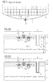
- Figure 1 shows a partial plan view of such a disc-shaped Object, as he, for example, as ultra-thin Semiconductor wafer 1A is known.
- the ultrathin semiconductor wafer 1A which is a Variety of integrated semiconductor circuits or chips 3 with intervening sawing or scratching frame 4, about its peripheral edge 2 on a support point AP, for example laid out in a horde.
- a support point AP Under a sawing or Scribe frame 4 is subsequently the distance between two semiconductor circuits 3 understood, usually for separating or sawing is needed.
- support AP will be As a result, bearing reactions generated, resulting in undesirable Yield shear stresses.
- monocrystalline Semiconductor material such as silicon, which is commonly used for semiconductor wafers, almost no shear stresses endures, now arises according to FIG 1 a hairline crack 5 in the region of the contact point AP.
- such Hairline cracks 5 plant very easily especially in ultrathin semiconductor wafers 1A, which is why they are an essential Cause of the extremely high risk of breakage represent in such ultrathin semiconductor wafers.
- the carrier substrates are semiconductor wafers and In particular, silicon wafers of a first conductivity type are used and formed therein vertical power transistors. In this way, in particular power semiconductor components be made particularly easy and effective.
- electroplating mask is preferably a photosensitive Lacquer with a thickness of 20 .mu.m to 200 .mu.m spin-coated all over and introduced into the trench and then structured by photolithography. Especially when using a negative resist as a photosensitive lacquer is obtained here the desired very steep flanks after structuring of the photoresist.
- galvanic filling material is preferably a variety of galvanically formed metal layers, wherein in particular a Cu / NiP layer sequence for "wire bond" or a Cu / AuSn layer sequence for soldering processes sufficient mechanical stability and high conductivity with good Solderability has.
- shear stress resistant material is high temperature resistant Plastic in between the electroplating filler filled exposed areas, in particular Spun on polyimide or photoimide and etched back or is removed photolithographically by exposure.
- a carrier substrate 1 consists, for example, of a semiconductor wafer and in particular of a monocrystalline silicon semiconductor wafer of a first conductivity type n - with a conventional initial thickness D A of approximately 500 to 1000 ⁇ m.
- semiconductor components such as vertical power transistors with a source region S, a gate G and a drain D may be formed in the carrier substrate 1, wherein in the present embodiment, formed in a trench vertical power transistor in the semiconductor substrate 1 is formed such that its drain region D substantially corresponds to the semiconductor substrate 1, on the surface of a transistor body B is formed as a p-well, in turn, the source regions S and an associated source contact SK for connecting the source regions S are formed on the surface of the transistor B.
- trenches on the surface of the carrier substrate 1, which extend beyond the transistor body B into the semiconductor substrate 1.
- these trenches have, for example, at their trench surface a gate dielectric GD and an electrically conductive gate layer, preferably of highly doped polysilicon as the gate G, whereby a vertical channel region can be realized along the trenches in the transistor body B.
- a device structure further comprises an insulating layer I on the surface of the semiconductor substrate, which is preferably formed thermally as SiO 2 layer.
- a deep trench T with a trench depth h of for example 5 to 200 microns at the front of the carrier substrate or semiconductor wafer 1 is formed.
- the saw frame according to Figure 1 is essentially a grid-shaped Structure has and the individual integrated Circuits and semiconductor devices 3 spaced from each other are, even those trained in the saw frame 4 have Trenches T essentially a grid-shaped structure.
- a trench width is used here depending on a used Filling material dimensioned so that later to be introduced filler as easy as possible in the trenches T can be introduced.
- the trenches have T a trench width of 5 to 100 microns and can therefore be easily housed within the saw frame 4.
- an electric conductive electroplating seed layer or a so-called Electroplating Seed Layer SL on the surface of the carrier substrate and thus also formed on the surface of the trench T.
- This electroplating seed layer SL in this case provides an electrode connection for the later to be carried out electrochemical Electroplating, in particular, to avoid a Indiffusion of impurities from a galvanic deposited metal layer preferably a diffusion barrier layer having.
- PVD process Physical Vapor Deposition
- This is a photoresist with a thickness of 20 microns to Spun 200 .mu.m, and patterned photolithographically.
- a negative resist or negative resist with a thickness of about 150 microns and a subsequent Exposure by means of an "EVG Proximity Printers" receives for the electroplating mask R, the desired ones are especially steep flanks.
- negative varnish for example, the of Sumitomo sold photoresist "Su8" can be used.
- the exposure mask for this electroplating mask R corresponds this usually a mask for a first metallization, why according to the invention no additional exposure masks needed.
- the galvanization mask is in the area of the saw frame according to Figure 2C has exactly one width of the trench T can they also at this point in particular wider than the ditch T be.
- the electroplating mask S at least in the range of the sawing frame 4 already introduced into the trench it already serves as a stabilizing material, which the breaking strength especially of semiconductor wafers already fundamentally improved for handling.
- a galvanizing metal grows as so-called Galvanic filler GF in the exposed areas the galvanization mask R on, preferably to to the level of a level of the electroplating mask R
- Galvanic filler GF is galvanically formed.
- a Cu / NiP layer sequence as electroplating filler material GF has extremely high mechanical properties High conductivity strength for so-called "wire bond" process on while an alternative Cu / AuSn layer sequence has optimal soldering properties.
- Metal compounds or metal combinations with high strength and good solderability such as eutectic materials of gold and tin or of silver and Tin.
- FIG. 2E shows the plating mask R and the underlying one Electroplating seed layer SL for forming shear stress-resistant Areas away.
- the Photoresist or photoresist by means of plasma etching and the following wet-chemical etching removed or stripped. Subsequently become the thus exposed areas of the electroplating seed layer SL etched wet-chemically, including the electroplating filler GF can easily be etched.
- the electroplating filler GF serves as a mask for removal of the photoresist and the underlying electroplating seed layer.
- a shear stress resistant Material TK filled.
- a shear stress resistant Material TK high temperature resistant plastic used and in particular polyimide or photoimide as shear stress resistant Material TK spin coated all over and subsequently etched back or structured by means of exposure.
- this shear stress resistant Material TK which on the one hand the mechanical stability further improved and on the other hand as passivation or insulation between the metallic ones or electrically conductive galvanic fillers acts.
- this shear stress resistant Material TK as a buffer for mechanical stresses, such as in particular because of different coefficients of expansion can occur during a thermal treatment.
- the carrier substrate is thinned from its rear side to a final thickness D E for the realization of a thinned carrier substrate 1A, the final thickness D E of the thinned carrier substrate 1A being smaller than the trench depth h of the trench T.
- this is a mechanical grinding with subsequent wet-chemical etching, wherein the exposed shear stress-resistant material TK can be used as an etch stop and / or alignment mark.
- the wet-chemical back etching serves in particular to eliminate mechanical stresses which are generated during the grinding process in the semiconductor material.
- a back-side metallization RM can be formed on the rear side of the thinned carrier substrate 1A, which in the present case acts as a drain connection for the drain region D of the power semiconductor.
- a fracture-resistant disk-shaped article and in particular a break-resistant semiconductor wafer in which instead of the usual aluminum metallization by means of LIGA technology, a thick (preferably greater than 100 microns) metal plating is formed galvanically.
- the electrical insulation of the metal plating which simultaneously constitute the "bond pads" or connection surfaces for a solder connection, takes place here by means of shear stress-resistant material and in particular by polymer layers of the same thickness. To reduce the mechanical stresses over the entire semiconductor wafer, this shear stress-resistant material is formed in particular in the spaces between the chips or semiconductor devices 3, ie in the saw frame 4.
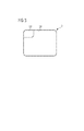
- an extremely simple power semiconductor module is obtained with one in a corner of the building block formed gate connection area or gate pad GP and a in the remaining area formed source connection area or Sourcepad SP. While the source terminal area SP over the 2F shown source contacts FK and the electroplating seed layer SL directly with those formed in the semiconductor substrate 1A Power transistors or their source regions S in Connection is the gate connection area GP via the shear stress resistant material TK electrically isolated from the source connection area SP and only at one not shown Area with the gate strata running in the trenches G electrically connected.
- a drain connection area or drain pad DP is identical to the backside metallization RM and thus with the thinned semiconductor substrate electrically connected, which implements the drain region D.
- the invention has been described above with reference to a silicon semiconductor wafer described. It is not limited to this and similarly includes other carrier substrates. In the same way can as shear stress resistant materials also uses materials other than photimide or polyimide become.
Landscapes
- Electrodes Of Semiconductors (AREA)
- Internal Circuitry In Semiconductor Integrated Circuit Devices (AREA)
- Electroplating Methods And Accessories (AREA)
- Processing Of Stones Or Stones Resemblance Materials (AREA)
Abstract
Description
Claims (23)
- Verfahren zur Herstellung eines bruchfesten scheibenförmigen Gegenstands mit den Schritten:a) Vorbereiten eines Trägersubstrats (1, B, I) mit einer Anfangsdicke (DA) und einem Sägerahmen (4);b) Ausbilden von zumindest einem Graben (T) mit einer Grabentiefe (h) im Wesentlichen im Bereich des Sägerahmens (4) an einer Vorderseite des Trägersubstrats (1, B, I);c) Ausbilden einer elektrisch leitenden Galvanik-Keimschicht (SL) an der Oberfläche des Trägersubstrats und des Grabens (T);d) Ausbilden einer Galvanisierungsmaske (R) mit freiliegenden Galvanik-Bereichen an der Oberfläche der Galvanik-Keimschicht (SL) zumindest im Bereich des Sägerahmens (4);e) Durchführen einer Galvanisierung der Galvanik-Keimschicht (SL) zum Auffüllen der freiliegenden Galvanik-Bereiche mit einem Galvanik-Füllmaterial (GF);f) Entfernen der Galvanisierungsmaske (R) und der darunterliegenden Galvanik-Keimschicht (SL) zum Ausbilden von schubspannungsfesten Bereichen;g) Auffüllen der schubspannungsfesten Bereiche mit einem schubspannungsfesten Material (TK); undh) Dünnen des Trägersubstrats (1) von seiner Rückseite bis zu einer Enddicke (DE) zur Realisierung eines gedünnten Trägersubstrats (1A), wobei die Enddicke (DE) des gedünnten Trägersubstrats (1A) kleiner ist als die Grabentiefe (h) des Grabens (T).
- Verfahren nach Patentanspruch 1,
dadurch gekennzeichnet, dass in Schritt a) in einem Halbleiterwafer (1) von einem ersten Leitungstyp (n-) vertikale Leistungstransistoren (S, G, D) ausgebildet werden. - Verfahren nach Patentanspruch 1 oder 2,
dadurch gekennzeichnet, dass in Schritt b) ein Laserschneiden, Plasmaätzen, nasschemisches Ätzen, lichtinduziertes Ätzen, anodisches Ätzen und/oder Sägen durchgeführt wird. - Verfahren nach einem der Patentansprüche 1 bis 3,
dadurch gekennzeichnet, dass in Schritt c) ein PVD-Verfahren zum ganzflächigen Ausbilden der Galvanik-Keimschicht (SL) durchgeführt wird. - Verfahren nach Patentanspruch 4,
dadurch gekennzeichnet, dass die Galvanik-Keimschicht (SL) eine Diffusionsbarierenschicht aufweist. - Verfahren nach Patentanspruch 4 oder 5,
dadurch gekennzeichnet, dass die Galvanik-Keimschicht (SL) eine TaN/Cu- oder TiN/Cu-Schichtenfolge mit einer Dicke kleiner 100nm aufweist. - Verfahren nach einem der Patentansprüche 1 bis 6,
dadurch gekennzeichnet, dass in Schritt d) ein fotosensitiver Lack mit einer Dicke von 20µm bis 200µm ganzflächig aufgeschleudert sowie in den zumindest einen Graben (T) eingebracht und zur Ausbildung der Galvanisierungsmaske (R) fotolithographisch strukturiert wird. - Verfahren nach Patentanspruch 7,
dadurch gekennzeichnet, dass der fotosensitive Lack einen Negativresist darstellt. - Verfahren nach einem der Patentansprüche 1 bis 8,
dadurch gekennzeichnet, dass in Schritt e) eine Vielzahl von galvanischen Metallschichten und insbesondere eine Cu/NiP- oder Cu/AuSn-Schichtenfolge als Galvanik-Füllmaterial (GF) ausgebildet wird. - Verfahren nach einem der Patentansprüche 1 bis 9,
dadurch gekennzeichnet, dass in Schritt f) ein Plasma-Ätzen mit nasschemischen Ätzen zum Entfernen der Galvanisierungsmaske (R) und
ein weiteres nasschemisches Ätzen zum Entfernen der darunterliegenden Galvanik-Keimschicht (SL) unter Verwendung des Galvanik-Füllmaterials (GF) als Maske durchgeführt wird. - Verfahren nach einem der Patentansprüche 1 bis 10,
dadurch gekennzeichnet, dass in Schritt g) als schubspannungsfestes Material (TK) hochtemperaturfester Kunsstoff aufgefüllt wird. - Verfahren nach Patentanspruch 11,
dadurch gekennzeichnet, dass als schubspannungsfestes Material (TK) Polyimid oder Fotoimid aufgeschleudert und rückgeätzt wird. - Verfahren nach einem der Patentansprüche 1 bis 12,
dadurch gekennzeichnet, dass in Schritt h) ein mechanisches Schleifen mit nachfolgendem nasschemischen Ätzen durchgeführt wird. - Verfahren nach einem der Patentansprüche 1 bis 13,
dadurch gekennzeichnet, dass in Schritt h) bis zu einer Enddicke (DE) von 5 µm bis 200 µm gedünnt wird. - Verfahren nach einem der Patentansprüche 1 bis 14,
gekennzeichnet durch
den weiteren Schritt i) Ausbilden einer Rückseitenmetallisierung (RM) an der Rückseite des gedünnten Trägersubstrats (1A). - Halbleiterschaltungsanordnung mit
einem gedünnten Trägersubstrat (1A, B, I), in dem zumindest ein Halbleiterbauelement (S, G, D) ausgebildet ist;
einer Galvanik-Keimschicht (SL), die zumindest teilweise an der Oberfläches des gedünnten Trägersubstrats (1A, B, I) ausgebildet ist;
einem Galvanik-Füllmaterial (GF), das an der Oberfläche der Galvanik-Keimschicht (SL) galvanisch ausgebildet ist; und einem schubspannungsfesten Material (TK), das an der nicht von der Galvanik-Keimschicht (SL) bedeckten Oberfläche des gedünnten Trägersubstrats (1A, B, I) im Wesentlichen bis zu einer Höhe des Galvanik-Füllmaterials (GF) ausgebildet ist. - Halbleiterschaltungsanordnung nach Patentanspruch 16, dadurch gekennzeichnet, dass das gedünnte Trägersubstrat einen gedünnten Halbleiterwafer (1A) von einem ersten Leitungstyp (n-) und
das zumindest eine Halbleiterbauelement einen vertikalen Leistungstransistore (S, G, D) aufweist. - Halbleiterschaltungsanordnung nach Patentanspruch 16 oder 17, dadurch gekennzeichnet, dass die Galvanik-Keimschicht (SL) eine Diffusionsbarierenschicht aufweist.
- Halbleiterschaltungsanordnung nach einem der Patentansprüche 16 bis 18, dadurch gekennzeichnet, dass die Galvanik-Keimschicht (SL) eine TaN/Cu- oder TiN/Cu-Schichtenfolge mit einer Dicke kleiner 100nm aufweist.
- Halbleiterschaltungsanordnung nach einem der Patentansprüche 16 bis 19, dadurch gekennzeichnet, dass das Galvanik-Füllmaterial (GF) eine Vielzahl von galvanischen Metallschichten und insbesondere eine Cu/NiPoder Cu/AuSn-Schichtenfolge aufweist.
- Halbleiterschaltungsanordnung nach einem der Patentansprüche 16 bis 20, dadurch gekennzeichnet, dass das schubspannungsfeste Material (TK) einen hochtemperaturfesten Kunsstoff und insbesondere Polyimid oder Fotoimid aufweist.
- Halbleiterschaltungsanordnung nach einem der Patentansprüche 16 bis 21, dadurch gekennzeichnet, dass eine Dicke des gedünnten Trägersubstrats (1A, B, I) in einem Bereich von 5 µm bis 200 µm und eine Dicke der Galvanik-Füllmaterials (GF) und des schubspannungsfesten Materials (TK) in einem Bereich von 200 µm bis 20 µm liegt.
- Halbleiterschaltungsanordnung nach einem der Patentansprüche 16 bis 22, dadurch gekennzeichnet, dass an der Rückseite des gedünnten Trägersubstrats (1A) eine Rückseitenmetallisierung (RM) ausgebildet ist.
Applications Claiming Priority (2)
| Application Number | Priority Date | Filing Date | Title |
|---|---|---|---|
| DE10326508 | 2003-06-12 | ||
| DE10326508A DE10326508A1 (de) | 2003-06-12 | 2003-06-12 | Verfahren zur Herstellung eines bruchfesten scheibenförmigen Gegenstands sowie zugehörige Halbleiterschaltungsanordnung |
Publications (3)
| Publication Number | Publication Date |
|---|---|
| EP1505638A2 true EP1505638A2 (de) | 2005-02-09 |
| EP1505638A3 EP1505638A3 (de) | 2009-03-11 |
| EP1505638B1 EP1505638B1 (de) | 2012-02-29 |
Family
ID=33520553
Family Applications (1)
| Application Number | Title | Priority Date | Filing Date |
|---|---|---|---|
| EP04101940A Expired - Lifetime EP1505638B1 (de) | 2003-06-12 | 2004-05-05 | Verfahren zur Herstellung eines bruchfesten, scheibenförmigen Gegenstands sowie zugehörige Halbleiterschaltungsanordnung |
Country Status (2)
| Country | Link |
|---|---|
| EP (1) | EP1505638B1 (de) |
| DE (1) | DE10326508A1 (de) |
Cited By (1)
| Publication number | Priority date | Publication date | Assignee | Title |
|---|---|---|---|---|
| US12559853B2 (en) | 2019-07-26 | 2026-02-24 | Lam Research Corporation | Differential contrast plating for advanced packaging applications |
Citations (2)
| Publication number | Priority date | Publication date | Assignee | Title |
|---|---|---|---|---|
| US5691248A (en) | 1995-07-26 | 1997-11-25 | International Business Machines Corporation | Methods for precise definition of integrated circuit chip edges |
| US20030102563A1 (en) | 2001-11-30 | 2003-06-05 | Mercado Lei L. | Semiconductor power device and method of formation |
Family Cites Families (7)
| Publication number | Priority date | Publication date | Assignee | Title |
|---|---|---|---|---|
| US5104820A (en) * | 1989-07-07 | 1992-04-14 | Irvine Sensors Corporation | Method of fabricating electronic circuitry unit containing stacked IC layers having lead rerouting |
| CA2118994A1 (en) * | 1993-06-21 | 1994-12-22 | Claude L. Bertin | Polyimide-insulated cube package of stacked semiconductor device chips |
| US5618752A (en) * | 1995-06-05 | 1997-04-08 | Harris Corporation | Method of fabrication of surface mountable integrated circuits |
| EP2270846A3 (de) * | 1996-10-29 | 2011-12-21 | ALLVIA, Inc. | Integrierte Schaltungen und Verfahren zu ihrer Herstellung |
| US6882030B2 (en) * | 1996-10-29 | 2005-04-19 | Tru-Si Technologies, Inc. | Integrated circuit structures with a conductor formed in a through hole in a semiconductor substrate and protruding from a surface of the substrate |
| US6093966A (en) * | 1998-03-20 | 2000-07-25 | Motorola, Inc. | Semiconductor device with a copper barrier layer and formation thereof |
| DE10326507A1 (de) * | 2003-06-12 | 2005-01-13 | Infineon Technologies Ag | Verfahren zur Herstellung eines bruchfesten scheibenförmigen Gegenstands sowie zugehörige Halbleiterschaltungsanordung |
-
2003
- 2003-06-12 DE DE10326508A patent/DE10326508A1/de not_active Ceased
-
2004
- 2004-05-05 EP EP04101940A patent/EP1505638B1/de not_active Expired - Lifetime
Patent Citations (2)
| Publication number | Priority date | Publication date | Assignee | Title |
|---|---|---|---|---|
| US5691248A (en) | 1995-07-26 | 1997-11-25 | International Business Machines Corporation | Methods for precise definition of integrated circuit chip edges |
| US20030102563A1 (en) | 2001-11-30 | 2003-06-05 | Mercado Lei L. | Semiconductor power device and method of formation |
Cited By (1)
| Publication number | Priority date | Publication date | Assignee | Title |
|---|---|---|---|---|
| US12559853B2 (en) | 2019-07-26 | 2026-02-24 | Lam Research Corporation | Differential contrast plating for advanced packaging applications |
Also Published As
| Publication number | Publication date |
|---|---|
| EP1505638A3 (de) | 2009-03-11 |
| EP1505638B1 (de) | 2012-02-29 |
| DE10326508A1 (de) | 2005-01-13 |
Similar Documents
| Publication | Publication Date | Title |
|---|---|---|
| DE102008016427B4 (de) | Drahtbonden auf reaktiven Metalloberflächen einer Metallisierung eines Halbleiterbauelements durch Vorsehen einer Schutzschicht | |
| DE102012104270B4 (de) | Halbleiterkomponente, Halbleiterkomponentenanordnung und Verfahren zum Herstellen einer Halbleiterkomponente | |
| DE102013112797B4 (de) | Anordnung mit halbleitervorrichtung einschliesslich eines chipträgers, halbleiterwafer und verfahren zum herstellen einer halbleitervorrichtung | |
| DE102010037941B4 (de) | Verfahren und Verwendung eines rekonstituierten Wafer zur Halbleiterbauelementfabrikation | |
| DE102019127076B4 (de) | Filmstruktur für bondkontaktstelle und verfahren zu ihrer herstellung | |
| DE102008052470B4 (de) | Verfahren zum Prozessieren eines Kontaktpads und Verfahren zum Herstellen eines integrierten Schaltkreiselementes | |
| DE102013111452B4 (de) | Halbleitervorrichtungen und Halbleiterverarbeitungsverfahren | |
| DE10224775A1 (de) | Halbleitervorrichtung | |
| DE102014107557B4 (de) | Verfahren zum Bearbeiten eines Halbleiterwerkstücks | |
| DE102004052921A1 (de) | Verfahren zur Herstellung von Halbleiterbauelementen mit externen Kontaktierungen | |
| DE102009035437A1 (de) | Halbleiterbauelement mit einem Verspannungspuffermaterial, das über einem Metallisierungssystem mit kleinem ε gebildet ist | |
| DE102015102579B4 (de) | Halbleitervorrichtungen und Verfahren zur Ausbildung davon | |
| DE102011050953B4 (de) | Halbleitervorrichtung und Verfahren zu deren Herstellung | |
| DE102012111520B4 (de) | Leiterrahmen-freies und Die-Befestigungsprozess-Material-freies Chipgehäuse und Verfahren zum Bilden eines Leiterrahmen-freien und Die-Befestigungsprozess-Material-freien Chipgehäuses | |
| DE102017109670B4 (de) | Herstellungsverfahren für ein Chippackage mit Seitenwandmetallisierung | |
| DE102013106378B4 (de) | Verfahren zur herstellung eines chipgehäuses | |
| DE102006030266A1 (de) | Verringern der Kontamination von Halbleitersubstraten während der Metallisierungsbearbeitung durch Bereitstellen einer Schutzschicht am Substratrand | |
| DE102013110541A1 (de) | Integrierte schaltung, chipgehäuse und verfahren zur herstellung einer integrierten schaltung | |
| DE102016114814B4 (de) | Halbleitervorrichtung und Herstellungsverfahren | |
| DE20208866U1 (de) | Kontaktierte und gehäuste integrierte Schaltung | |
| DE102008036285B4 (de) | Integrierte Schaltung mit einer durch einen galvanischen Prozess erzeugten Verbindung mit einem Kühlkörper und Verfahren dazu | |
| DE102009030957B4 (de) | Verfahren zum Herstellen einer Halbleiteranordnung mittels Ätzung eines Halbleiterchips und Halbleiteranordnung | |
| DE102006056620B4 (de) | Halbleiterstruktur und Verfahren zu ihrer Herstellung | |
| EP1505638B1 (de) | Verfahren zur Herstellung eines bruchfesten, scheibenförmigen Gegenstands sowie zugehörige Halbleiterschaltungsanordnung | |
| DE102016122637A1 (de) | Verfahren zur Verwendung beim Herstellen von Halbleitervorrichtungen |
Legal Events
| Date | Code | Title | Description |
|---|---|---|---|
| PUAI | Public reference made under article 153(3) epc to a published international application that has entered the european phase |
Free format text: ORIGINAL CODE: 0009012 |
|
| AK | Designated contracting states |
Kind code of ref document: A2 Designated state(s): AT BE BG CH CY CZ DE DK EE ES FI FR GB GR HU IE IT LI LU MC NL PL PT RO SE SI SK TR |
|
| AX | Request for extension of the european patent |
Extension state: AL HR LT LV MK |
|
| PUAL | Search report despatched |
Free format text: ORIGINAL CODE: 0009013 |
|
| AK | Designated contracting states |
Kind code of ref document: A3 Designated state(s): AT BE BG CH CY CZ DE DK EE ES FI FR GB GR HU IE IT LI LU MC NL PL PT RO SE SI SK TR |
|
| AX | Request for extension of the european patent |
Extension state: AL HR LT LV MK |
|
| 17P | Request for examination filed |
Effective date: 20090326 |
|
| 17Q | First examination report despatched |
Effective date: 20090507 |
|
| AKX | Designation fees paid |
Designated state(s): DE FR GB |
|
| RAP1 | Party data changed (applicant data changed or rights of an application transferred) |
Owner name: INFINEON TECHNOLOGIES AG |
|
| RIC1 | Information provided on ipc code assigned before grant |
Ipc: H01L 21/288 20060101AFI20110314BHEP |
|
| APBK | Appeal reference recorded |
Free format text: ORIGINAL CODE: EPIDOSNREFNE |
|
| APBN | Date of receipt of notice of appeal recorded |
Free format text: ORIGINAL CODE: EPIDOSNNOA2E |
|
| APBR | Date of receipt of statement of grounds of appeal recorded |
Free format text: ORIGINAL CODE: EPIDOSNNOA3E |
|
| REG | Reference to a national code |
Ref country code: DE Ref legal event code: R079 Ref document number: 502004013333 Country of ref document: DE Free format text: PREVIOUS MAIN CLASS: H01L0021300000 Ipc: H01L0023544000 |
|
| APBV | Interlocutory revision of appeal recorded |
Free format text: ORIGINAL CODE: EPIDOSNIRAPE |
|
| RIC1 | Information provided on ipc code assigned before grant |
Ipc: H01L 23/544 20060101AFI20110912BHEP Ipc: H01L 21/288 20060101ALI20110912BHEP |
|
| GRAC | Information related to communication of intention to grant a patent modified |
Free format text: ORIGINAL CODE: EPIDOSCIGR1 |
|
| GRAP | Despatch of communication of intention to grant a patent |
Free format text: ORIGINAL CODE: EPIDOSNIGR1 |
|
| GRAS | Grant fee paid |
Free format text: ORIGINAL CODE: EPIDOSNIGR3 |
|
| GRAA | (expected) grant |
Free format text: ORIGINAL CODE: 0009210 |
|
| RIN1 | Information on inventor provided before grant (corrected) |
Inventor name: GRASSMANN, ANDREAS |
|
| AK | Designated contracting states |
Kind code of ref document: B1 Designated state(s): DE FR GB |
|
| REG | Reference to a national code |
Ref country code: GB Ref legal event code: FG4D Free format text: NOT ENGLISH |
|
| REG | Reference to a national code |
Ref country code: DE Ref legal event code: R096 Ref document number: 502004013333 Country of ref document: DE Effective date: 20120426 |
|
| PLBE | No opposition filed within time limit |
Free format text: ORIGINAL CODE: 0009261 |
|
| STAA | Information on the status of an ep patent application or granted ep patent |
Free format text: STATUS: NO OPPOSITION FILED WITHIN TIME LIMIT |
|
| 26N | No opposition filed |
Effective date: 20121130 |
|
| REG | Reference to a national code |
Ref country code: DE Ref legal event code: R097 Ref document number: 502004013333 Country of ref document: DE Effective date: 20121130 |
|
| REG | Reference to a national code |
Ref country code: FR Ref legal event code: PLFP Year of fee payment: 13 |
|
| REG | Reference to a national code |
Ref country code: FR Ref legal event code: PLFP Year of fee payment: 14 |
|
| PGFP | Annual fee paid to national office [announced via postgrant information from national office to epo] |
Ref country code: FR Payment date: 20170523 Year of fee payment: 14 Ref country code: GB Payment date: 20170519 Year of fee payment: 14 |
|
| PGFP | Annual fee paid to national office [announced via postgrant information from national office to epo] |
Ref country code: DE Payment date: 20170718 Year of fee payment: 14 |
|
| REG | Reference to a national code |
Ref country code: DE Ref legal event code: R119 Ref document number: 502004013333 Country of ref document: DE |
|
| GBPC | Gb: european patent ceased through non-payment of renewal fee |
Effective date: 20180505 |
|
| PG25 | Lapsed in a contracting state [announced via postgrant information from national office to epo] |
Ref country code: DE Free format text: LAPSE BECAUSE OF NON-PAYMENT OF DUE FEES Effective date: 20181201 Ref country code: GB Free format text: LAPSE BECAUSE OF NON-PAYMENT OF DUE FEES Effective date: 20180505 Ref country code: FR Free format text: LAPSE BECAUSE OF NON-PAYMENT OF DUE FEES Effective date: 20180531 |