EP1497973B1 - Abbildungseinrichtung und zeitsteuerungsgenerator - Google Patents
Abbildungseinrichtung und zeitsteuerungsgenerator Download PDFInfo
- Publication number
- EP1497973B1 EP1497973B1 EP03713171A EP03713171A EP1497973B1 EP 1497973 B1 EP1497973 B1 EP 1497973B1 EP 03713171 A EP03713171 A EP 03713171A EP 03713171 A EP03713171 A EP 03713171A EP 1497973 B1 EP1497973 B1 EP 1497973B1
- Authority
- EP
- European Patent Office
- Prior art keywords
- timing
- timing generator
- signal
- output
- controller
- Prior art date
- Legal status (The legal status is an assumption and is not a legal conclusion. Google has not performed a legal analysis and makes no representation as to the accuracy of the status listed.)
- Expired - Lifetime
Links
- 238000003384 imaging method Methods 0.000 title claims abstract description 39
- 238000012545 processing Methods 0.000 claims abstract description 13
- 230000001360 synchronised effect Effects 0.000 claims description 4
- 230000004044 response Effects 0.000 claims description 3
- 230000006870 function Effects 0.000 description 11
- 238000000034 method Methods 0.000 description 7
- 238000003860 storage Methods 0.000 description 6
- 230000008859 change Effects 0.000 description 5
- 230000008569 process Effects 0.000 description 5
- 238000013461 design Methods 0.000 description 4
- 238000010586 diagram Methods 0.000 description 4
- 238000000605 extraction Methods 0.000 description 3
- 230000006399 behavior Effects 0.000 description 2
- 230000008901 benefit Effects 0.000 description 2
- 230000003247 decreasing effect Effects 0.000 description 2
- 230000000977 initiatory effect Effects 0.000 description 2
- 230000001343 mnemonic effect Effects 0.000 description 2
- 238000012546 transfer Methods 0.000 description 2
- 238000013459 approach Methods 0.000 description 1
- 230000001143 conditioned effect Effects 0.000 description 1
- 239000013078 crystal Substances 0.000 description 1
- 230000001419 dependent effect Effects 0.000 description 1
- 238000009826 distribution Methods 0.000 description 1
- 230000000694 effects Effects 0.000 description 1
- 238000004519 manufacturing process Methods 0.000 description 1
- 238000012986 modification Methods 0.000 description 1
- 230000004048 modification Effects 0.000 description 1
- 230000003252 repetitive effect Effects 0.000 description 1
- 230000011664 signaling Effects 0.000 description 1
- 230000009131 signaling function Effects 0.000 description 1
- 230000003068 static effect Effects 0.000 description 1
Images


Classifications
-
- H—ELECTRICITY
- H04—ELECTRIC COMMUNICATION TECHNIQUE
- H04N—PICTORIAL COMMUNICATION, e.g. TELEVISION
- H04N23/00—Cameras or camera modules comprising electronic image sensors; Control thereof
- H04N23/60—Control of cameras or camera modules
- H04N23/617—Upgrading or updating of programs or applications for camera control
-
- G—PHYSICS
- G09—EDUCATION; CRYPTOGRAPHY; DISPLAY; ADVERTISING; SEALS
- G09G—ARRANGEMENTS OR CIRCUITS FOR CONTROL OF INDICATING DEVICES USING STATIC MEANS TO PRESENT VARIABLE INFORMATION
- G09G5/00—Control arrangements or circuits for visual indicators common to cathode-ray tube indicators and other visual indicators
- G09G5/18—Timing circuits for raster scan displays
-
- H—ELECTRICITY
- H04—ELECTRIC COMMUNICATION TECHNIQUE
- H04N—PICTORIAL COMMUNICATION, e.g. TELEVISION
- H04N23/00—Cameras or camera modules comprising electronic image sensors; Control thereof
- H04N23/60—Control of cameras or camera modules
- H04N23/665—Control of cameras or camera modules involving internal camera communication with the image sensor, e.g. synchronising or multiplexing SSIS control signals
-
- H—ELECTRICITY
- H04—ELECTRIC COMMUNICATION TECHNIQUE
- H04N—PICTORIAL COMMUNICATION, e.g. TELEVISION
- H04N25/00—Circuitry of solid-state image sensors [SSIS]; Control thereof
-
- H—ELECTRICITY
- H04—ELECTRIC COMMUNICATION TECHNIQUE
- H04N—PICTORIAL COMMUNICATION, e.g. TELEVISION
- H04N25/00—Circuitry of solid-state image sensors [SSIS]; Control thereof
- H04N25/70—SSIS architectures; Circuits associated therewith
- H04N25/71—Charge-coupled device [CCD] sensors; Charge-transfer registers specially adapted for CCD sensors
- H04N25/745—Circuitry for generating timing or clock signals
-
- H—ELECTRICITY
- H04—ELECTRIC COMMUNICATION TECHNIQUE
- H04N—PICTORIAL COMMUNICATION, e.g. TELEVISION
- H04N25/00—Circuitry of solid-state image sensors [SSIS]; Control thereof
- H04N25/70—SSIS architectures; Circuits associated therewith
- H04N25/76—Addressed sensors, e.g. MOS or CMOS sensors
- H04N25/7795—Circuitry for generating timing or clock signals
-
- H—ELECTRICITY
- H04—ELECTRIC COMMUNICATION TECHNIQUE
- H04N—PICTORIAL COMMUNICATION, e.g. TELEVISION
- H04N5/00—Details of television systems
- H04N5/04—Synchronising
- H04N5/06—Generation of synchronising signals
Definitions
- the invention relates to imaging devices and timing generators for generating timing signals in an imaging device.
- the timing signals are generated by means of a timing generator.
- the timing generators are implemented as complex state machines that are designed to provide timing signals to a specific imaging system implemented by means of a specific set of components.
- a new timing generator has to be manufactured for every new imaging system and every time a component in an existing imaging system is exchanged for another one of said component.
- To design and produce a new timing generator every time a signal has to be added or altered is time-consuming and expensive.
- the timing generator includes a line control unit for generating a lower level waveform, a frame control unit and an arbitrator.
- the arbitrator control the distribution of waveform control words to the line control unit and the frame control unit.
- the control of the arbitrator is based on signals provided from the line control unit and the frame control unit, respectively. Said signals being a signal from the frame control unit regarding an ended frame cycle and signals from the line control unit regarding an ended cycle or a reception of the next line type.
- the system generates a signal in accordance with a waveform control word including the level of each timing signal and a value indicating the number of cycles this word defines the levels of the timing signals.
- a waveform control word including the level of each timing signal and a value indicating the number of cycles this word defines the levels of the timing signals.
- timing generator above is more flexible than a prior art state machine. However, in some situations said timing generator may require a lot of memory and much effort may be required for setting the waveform control words.
- the timing generator disclosed comprises a ROM for storing time sequential data for the repetitive pattern of the logical level of an output pulse, V and H counters counting vertical and horizontal synchronisation pulses, ROMs for storing edge data determining at which H and V values the level of a control pulse is to be changed. Then the timing signals are generated from the output pulse and the control pulse by combining them in a logic circuit.
- the structure and functionality of the timing generator results in that the data to be stored in ROM has to be specified for all signals sent to the MIX and for every instance in time. Further, these signals, sent to the MIX from the ROM, and the logical functionality of the MIX has to be considered when providing the ROMs with data. This is also the case in the implementations including an external ROM and/or an external PC for providing data to the system.
- a video timing signal generating circuit based on a small programmable CPU is disclosed.
- the circuit is used to generate timing signals, in particular timing signals used in conjunction with a video monitor.
- a load instruction is arranged to load a pixel backing register and the machine is paused until a counter, which has been loaded with a timer value by the program, then the contents of the backing register are copied into an output signal register which drives the CSYNC, VSYNC, HSYNC signals, the blanking signal and the pixel clock enable signal.
- the programmer of the timing signal generating circuit has to keep track the timing of the circuit by means of keeping track of timer values and program lines in order to keep the correct timing of the circuit. Additionally, the programmer has to know the required signal level of every output signal at every instance in time and enter those levels into an instruction SRAM.
- a timing generator for an imaging system comprises: an output timing signal controller, which output timing signal controller is arranged to provide a plurality of output signals at a plurality of signal lines thereof, an horizontal position counter and a vertical position counter arranged to count clock cycles for keeping track of an x and y coordinate of a pixel presently handled.
- said timing generator includes a programmable program memory that is arranged to comprise program instructions for controlling the generation of timing signals and a timing generator controller for processing the program instructions from the program memory.
- the timing generator controller includes a decoder for decoding program instructions from the memory, the decoder being arranged to output at least one control signal and a plurality of parallel signals forming a bit pattern and constituting an output timing signal specification, the output timing signal specification determining the appearance of the output signals in response to the decoding of said instructions.
- the output timing signal controller is connected to the timing generator controller for reception of the at least one control signal and the output timing signal specification.
- the output timing signal controller further comprises means for performing an XOR operation and comprising at least one selector, said means for performing an XOR operation being arranged to receive said plurality of output signals, to receive said output timing signal specification or a bit pattern of zeros from the selector depending on the at least one control signal, and to output signals resulting from the XOR operation between the signals from the selector and said plurality of output signals.
- the output from the means for performing an XOR operation is connected to the plurality of signal lines of the output timing signal controller.
- a timing generator controller including a decoder of program instructions and an output signal controller responsive to at least one control signal and a timing signal specification, which are provided by the timing generator controller
- the decoder is able to interpret program instructions and provide control signals at least to devices in the timing generator that are to be affected by a presently executed program instruction.
- the program instructions can be defined as sophisticated control instructions, which in most cases make the programming easy.
- the instruction codes may be assigned to mnemonics and a software tool can be arranged to convert a text file comprising a program written using said mnemonics into binary program instruction words that may be stored in a data file. Thereby, the programming may be performed in a language similar to the assembly language of a microprocessor. The data file may then be downloaded to the imaging system and be used in the timing generator.
- the timing generator controller includes a stack for storing at least one return address to at least one program instruction in the program memory, the program instruction being the program instruction that is to be executed when the end of a subroutine has been reached.
- the program in the program memory only has to include one copy of a procedure or function that is frequently used.
- Program instructions for subroutine jumps can be inserted anywhere in the execution sequence of a program and as many times as needed. This results in that memory can be saved, because a frequently utilised procedure or function only has to be stored once in the program memory, and that the programming of the timing generator becomes easier, especially for complex timing signal sets, because a person programming only has to write the program instructions of the subroutine once instead of repeating corresponding functionality in every location in the program where it should be executed.
- the timing generator controller includes a register bank, wherein the register bank includes a register that the timing generator is able to read and at least one system external to the timing generator is able to write.
- the register By implementing the above register it becomes possible to dynamically change the behaviour of timing signals sent from the timing generator in a process in progress without interrupting said process. This is a result of the register being possible to write from systems external to the timing generator and the register being readable from within the timing generator.
- the instruction dynamically changes whenever the value of the register is changed. This feature may, for example, be advantageous for systems delivering frequently updated images in which some parameter has to be changed during acquisition of an image sequence. Some examples of such parameter is the exposure time, the number of images that are to be sent per second, number of rows in an image, etc.
- the timing generator controller further includes a register bank, wherein the register bank includes a register that is accessible as read and write from the timing generator.
- the timing generator comprises an input signal line for reception of a clock signal for timing the operation of the timing generator, wherein said clock signal is synchronous with a pixel timing signal.
- the timing generator becomes easy to program. This is the case because the pixel timing signal, comprising pixel clock signal cycles, is the most basic timing signal in the imaging system and a signal that most processes depends on.
- a programmer of the timing generator in accordance with this embodiment is able to program the timing generator by considering the number of multiples of pixel clock signal cycles, i.e. cycles of the timing signal that is timing the timing generator.
- the programmable program memory is made accessible by the timing generator controller as read only and is made of a size lesser than or equal to 1 kbyte.
- the restriction of the program memory being accessible as read only by the timing generator controller may result in that there is no need for any devices keeping track of data written to the memory, and in that the size of the memory only has to be of such size that there is room for programs.
- the memory is the portion of the timing generator that requires most space and, thus, by limiting the size of the memory to 1 kbyte the timing generator becomes small. Despite the small size of the memory it is possible to implement complex timing signals because of the features presented above.
- an imaging device comprising an image sensor, an analogue image processor, an analogue to digital (A/D) converter, and a timing generator providing timing signals to the image sensor, the analogue image processor and the A/D converter, wherein the timing generator corresponds to any one of the embodiments mentioned above.
- At least the programmable program memory, the decoder, the output signal line controller and the stack of the timing generator is arranged in one single integrated circuit. This results in that the imaging device and, especially, the timing generator may become inexpensive. Further, such image system may be easy to manufacture because of the fact that it is easier to mount few circuits than a plurality.
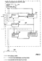
- FIG. 1 an imaging system is partly shown.
- imaging system is typically implemented in a video camera, a surveillance camera, a still camera, a network camera, a web camera, etc.
- the imaging system preferably comprises an image sensor 2, an analogue image processor 4, an analogue to digital converter (A/D-converter) 6, a digital signal processor (DSP) 8, a microprocessor 10, and a timing generator system 12.
- A/D-converter an analogue to digital converter
- DSP digital signal processor
- the image system captures an image via reflected light defining the image.
- the reflected light is preferably captured by a lens system, not shown, and directed onto the image sensor 2, which could be a Charge Coupled Device (CCD) or a CMOS-type image sensor.
- the image sensor 2 is controlled by means of a plurality of timing signals 14 that is provided by the timing generator system 12. The required signal function over time for such timing signals 14 may vary a lot for different image sensors, even the operations controlled by the timing signals 14 may vary for different image sensors.
- the image captured by the image sensor 2 is represented by analogue, electrical signals and is passed to the analogue image processor 4 when the image sensor 2 has been exposed to the light during a specific time period.
- the function of such analogue image processors 4 is known by the person skilled in the art.
- the analogue image processor 4 also need timing signals 16 for proper operation. These timing signals 16 are also provided by the timing generator system 12.
- the timing signals 16 controlling the analogue image processor 4 may also have to be varied depending on the analogue image processor 4 used in the system.
- the analogue image processor 4 When the analogue image processor 4 has processed the analogue representation of the image, the image is converted to digital information by means of the A/D-converter 6. In most imaging systems the A/D-converter 6 also need to be timed by means of at least one timing signal 18. In one embodiment of the invention such timing is performed by means of the timing generator system 12.
- DSP digital signal processor
- the processed digital image is then passed to a system 22 for processing the digital image in accordance with the overall purpose of the imaging system.
- said processing could include coding of the image in accordance with a coding standard, e.g. JPEG, MPEG, PAL, generating an image and/or video file for storage in an external or internal memory, or arranging the image data for transfer via a network, e.g. a telephone network, a computer network, a network for television signals, a surveillance network.
- a network e.g. a telephone network, a computer network, a network for television signals, a surveillance network.
- the imaging system comprises a microprocessor 10 arranged for controlling the overall performance of the imaging system.
- the microprocessor is also enabled to provide parameters to the timing generator system 12 in order to affect the capturing of images.
- the timing generator system 12 is arranged to generate the timing signals that are required by the imaging system.
- the timing generator system 12, according to one embodiment, is a programmable timing generator system 12 in which the function over time of the timing signals are easy to program, and alter. According to a specific embodiment the timing signals are easy to change dynamically during the capture of an image sequence.
- the timing generator system comprises horizontal and vertical position counters (H/V counters) 204, for keeping track of the coordinates of the pixel in the image sensor that is presently handled, a pixel clock generator 206, for providing high frequency timing signals, a programmable program memory 220, a timing generator controller 222, and an output timing signal controller 236.
- the timing generator system may be implemented in one Integrated Circuit (IC). However, some parts of the timing generator system may be implemented separate from such IC.
- the pixel clock generator 206 receives a high frequency clock signal from a crystal and generates, from this high frequency clock signal, high frequency timing signals of the imaging system, e.g. it provides the timing generator 202 with a timing signal 208 of pixel clock frequency used for timing of the processing in the timing generator 202 and it provides the image sensor of the imaging system with timing signals of pixel clock frequency.
- the pixel clock generator 206 may provide timing signals having a pixel clock cycle to other devices than the timing generator 202 and the image sensor.
- the pixel clock generator 206 may provide an output signal of pixel clock frequency to the image sensor as horizontal CCD drive or corresponding signal, to the timing generator 202, a sample and hold pulse to the analogue image processor, a clock signal to the A/D converter, etc.
- the pixel clock generator 206 generates the most basic timing signals, which other more advanced timing signals may be based on. By basing the processing cycles of the timing generator on the pixel clock signal cycle it is easy to program the output timing signals as functions of either the pixel clock signal cycle or the execution cycle of the program.
- the pixel clock generator 206 may receive a timing signal from the output signal controller 236. Such signal is arranged for controlling the output of some of the timing signals from the pixel clock generator 206.
- the control signal may act as a gate signal, thus stopping the controlled signals from reaching their destination or letting the controlled signals pass through to their destinations.
- the H/V counters 204 is a set of counters arranged to count clock cycles in order to keep track of the x and y coordinate of the pixel presently handled and to provide this information to the timing generator 202. In order to manage this the H/V counters 204 receive at least one timing signal from the pixel clock, the timing signal corresponds to the signal timing the processing of each pixel, i.e. pixel clock. Further, the H/V counters 204 utilises registers in which the microprocessor stores a value indicating the number of pixels that are to be interpreted as one row of an image and a value indicating the number of rows that are to be interpreted as one image frame.
- an x-coordinate counter counts every timing cycle from the pixel clock generator 206 and is reset when it has counted a number of pixels corresponding to the stored value that indicates the number of pixels in a row.
- This reset signal also trigger an y-coordinate counter, which is reset when it has counted a number of rows corresponding to the stored value that indicates the number of rows in an image frame.
- the counter may also be implemented to count the y-coordinates in the way the x-coordinates is counted above and to count the x-coordinates in the in the way the y-coordinates is counted above. In such case the value that indicates the number of pixels in a row instead indicates the number of pixels in a column.
- the H/V counters 204 counts all clock cycles, even those occurring during blanking periods, i.e. the period when no pixel data is outputted from the image sensor.
- the programmable program memory 220 is arranged to store the program instructions controlling the timing generator and its output signals.
- the programmable program memory 220 is enabled to be programmed from an external source, for example an external computer connecting with the imaging device or the microprocessor within the imaging device.
- the microprocessor provide a program to the programming memory during initiation of the imaging system.
- the program may also be provided from the microprocessor in connection with a user selection of image format or similar. In such case it may be possible to store different programs for different imaging functionalities or imaging formats in a memory of the microprocessor, the program being downloaded to the program memory 220 when a change in function or format is performed.
- the timing generator system 12 enables programming of complex timing generating sequences and in some cases it may be enough to utilise a possibility of altering values of registers in order to change the function of the timing generator system 12.
- the program instruction word length in the memory is of such size that it makes it possible to define the necessary program instructions and provide space for possible specification of data connected to the program instruction.
- the program instruction word length may be between 8-64 bits.
- the program instruction word is set to 16 bits.
- the timing generator controller 222 is arranged to read, interpret, and execute program instructions from the program memory 220. In one embodiment the timing generator controller 222 only is allowed to read the program memory 220, i.e. the timing generator controller 222 is not allowed to write to the program memory 220.
- the timing generator controller 222 comprises logic and processing means for fulfilling its task, e.g.
- the timing generator controller may include a decoder 224 for interpreting program instructions, a program counter 226 for determining the memory address of the next program instruction to execute, a stack 228 for holding a return address for a subroutine jump, a register bank 230 for storage of data utilised in the timing generator controller, a comparison controller 232 for comparing data and initiating conditional operations, a wait controller 234 for controlling the processing of a wait program instruction, etc.
- a decoder 224 for interpreting program instructions
- a program counter 226 for determining the memory address of the next program instruction to execute
- a stack 228 for holding a return address for a subroutine jump
- a register bank 230 for storage of data utilised in the timing generator controller
- a comparison controller 232 for comparing data and initiating conditional operations
- a wait controller 234 for controlling the processing of a wait program instruction, etc.
- the output timing signal controller 236 is arranged to generate timing signals based on a signal specification from a program instruction.
- the signal specification and other control parameters may be provided to the output timing signal controller 236 via the timing generator controller 222.
- the output timing signal controller 236 is arranged to provide a plurality of output timing signals, e.g. vertical clocks, blanking signals, clip pulses. An embodiment of the output timing signal controller will be given below.
- the timing generator controller comprises a decoder 302 for interpreting program instructions and for providing necessary data and/or control signalling to a device/process affected by the presently executed program instruction, a program counter 304 for controlling which program instruction, e.g. by means of the memory address of said program instruction, that are to be sent to the decoder during each processing cycle, a stack 306 for storage of a return address for a subroutine jump, i.e.
- a register bank 308 for temporary storage of data utilised by the timing generator controller and for storage of special read only variables or constants
- a wait controller 312 for executing program instructions saying that the output timing signals are not to be altered and/or no other program instruction is to be executed during at least a specified number of processing cycles
- a comparison controller 314 that is provided in order to facilitate implementation of, for example, conditioned operations, e.g. corresponding to an "IF" operation in some programming languages, and/or loop operations, e.g. corresponding to a "For ... next" operation in some programming languages.
- the operation of the decoder 302 may be as follows.
- the decoder 302 receives a program instruction word from an address, indicated by the program counter 304, in the program memory 316, which is not part of the timing generator controller and therefore is indicated by a dashed line.
- the decoder 302 interpret the program instruction word and generate one or a plurality of control signals addressed directly to the device/devices that are to be involved in or enabled during the execution of the decoded program instruction.
- the path transporting control signals i.e. the path for decoded instructions, are depicted in the figure as dashed and dotted lines.
- the path may comprise one signal line for each device that are to receive control signals from the decoder.
- the interpretation of program instructions is achieved by making the decoder recognise and identify different program instructions from the bit pattern of each program instruction and generating the control signal/signals corresponding to the identified program instruction.
- the decoder 302 provide data that are embedded in the instruction to a device or devices processing or handling instructions. In the figure the path for such data is indicated by a dashed line.
- the data may be extracted from the program instruction word and passed on by the decoder 302 or it may be passed on together with the rest of the program instruction word, i.e. no extraction at the decoder, from the decoder or directly from the program memory 316. In the latter case the extraction of data is achieved at the respective device, if the design of the program instructions permit, the extraction may be as simple as letting predetermined bits pass through to the device while the rest is ignored. This approach works well if the data that are to be read by a specific device always is stored in the same portion of the program instruction word.
- the program instruction word is provided as data to all devices that in accordance with at least one instruction need to get data from the program instruction, independently of whether the presently executed instruction relates to a particular device or not.
- the enable signals may be used to make the devices, which are to be affected by the program instruction and its data, take care of the data provided.
- the decoder 302 provides the output signal controller 318 with at least one control signal and data, in the form of an output signal specification, from a program instruction.
- the decoder receives a control signal 320 from the comparison controller that instructs the decoder not to handle the next program instruction.
- the signal may block the program instruction path from the program memory during one execution cycle.
- Such design may be used to implement simple "IF"-operations.
- the operation of the program counter 304 may be as follows.
- the program counter 304 keeps track of the address to the presently executed program instruction and provide, if nothing else is ordered by another device of the timing generator controller, an address to the program instruction that is to be executed during the next execution cycle by simply adding a value, corresponding to a jump to the next program instruction, to the address of the presently executed program instruction.
- the program counter 304 is connected to the stack 306 for receiving a return address when a program instruction regarding returning the execution of the program from a presently executed subroutine is executed.
- the program counter 304 is also connected to the stack 306 for providing the stack with a return address for use when the end of the subroutine is reached. In the latter case the address to the next program instruction to be executed during normal execution of the program is provided to the stack, see below.
- the address of the program instruction that the jump to subroutine program instruction refers to is provided to the program counter 304 and is sent to the program memory 316 via the program counter 304 as the address of the next program instruction to be executed.
- the address to the program instruction that the jump to subroutine program instruction refers to is, for example, included in the data of the jump to subroutine program instruction.
- program counter 304 may be connected to the wait controller 312, see below.
- the operation of the stack 306 may be as follows.
- the stack is implemented as a Last In First Out (LIFO) register.
- LIFO Last In First Out
- the decoder 302 sends a signal to the stack 306 telling it to push the address provided from the program counter 304 to the top of the stack 306.
- the address corresponds to the address of the next program instruction, i.e. the program instruction following the jump to subroutine program instruction in the program memory 316.
- the decoder sends a signal to the stack 306 telling it to pop the latest address that was pushed to the stack, i.e. the topmost address in the stack. This address is then provided to the program counter 304 and is handled in the program counter 304 as described above.
- the register bank 308 includes special registers that the timing generator is able to read and that the micro processor is able to write.
- This registers makes it possible to make the microprocessor and/or the user of the system dynamically change the behaviour of the timing generator and, thus, the imaging device.
- the exposure time of the imaging sensor can be adjusted during operation by making the program instructions affecting a timing signal controlling the exposure time of the image sensor depend on the value of one such register.
- one of these registers may be used to provide the number of rows in an image frame. In one embodiment the timing generator is only allowed to read said registers.
- register bank 308 may include registers that are possible to read and write from the timing generator controller. Such registers may be utilised for storing variables, temporary storage of loop conditions, e.g. the number of loops such operation has left.
- register bank 308 may include two read-only, in regard of the timing generator controller, registers that contain the value of the H-counter and the V-counter, respectively, i.e. the x-coordinate and the y-coordinate, respectively, discussed in connection with the H/V position counters in Fig. 2 .
- the register bank 308 is responsive to a decoded instruction signal indicating that the data of a register is to be outputted from the register bank 308. Further the register bank 308 is responsive to a decoded instruction signal indicating that data are to be written to a register.
- the data on the data path correspond to an address to which data are to be written to and an address from which data are to be read, respectively.
- the data on the data path include data regarding where to send the data from the register. For example, the data may be transferred to the comparison controller or the value of the data may be decreased by one and rewritten to the same register.
- the register bank is arranged so that two different registers may be read during the same execution cycle.
- the wait controller 312 is a counter which provides the program counter 304 with a control signal.
- the wait controller 312 is activated by a decoded program instruction signal from the decoder 302.
- the wait controller receives the decoded program instruction signal the data path includes data corresponding to the number of execution cycles the timing generator are ordered not to execute program instructions, the counter is set to the value of the data and the control signal provided to the program counter 304 is changed in order to stop the program counter 304. Then the value of the counter of the wait controller 312 is decreased for every execution cycle and when counter of the wait controller 312 reach a predetermined value, e.g. zero, the control signal is changed again and the program counter 304 is enabled again and the execution of program instructions is resumed.
- a predetermined value e.g. zero
- the comparison controller 314 is arranged to compare two source operands and generate a result signal indicating whether the comparison was "true” or "false".
- the result signal may be sent to the program counter 304, in order to initiate conditional jumps to an address specified in a data field of a program instruction word, or to the decoder 302, in order to inhibit the effect of the next instruction.
- the source operands to compare may, for example, be register values from the register bank 308, or a data field of the presently executed program instruction. In one embodiment the type of comparisons performed might be "equals", "greater than” or "less than”.
- the timing generator controller is arranged to generate an interrupt signal to the microprocessor.
- the interrupt signal may, for example, be sent at the start of registering an image or at the end when the image has been retrieved from the image sensor.
- the output signal controller comprises two selectors, a mask selector 406 and a signal selector 408, a flip-flop 410 and an XOR-gate 412.
- the selectors 406-408 may be multiplexors.
- a plurality of output signals is processed in parallel, for example, the signal path in the figure, depicted by the continuous line, includes the representation of a plurality of output signals.
- the selectors 406 and 408, the flip-flop 410 and the XOR-gate are arranged to process a plurality of output signals in parallel.
- the output of the output signal controller is drawn as a plurality of signal lines.
- the path for decoded instructions 402 and the data path 404 providing data embedded in the instruction corresponds to the paths in Fig. 3 that transfer control signals and data embedded in the instruction word, respectively, from the decoder to the output signal controller.
- the output signals of the output signal controller are constant as long as no program instruction order the output controller to load a new bit pattern representing the level of each signal or to load a mask that is used to alter the level of at least one signal by means of the XOR-gate 412.
- the output signals at signal lines 414 are returned to the input of the flip-flop 410 without any changes and are then passed through in response to a timing signal timing the output signal controller.
- Said timing signal may correspond to the timing signal that is arranged to time the timing generator controller.
- the output signals is kept constant if the program instructions do not instruct to make any changes.
- the signal selector 408 is arranged to pass through one of two signal paths, each including a plurality of signals, to the input of the flip-flop.
- the signal selector 408 is set to pass through the signals provided by the XOR-gate 412, and when the presently executed program instruction does include instructions for replacing the output signals, the signal selector 408 is set to pass through a bit pattern, i.e. a signal specification, provided by the program instruction.
- the selection of which input pattern to pass through is controlled by means of a control signal sent from the decoder via the control signal path 402.
- the bit pattern provided by a program instruction is provided via the data path 404 providing data embedded in the instruction.
- the mask selector 406 is arranged to pass through a bit pattern of zeros to the XOR-gate 412 when the presently executed program instruction does not include instructions for altering at least one output signal, the number of parallel zeros passed through the mask selector corresponds to the number of output signals.
- the mask selector 406 is set to pass the data bit pattern of the program instruction word to the XOR-gate. The selection of which input pattern to pass through is controlled by means of a control signal sent from the decoder via the control signal path 402.
- the bit pattern provided by a program instruction is provided via the data path 404 providing data embedded in the instruction.
- the XOR-gate 412 then output signals corresponding to an XOR operation of the output signal 414 from the output signal generator and the output signal 418 from the mask selector 406. For example if the output signal from the mask selector 406 is "11001110110001", in parallel, and the output signal 414 from the output signal generator is "11111111111110", the output signal from the XOR-gate becomes "00110001001111". This function may, for example, be used if one or some of the output signals are to be altered while the present output signal on the other lines are not known.
- the program memory is arranged to store program instruction words having a length of 16 bits. Examples of possible program instructions and a possible corresponding bit pattern for each instruction are presented in Table 1 below, and the function of respective possible program instruction of Table 1 is presented in Table 2.
- the program instructions of Table 1 and Table 2 are designed for an embodiment where the register bank is an 8x12 bit register bank.
- the registers of said register bank are as follows: registers 0-3 corresponds to the read/write register described above, the register 4 corresponds to the read only register containing the value of the H counter, the register 5 corresponds to the read only register containing the value of the V counter, and the registers 6-7 correspond to the read only, with regard to the timing generator controller, register that the microprocessor is able to write in. Table 2.
- dec_br ⁇ reg> ⁇ addr> ! 0 decrement reg by one, branch if result jump ⁇ addr> unconditional jump to addr jsr ⁇ addr> jump to addr, save PC+1 on stack. ret pop stack, jump to address from stack.
- waitq ⁇ cycles> wait for ⁇ cycles> clock cycles nop alias for waitq 1.
- wait ⁇ r> ⁇ value> wait until reg r+4 equals ⁇ 000,value ⁇ wait_r ⁇ r1> ⁇ r2> wait until reg r1 equals reg r2 gen_irq Generate an interrupt to the microprocessor.
- r1 and r2 indicates the use of any registers in the register bank, if nothing else is told in connection with the instruction.
- the use of r indicates the use of registers 4 to 7, according to the table the "r" is to be interpreted as the register r+4.
Landscapes
- Engineering & Computer Science (AREA)
- Multimedia (AREA)
- Signal Processing (AREA)
- Software Systems (AREA)
- Physics & Mathematics (AREA)
- Computer Hardware Design (AREA)
- General Physics & Mathematics (AREA)
- Theoretical Computer Science (AREA)
- Transforming Light Signals Into Electric Signals (AREA)
- Studio Devices (AREA)
- Executing Machine-Instructions (AREA)
- Analogue/Digital Conversion (AREA)
- Traffic Control Systems (AREA)
- Selective Calling Equipment (AREA)
- Control Of Electric Motors In General (AREA)
- Image Processing (AREA)
- Electrophonic Musical Instruments (AREA)
- Measurement Of Velocity Or Position Using Acoustic Or Ultrasonic Waves (AREA)
- Programmable Controllers (AREA)
Claims (8)
- Zeitsteuerungsgenerator (12) für ein Bildgabesystem, der Folgendes umfasst:eine Ausgangszeitsteuerungssignal-Steuereinheit (236; 318), wobei diese Ausgangszeitsteuerungssignal-Steuereinheit (236; 318) dafür ausgelegt ist, mehrere Ausgangssignale auf mehreren ihrer Signalleitungen (414) auszugeben,einen Horizontalpositionszähler und einen Vertikalpositionszähler (204), die zum Zählen von Taktzyklen ausgelegt sind, um eine x- und eine y-Koordinate eines momentan verarbeiteten Pixels zu verfolgen,wobei der Zeitsteuerungsgenerator (12) gekennzeichnet ist durch:einen programmierbaren Programmspeicher (220; 316), der dafür ausgelegt ist, Programmanweisungen zum Steuern des Erzeugens von Zeitsteuerungssignalen zu umfassen,eine Zeitsteuerungsgenerator-Steuereinheit (222) zum Verarbeiten der Programmanweisungen aus dem Programmspeicher (220; 316),wobei die Zeitsteuerungsgenerator-Steuereinheit (222) einen Decodierer (224; 302) zum Decodieren von Programmanweisungen aus dem Speicher (220; 316) enthält, wobei der Decodierer (224; 302) dafür ausgelegt ist, mindestens ein Steuersignal (402) und mehrere parallele Signale auszugeben, die ein Bitmuster bilden und eine Ausgangszeitsteuerungssignalspezifikation (404) darstellen, wobei die Ausgangszeitsteuerungssignalspezifikation (404) das Erscheinungsbild der Ausgangssignale in Reaktion auf das Decodieren der Anweisungen bestimmt,wobei die Ausgangszeitsteuerungssignal-Steuereinheit (236; 318) mit der Zeitsteuerungsgenerator-Steuereinheit (222) verbunden ist, um das mindestens eine Steuersignal (402) und die Ausgangszeitsteuerungssignalspezifikation (404) zu empfangen, undwobei die Ausgangszeitsteuerungssignal-Steuereinheit (236; 318) des Weiteren ein Mittel zum Ausführen einer XOR-Operation (412) umfasst und mindestens eine Wähleinheit (406) umfasst, wobei das Mittel zum Ausführen einer XOR-Operation (412) dafür ausgelegt ist, die mehreren Ausgangssignale (414) zu empfangen, die Ausgangszeitsteuerungssignalspezifikation (404) oder ein Bitmuster aus Nullen von der Wähleinheit (406) in Abhängigkeit von dem mindestens einen Steuersignal (402) zu empfangen und Signale auszugeben, die aus der XOR-Operation zwischen den Signalen (418) von der Wähleinheit (406) und den mehreren Ausgangssignalen (414) resultieren, wobei der Ausgang aus dem Mittel zum Ausführen einer XOR-Operation (412) mit den mehreren Signalleitungen (414) der Ausgangszeitsteuerungssignal-Steuereinheit (236; 318) verbunden ist.
- Zeitsteuerungsgenerator (12) nach Anspruch 1, wobei die Zeitsteuerungsgenerator-Steuereinheit (222) des Weiteren einen Stapel (228; 306) zum Speichern mindestens einer Rücksprungadresse zu mindestens einer Programmanweisung in dem Programmspeicher (220; 316) enthält, wobei die Programmanweisung die Programmanweisung ist, die auszuführen ist, wenn das Ende einer Subroutine erreicht wurde.
- Zeitsteuerungsgenerator (12) nach einem der Ansprüche 1 oder 2, wobei die Zeitsteuerungsgenerator-Steuereinheit (222) des Weiteren eine Registerbank (230; 308) enthält, wobei die Registerbank (230; 308) ein Register enthält, das der Zeitsteuerungsgenerator zu lesen befähigt ist, und mindestens ein System außerhalb des Zeitsteuerungsgenerators zum Schreiben befähigt ist.
- Zeitsteuerungsgenerator (12) nach einem der Ansprüche 1-3, wobei die Zeitsteuerungsgenerator-Steuereinheit (222) des Weiteren eine Registerbank (230; 308) enthält, wobei die Registerbank ein Register enthält, auf das der Zeitsteuerungsgenerator (12) Lese- und Schreibzugriff hat.
- Zeitsteuerungsgenerator (12) nach einem der Ansprüche 1-4, wobei der Zeitsteuerungsgenerator (12) eine Eingangssignalleitung (208) zum Empfangen eines Taktsignals für die Zeitsteuerung des Betriebes des Zeitsteuerungsgenerators umfasst, wobei das Taktsignal mit einem Pixelzeitsteuerungssignal synchron ist.
- Zeitsteuerungsgenerator (12) nach einem der Ansprüche 1-5, wobei der programmierbare Programmspeicher (220; 316) für die Zeitsteuerungsgenerator-Steuereinheit (222) nur im Lesemodus zugänglich ist und eine Größe von maximal 1 kbyte aufweist.
- Bildgabevorrichtung, die Folgendes umfasst:einen Bildsensor (2),einen analogen Bildprozessor (4),einen Analog-Digital (A/D)-Wandler (6), undeinen Zeitsteuerungsgenerator (12) nach einem der Ansprüche 1-6, der Zeitsteuerungssignale an den Bildsensor ausgibt.
- Bildgabevorrichtung nach Anspruch 7, die des Weiteren einen Pixeltaktgenerator zum Erzeugen von Hochfrequenz-Zeitsteuerungssignalen für den Bildsensor umfasst, wobei die Zeitsteuerung des Zeitsteuerungsgenerators (12) mittels eines Zeitsteuerungssignals erfolgt, das mit dem Pixeltakt synchron ist.
Applications Claiming Priority (3)
| Application Number | Priority Date | Filing Date | Title |
|---|---|---|---|
| SE0201082 | 2002-04-10 | ||
| SE0201082A SE522231C2 (sv) | 2002-04-10 | 2002-04-10 | Bildalstringsanordning och timinggenerator |
| PCT/SE2003/000566 WO2003088653A1 (en) | 2002-04-10 | 2003-04-08 | Imaging device and timing generator |
Publications (2)
| Publication Number | Publication Date |
|---|---|
| EP1497973A1 EP1497973A1 (de) | 2005-01-19 |
| EP1497973B1 true EP1497973B1 (de) | 2010-05-26 |
Family
ID=20287542
Family Applications (1)
| Application Number | Title | Priority Date | Filing Date |
|---|---|---|---|
| EP03713171A Expired - Lifetime EP1497973B1 (de) | 2002-04-10 | 2003-04-08 | Abbildungseinrichtung und zeitsteuerungsgenerator |
Country Status (10)
| Country | Link |
|---|---|
| US (1) | US7131022B2 (de) |
| EP (1) | EP1497973B1 (de) |
| JP (1) | JP4330454B2 (de) |
| KR (1) | KR100944597B1 (de) |
| AT (1) | ATE469507T1 (de) |
| AU (1) | AU2003217137A1 (de) |
| DE (1) | DE60332718D1 (de) |
| ES (1) | ES2346200T3 (de) |
| SE (1) | SE522231C2 (de) |
| WO (1) | WO2003088653A1 (de) |
Families Citing this family (7)
| Publication number | Priority date | Publication date | Assignee | Title |
|---|---|---|---|---|
| US7557849B2 (en) | 2004-10-11 | 2009-07-07 | Mediatek Usa Inc | Processor-controlled timing generator for multiple image sensors |
| JP5266613B2 (ja) * | 2005-10-21 | 2013-08-21 | 株式会社島津製作所 | 2次元放射線検出器、及び、該2次元放射線検出器を備えた放射線撮像装置 |
| JP4806595B2 (ja) * | 2006-07-05 | 2011-11-02 | 富士フイルム株式会社 | 固体撮像素子駆動装置及びデジタルカメラ |
| JP5021980B2 (ja) * | 2006-08-21 | 2012-09-12 | 株式会社リコー | 撮像装置および撮像装置の起動方法 |
| TWI339948B (en) * | 2007-11-19 | 2011-04-01 | Faraday Tech Corp | Pll base timing generator and method of generating timing signal |
| FR3012002B1 (fr) | 2013-10-16 | 2016-12-23 | E2V Semiconductors | Capteur d'image avec generation de sequences de signaux de commande |
| FR3030156B1 (fr) * | 2014-12-11 | 2016-12-30 | E2V Semiconductors | Procede de distribution synchrone d'un signal numerique sur n blocs identiques adjacents d'un circuit integre |
Citations (2)
| Publication number | Priority date | Publication date | Assignee | Title |
|---|---|---|---|---|
| US5581303A (en) * | 1995-01-18 | 1996-12-03 | Radius Inc. | Video timing signal generation circuit |
| JP2001238138A (ja) * | 2000-02-21 | 2001-08-31 | Matsushita Electric Ind Co Ltd | 固体撮像素子のためのタイミングジェネレータ |
Family Cites Families (15)
| Publication number | Priority date | Publication date | Assignee | Title |
|---|---|---|---|---|
| JPS5775335A (en) * | 1980-10-27 | 1982-05-11 | Hitachi Ltd | Data processor |
| US4922137A (en) | 1988-05-17 | 1990-05-01 | Eastman Kodak Company | Programmable sequence generator |
| US5247656A (en) * | 1989-06-01 | 1993-09-21 | Matsushita Electric Industrial Co., Ltd. | Method and apparatus for controlling a clock signal |
| EP0720389B1 (de) | 1990-10-31 | 2001-04-04 | Hitachi, Ltd. | Zittervermeidung im Videokameraausgabebild |
| JPH08234701A (ja) * | 1995-02-28 | 1996-09-13 | Sony Corp | 映像表示装置 |
| US5758094A (en) * | 1995-05-24 | 1998-05-26 | Winnov | Computer video communications system |
| JP3520611B2 (ja) * | 1995-07-06 | 2004-04-19 | 株式会社日立製作所 | プロセッサの制御方法 |
| JPH0944113A (ja) * | 1995-07-28 | 1997-02-14 | Sony Corp | Lcd駆動用タイミングジェネレータ |
| JPH09200613A (ja) * | 1996-01-19 | 1997-07-31 | Sony Corp | 固体撮像素子の欠陥検出装置 |
| US5982428A (en) | 1996-12-30 | 1999-11-09 | Eastman Kodak Company | Programmable clock generator for an imaging device |
| JP3819511B2 (ja) * | 1997-02-13 | 2006-09-13 | 富士写真フイルム株式会社 | Ccd撮像デバイスにおけるモニタ方法およびディジタルスチルカメラ |
| US6285399B1 (en) | 1997-07-09 | 2001-09-04 | Flashpoint, Technology, Inc. | System and method for generating timing signals in an electronic imaging device |
| US6784929B1 (en) | 1999-08-20 | 2004-08-31 | Infineon Technologies North America Corp. | Universal two dimensional (frame and line) timing generator |
| US6961084B1 (en) | 1999-10-07 | 2005-11-01 | Ess Technology, Inc. | Programmable image transform processor |
| KR100420116B1 (ko) * | 2000-08-31 | 2004-03-02 | 삼성전자주식회사 | 저전력 소모 씨디엠에이 모뎀 칩 설계를 위한 프로세서클럭 발생 회로 및 클럭 발생 방법 |
-
2002
- 2002-04-10 SE SE0201082A patent/SE522231C2/sv not_active IP Right Cessation
-
2003
- 2003-04-08 EP EP03713171A patent/EP1497973B1/de not_active Expired - Lifetime
- 2003-04-08 DE DE60332718T patent/DE60332718D1/de not_active Expired - Lifetime
- 2003-04-08 ES ES03713171T patent/ES2346200T3/es not_active Expired - Lifetime
- 2003-04-08 AT AT03713171T patent/ATE469507T1/de not_active IP Right Cessation
- 2003-04-08 JP JP2003585429A patent/JP4330454B2/ja not_active Expired - Fee Related
- 2003-04-08 WO PCT/SE2003/000566 patent/WO2003088653A1/en not_active Ceased
- 2003-04-08 KR KR1020047016174A patent/KR100944597B1/ko not_active Expired - Fee Related
- 2003-04-08 AU AU2003217137A patent/AU2003217137A1/en not_active Abandoned
- 2003-04-09 US US10/410,990 patent/US7131022B2/en not_active Expired - Lifetime
Patent Citations (3)
| Publication number | Priority date | Publication date | Assignee | Title |
|---|---|---|---|---|
| US5581303A (en) * | 1995-01-18 | 1996-12-03 | Radius Inc. | Video timing signal generation circuit |
| JP2001238138A (ja) * | 2000-02-21 | 2001-08-31 | Matsushita Electric Ind Co Ltd | 固体撮像素子のためのタイミングジェネレータ |
| US20020135690A1 (en) * | 2000-02-21 | 2002-09-26 | Shinichi Tashiro | Timing generator for solid-state imaging device |
Non-Patent Citations (1)
| Title |
|---|
| INFINEON: "XC164 16-Bit Single-Chip Microcontroller with 166SV2 Core", Retrieved from the Internet <URL:http://www.infineon.com/upload/Document/cmc_upload/documents/037/138/xc164_po_v1.0_2002_02.pdf> * |
Also Published As
| Publication number | Publication date |
|---|---|
| ES2346200T3 (es) | 2010-10-13 |
| JP2005522954A (ja) | 2005-07-28 |
| DE60332718D1 (de) | 2010-07-08 |
| ATE469507T1 (de) | 2010-06-15 |
| KR20040101431A (ko) | 2004-12-02 |
| US20040019817A1 (en) | 2004-01-29 |
| EP1497973A1 (de) | 2005-01-19 |
| US7131022B2 (en) | 2006-10-31 |
| WO2003088653A1 (en) | 2003-10-23 |
| JP4330454B2 (ja) | 2009-09-16 |
| SE0201082D0 (sv) | 2002-04-10 |
| SE522231C2 (sv) | 2004-01-27 |
| AU2003217137A1 (en) | 2003-10-27 |
| KR100944597B1 (ko) | 2010-02-25 |
| SE0201082L (sv) | 2003-10-11 |
Similar Documents
| Publication | Publication Date | Title |
|---|---|---|
| JP3068842B2 (ja) | 画像処理装置におけるダイレクトメモリアクセス装置およびそれに用いる外部記憶装置 | |
| JP4160118B2 (ja) | 画像収集システム | |
| JPH05274259A (ja) | シリアル入力インタフェース回路 | |
| EP1497973B1 (de) | Abbildungseinrichtung und zeitsteuerungsgenerator | |
| US11895423B2 (en) | Method of producing triggering signals for a control of a multimedia interface | |
| US20030011691A1 (en) | Camera-mounted apparatus and data writing control method for the same | |
| US6124889A (en) | Programmable video timing generator scanning an event memory between possible event times | |
| TW311206B (de) | ||
| WO2001015436A1 (en) | Universal two dimensional timing generator | |
| EP0102697A2 (de) | Steuerung der zeitlichen Lage in einem Datenprozessor | |
| CN110362518B (zh) | 一种用于系统引导时出图及平滑过渡到内核的方法 | |
| JPS6350280A (ja) | 画像取込装置 | |
| US20010054912A1 (en) | Program logic device | |
| US7483164B2 (en) | Image processing apparatus | |
| JP2008026996A (ja) | 電子装置 | |
| US6775421B2 (en) | Method and apparatus of image processing while inputting image data | |
| JP2002024751A (ja) | バーコード装置および記録媒体 | |
| KR100481828B1 (ko) | 가변어드레스제어장치를이용한메모리제어방법 | |
| KR100524887B1 (ko) | 디지털 시스템 제어장치 및 방법 | |
| JPH11120070A (ja) | データ読み出し制御装置 | |
| EP0266799A2 (de) | Einchip-Mikrorechner mit Mehrfachzeitgeber-Funktion | |
| JP2000287180A (ja) | 映像データ処理装置 | |
| JP2000155012A (ja) | 画像処理装置 | |
| JPH0468671A (ja) | デジタル映像信号処理装置 | |
| JP2003186459A (ja) | 表示装置の制御方法および表示装置 |
Legal Events
| Date | Code | Title | Description |
|---|---|---|---|
| PUAI | Public reference made under article 153(3) epc to a published international application that has entered the european phase |
Free format text: ORIGINAL CODE: 0009012 |
|
| 17P | Request for examination filed |
Effective date: 20041102 |
|
| AK | Designated contracting states |
Kind code of ref document: A1 Designated state(s): AT BE BG CH CY CZ DE DK EE ES FI FR GB GR HU IE IT LI LU MC NL PT RO SE SI SK TR |
|
| AX | Request for extension of the european patent |
Extension state: AL LT LV MK |
|
| RIN1 | Information on inventor provided before grant (corrected) |
Inventor name: LUNDBERG, STEFAN Inventor name: KANNERMARK, PER Inventor name: DAHLGREN, GUNNAR |
|
| APBN | Date of receipt of notice of appeal recorded |
Free format text: ORIGINAL CODE: EPIDOSNNOA2E |
|
| APAX | Date of receipt of notice of appeal deleted |
Free format text: ORIGINAL CODE: EPIDOSDNOA2E |
|
| APAZ | Date of receipt of statement of grounds of appeal deleted |
Free format text: ORIGINAL CODE: EPIDOSDNOA3E |
|
| APBR | Date of receipt of statement of grounds of appeal recorded |
Free format text: ORIGINAL CODE: EPIDOSNNOA3E |
|
| APBR | Date of receipt of statement of grounds of appeal recorded |
Free format text: ORIGINAL CODE: EPIDOSNNOA3E |
|
| APAF | Appeal reference modified |
Free format text: ORIGINAL CODE: EPIDOSCREFNE |
|
| APBT | Appeal procedure closed |
Free format text: ORIGINAL CODE: EPIDOSNNOA9E |
|
| GRAJ | Information related to disapproval of communication of intention to grant by the applicant or resumption of examination proceedings by the epo deleted |
Free format text: ORIGINAL CODE: EPIDOSDIGR1 |
|
| GRAP | Despatch of communication of intention to grant a patent |
Free format text: ORIGINAL CODE: EPIDOSNIGR1 |
|
| GRAP | Despatch of communication of intention to grant a patent |
Free format text: ORIGINAL CODE: EPIDOSNIGR1 |
|
| RIC1 | Information provided on ipc code assigned before grant |
Ipc: H04N 5/335 20060101AFI20091123BHEP |
|
| GRAS | Grant fee paid |
Free format text: ORIGINAL CODE: EPIDOSNIGR3 |
|
| GRAA | (expected) grant |
Free format text: ORIGINAL CODE: 0009210 |
|
| AK | Designated contracting states |
Kind code of ref document: B1 Designated state(s): AT BE BG CH CY CZ DE DK EE ES FI FR GB GR HU IE IT LI LU MC NL PT RO SE SI SK TR |
|
| REG | Reference to a national code |
Ref country code: GB Ref legal event code: FG4D |
|
| REG | Reference to a national code |
Ref country code: CH Ref legal event code: EP |
|
| REG | Reference to a national code |
Ref country code: IE Ref legal event code: FG4D |
|
| REF | Corresponds to: |
Ref document number: 60332718 Country of ref document: DE Date of ref document: 20100708 Kind code of ref document: P |
|
| REG | Reference to a national code |
Ref country code: SE Ref legal event code: TRGR |
|
| REG | Reference to a national code |
Ref country code: NL Ref legal event code: VDEP Effective date: 20100526 |
|
| REG | Reference to a national code |
Ref country code: ES Ref legal event code: FG2A Ref document number: 2346200 Country of ref document: ES Kind code of ref document: T3 |
|
| PG25 | Lapsed in a contracting state [announced via postgrant information from national office to epo] |
Ref country code: SI Free format text: LAPSE BECAUSE OF FAILURE TO SUBMIT A TRANSLATION OF THE DESCRIPTION OR TO PAY THE FEE WITHIN THE PRESCRIBED TIME-LIMIT Effective date: 20100526 Ref country code: FI Free format text: LAPSE BECAUSE OF FAILURE TO SUBMIT A TRANSLATION OF THE DESCRIPTION OR TO PAY THE FEE WITHIN THE PRESCRIBED TIME-LIMIT Effective date: 20100526 Ref country code: AT Free format text: LAPSE BECAUSE OF FAILURE TO SUBMIT A TRANSLATION OF THE DESCRIPTION OR TO PAY THE FEE WITHIN THE PRESCRIBED TIME-LIMIT Effective date: 20100526 |
|
| PG25 | Lapsed in a contracting state [announced via postgrant information from national office to epo] |
Ref country code: GR Free format text: LAPSE BECAUSE OF FAILURE TO SUBMIT A TRANSLATION OF THE DESCRIPTION OR TO PAY THE FEE WITHIN THE PRESCRIBED TIME-LIMIT Effective date: 20100827 Ref country code: CY Free format text: LAPSE BECAUSE OF FAILURE TO SUBMIT A TRANSLATION OF THE DESCRIPTION OR TO PAY THE FEE WITHIN THE PRESCRIBED TIME-LIMIT Effective date: 20100526 |
|
| PG25 | Lapsed in a contracting state [announced via postgrant information from national office to epo] |
Ref country code: DK Free format text: LAPSE BECAUSE OF FAILURE TO SUBMIT A TRANSLATION OF THE DESCRIPTION OR TO PAY THE FEE WITHIN THE PRESCRIBED TIME-LIMIT Effective date: 20100526 Ref country code: EE Free format text: LAPSE BECAUSE OF FAILURE TO SUBMIT A TRANSLATION OF THE DESCRIPTION OR TO PAY THE FEE WITHIN THE PRESCRIBED TIME-LIMIT Effective date: 20100526 Ref country code: PT Free format text: LAPSE BECAUSE OF FAILURE TO SUBMIT A TRANSLATION OF THE DESCRIPTION OR TO PAY THE FEE WITHIN THE PRESCRIBED TIME-LIMIT Effective date: 20100927 Ref country code: NL Free format text: LAPSE BECAUSE OF FAILURE TO SUBMIT A TRANSLATION OF THE DESCRIPTION OR TO PAY THE FEE WITHIN THE PRESCRIBED TIME-LIMIT Effective date: 20100526 |
|
| PG25 | Lapsed in a contracting state [announced via postgrant information from national office to epo] |
Ref country code: SK Free format text: LAPSE BECAUSE OF FAILURE TO SUBMIT A TRANSLATION OF THE DESCRIPTION OR TO PAY THE FEE WITHIN THE PRESCRIBED TIME-LIMIT Effective date: 20100526 Ref country code: BE Free format text: LAPSE BECAUSE OF FAILURE TO SUBMIT A TRANSLATION OF THE DESCRIPTION OR TO PAY THE FEE WITHIN THE PRESCRIBED TIME-LIMIT Effective date: 20100526 Ref country code: CZ Free format text: LAPSE BECAUSE OF FAILURE TO SUBMIT A TRANSLATION OF THE DESCRIPTION OR TO PAY THE FEE WITHIN THE PRESCRIBED TIME-LIMIT Effective date: 20100526 Ref country code: RO Free format text: LAPSE BECAUSE OF FAILURE TO SUBMIT A TRANSLATION OF THE DESCRIPTION OR TO PAY THE FEE WITHIN THE PRESCRIBED TIME-LIMIT Effective date: 20100526 |
|
| PLBE | No opposition filed within time limit |
Free format text: ORIGINAL CODE: 0009261 |
|
| STAA | Information on the status of an ep patent application or granted ep patent |
Free format text: STATUS: NO OPPOSITION FILED WITHIN TIME LIMIT |
|
| 26N | No opposition filed |
Effective date: 20110301 |
|
| REG | Reference to a national code |
Ref country code: DE Ref legal event code: R097 Ref document number: 60332718 Country of ref document: DE Effective date: 20110228 |
|
| PG25 | Lapsed in a contracting state [announced via postgrant information from national office to epo] |
Ref country code: MC Free format text: LAPSE BECAUSE OF NON-PAYMENT OF DUE FEES Effective date: 20110430 |
|
| REG | Reference to a national code |
Ref country code: CH Ref legal event code: PL |
|
| PG25 | Lapsed in a contracting state [announced via postgrant information from national office to epo] |
Ref country code: LI Free format text: LAPSE BECAUSE OF NON-PAYMENT OF DUE FEES Effective date: 20110430 Ref country code: CH Free format text: LAPSE BECAUSE OF NON-PAYMENT OF DUE FEES Effective date: 20110430 |
|
| REG | Reference to a national code |
Ref country code: IE Ref legal event code: MM4A |
|
| PG25 | Lapsed in a contracting state [announced via postgrant information from national office to epo] |
Ref country code: IE Free format text: LAPSE BECAUSE OF NON-PAYMENT OF DUE FEES Effective date: 20110408 |
|
| PG25 | Lapsed in a contracting state [announced via postgrant information from national office to epo] |
Ref country code: LU Free format text: LAPSE BECAUSE OF NON-PAYMENT OF DUE FEES Effective date: 20110408 |
|
| PG25 | Lapsed in a contracting state [announced via postgrant information from national office to epo] |
Ref country code: TR Free format text: LAPSE BECAUSE OF FAILURE TO SUBMIT A TRANSLATION OF THE DESCRIPTION OR TO PAY THE FEE WITHIN THE PRESCRIBED TIME-LIMIT Effective date: 20100526 Ref country code: BG Free format text: LAPSE BECAUSE OF FAILURE TO SUBMIT A TRANSLATION OF THE DESCRIPTION OR TO PAY THE FEE WITHIN THE PRESCRIBED TIME-LIMIT Effective date: 20100826 |
|
| PG25 | Lapsed in a contracting state [announced via postgrant information from national office to epo] |
Ref country code: HU Free format text: LAPSE BECAUSE OF FAILURE TO SUBMIT A TRANSLATION OF THE DESCRIPTION OR TO PAY THE FEE WITHIN THE PRESCRIBED TIME-LIMIT Effective date: 20100526 |
|
| REG | Reference to a national code |
Ref country code: FR Ref legal event code: PLFP Year of fee payment: 14 |
|
| REG | Reference to a national code |
Ref country code: FR Ref legal event code: PLFP Year of fee payment: 15 |
|
| REG | Reference to a national code |
Ref country code: FR Ref legal event code: PLFP Year of fee payment: 16 |
|
| PGFP | Annual fee paid to national office [announced via postgrant information from national office to epo] |
Ref country code: ES Payment date: 20180503 Year of fee payment: 16 |
|
| PGFP | Annual fee paid to national office [announced via postgrant information from national office to epo] |
Ref country code: IT Payment date: 20180420 Year of fee payment: 16 |
|
| PG25 | Lapsed in a contracting state [announced via postgrant information from national office to epo] |
Ref country code: IT Free format text: LAPSE BECAUSE OF NON-PAYMENT OF DUE FEES Effective date: 20190408 |
|
| REG | Reference to a national code |
Ref country code: ES Ref legal event code: FD2A Effective date: 20200828 |
|
| PG25 | Lapsed in a contracting state [announced via postgrant information from national office to epo] |
Ref country code: ES Free format text: LAPSE BECAUSE OF NON-PAYMENT OF DUE FEES Effective date: 20190409 |
|
| PGFP | Annual fee paid to national office [announced via postgrant information from national office to epo] |
Ref country code: FR Payment date: 20210323 Year of fee payment: 19 |
|
| PGFP | Annual fee paid to national office [announced via postgrant information from national office to epo] |
Ref country code: SE Payment date: 20210329 Year of fee payment: 19 Ref country code: GB Payment date: 20210324 Year of fee payment: 19 |
|
| PGFP | Annual fee paid to national office [announced via postgrant information from national office to epo] |
Ref country code: DE Payment date: 20210323 Year of fee payment: 19 |
|
| REG | Reference to a national code |
Ref country code: DE Ref legal event code: R119 Ref document number: 60332718 Country of ref document: DE |
|
| REG | Reference to a national code |
Ref country code: DE Ref legal event code: R079 Ref document number: 60332718 Country of ref document: DE Free format text: PREVIOUS MAIN CLASS: H04N0005335000 Ipc: H04N0025000000 |
|
| REG | Reference to a national code |
Ref country code: SE Ref legal event code: EUG |
|
| GBPC | Gb: european patent ceased through non-payment of renewal fee |
Effective date: 20220408 |
|
| PG25 | Lapsed in a contracting state [announced via postgrant information from national office to epo] |
Ref country code: SE Free format text: LAPSE BECAUSE OF NON-PAYMENT OF DUE FEES Effective date: 20220409 Ref country code: GB Free format text: LAPSE BECAUSE OF NON-PAYMENT OF DUE FEES Effective date: 20220408 Ref country code: FR Free format text: LAPSE BECAUSE OF NON-PAYMENT OF DUE FEES Effective date: 20220430 Ref country code: DE Free format text: LAPSE BECAUSE OF NON-PAYMENT OF DUE FEES Effective date: 20221103 |