EP1494286B1 - Integrierter Überspannungsschutz und Sperrspannungsschutz mit Feldeffekttransistoren mit Drain- und Source Offset - Google Patents
Integrierter Überspannungsschutz und Sperrspannungsschutz mit Feldeffekttransistoren mit Drain- und Source Offset Download PDFInfo
- Publication number
- EP1494286B1 EP1494286B1 EP04011784A EP04011784A EP1494286B1 EP 1494286 B1 EP1494286 B1 EP 1494286B1 EP 04011784 A EP04011784 A EP 04011784A EP 04011784 A EP04011784 A EP 04011784A EP 1494286 B1 EP1494286 B1 EP 1494286B1
- Authority
- EP
- European Patent Office
- Prior art keywords
- field effect
- carrier type
- effect transistor
- circuit
- voltage
- Prior art date
- Legal status (The legal status is an assumption and is not a legal conclusion. Google has not performed a legal analysis and makes no representation as to the accuracy of the status listed.)
- Expired - Lifetime
Links
- 230000005669 field effect Effects 0.000 title claims description 83
- 239000000758 substrate Substances 0.000 claims description 20
- 238000000034 method Methods 0.000 description 16
- 230000015556 catabolic process Effects 0.000 description 12
- 230000002547 anomalous effect Effects 0.000 description 7
- 230000001276 controlling effect Effects 0.000 description 5
- 238000004519 manufacturing process Methods 0.000 description 4
- 230000006378 damage Effects 0.000 description 3
- 239000002184 metal Substances 0.000 description 3
- 239000004065 semiconductor Substances 0.000 description 3
- VYPSYNLAJGMNEJ-UHFFFAOYSA-N Silicium dioxide Chemical compound O=[Si]=O VYPSYNLAJGMNEJ-UHFFFAOYSA-N 0.000 description 2
- 230000000295 complement effect Effects 0.000 description 2
- 238000002955 isolation Methods 0.000 description 2
- 239000000463 material Substances 0.000 description 2
- 230000004048 modification Effects 0.000 description 2
- 238000012986 modification Methods 0.000 description 2
- 230000001105 regulatory effect Effects 0.000 description 2
- ZOXJGFHDIHLPTG-UHFFFAOYSA-N Boron Chemical compound [B] ZOXJGFHDIHLPTG-UHFFFAOYSA-N 0.000 description 1
- 230000000903 blocking effect Effects 0.000 description 1
- 210000000746 body region Anatomy 0.000 description 1
- 229910052796 boron Inorganic materials 0.000 description 1
- 230000000694 effects Effects 0.000 description 1
- 239000007943 implant Substances 0.000 description 1
- 230000010354 integration Effects 0.000 description 1
- 238000005468 ion implantation Methods 0.000 description 1
- 238000000059 patterning Methods 0.000 description 1
- 229910021420 polycrystalline silicon Inorganic materials 0.000 description 1
- 229920005591 polysilicon Polymers 0.000 description 1
- 229910052710 silicon Inorganic materials 0.000 description 1
- 239000010703 silicon Substances 0.000 description 1
- 235000012239 silicon dioxide Nutrition 0.000 description 1
- 239000000377 silicon dioxide Substances 0.000 description 1
- 230000001052 transient effect Effects 0.000 description 1
Images


Classifications
-
- H—ELECTRICITY
- H10—SEMICONDUCTOR DEVICES; ELECTRIC SOLID-STATE DEVICES NOT OTHERWISE PROVIDED FOR
- H10D—INORGANIC ELECTRIC SEMICONDUCTOR DEVICES
- H10D89/00—Aspects of integrated devices not covered by groups H10D84/00 - H10D88/00
- H10D89/60—Integrated devices comprising arrangements for electrical or thermal protection, e.g. protection circuits against electrostatic discharge [ESD]
- H10D89/601—Integrated devices comprising arrangements for electrical or thermal protection, e.g. protection circuits against electrostatic discharge [ESD] for devices having insulated gate electrodes, e.g. for IGFETs or IGBTs
- H10D89/811—Integrated devices comprising arrangements for electrical or thermal protection, e.g. protection circuits against electrostatic discharge [ESD] for devices having insulated gate electrodes, e.g. for IGFETs or IGBTs using FETs as protective elements
Definitions
- the present invention relates generally to extended drain field effect transistors and electrical power protection circuits. More specifically, the present invention relates to double-sided extended drain field effect transistors and an integrated overvoltage and reverse voltage protection circuit that uses double-sided extended drain field effect transistors.
- circuits are in widespread use with a practically limitless variety of applications. Innovation in circuit design has changed the very way we live and work. Nevertheless, there are limits to electrical circuitry. One limit is that circuitry is only designed to operate with certain applied electrical voltages. If those supplied electrical voltages should vary from the designed electrical voltage conditions, circuitry may be damaged or destroyed. Such damage or destruction is most often undesired and may often even be unacceptable. Accordingly, various electrical protection circuits have been developed.
- protection circuits The purpose of such protection circuits is to ensure that a load electrical circuit is protected from anomalous applied electrical conditions. Some protection circuits substantially stop any power at all from being delivered to the load circuit if anomalous voltage conditions are applied to the protection circuit. Other protection circuits called voltage regulators control the supplied voltage such that useful voltages are applied to the load circuit despite anomalous supply voltages being externally applied. Voltage regulators are especially useful when it is necessary for the load circuit to continue to operate despite excessive applied supply voltages.
- anomalous applied voltages may occur in the automotive environment in which a battery supplies power to circuitry throughout the vehicle.
- the vehicle circuitry is not powered directly from the battery. Instead, the vehicle circuitry is powered by a regulator that lowers the battery voltage and smoothes out the transients in the battery voltage.
- a typical regulator may receive a battery voltage of up to approximately 16 volts and use that voltage to generate a regulator voltage of just 5 volts.
- Excessive voltage may occur in a vehicle, for example, when certain vehicle circuitry, which is supposed to be supplied by a lower regulated voltage, is directly connected to a battery, which characteristically supplies a much higher voltage. Excessive voltage may also occur in what is called a “double-battery condition" in which two batteries are wrongly connected in series instead of in parallel during a jump-start. This double-battery condition can raise the supplied voltage up to the range from 25 to 30 volts. Yet another type of overvoltage is called "load dump" which occurs when the load current in a vehicle alternator is interrupted. Voltage peaks in the range of 40 to 80V can be generated under the load dump condition.
- the battery may be inadvertently connected in reverse, in which case the load circuitry may be subject to applied electrical voltages that have opposite polarity as compared to the designed applied voltages. Without protection, this may result in normally reverse-biased PN semiconductor junctions to be forward-biased, which can devastate semiconductor-based circuitry. Protection from such reverse power voltages is often called “reverse voltage protection.” Overvoltage and reverse voltage conditions, while common in automotive applications, may occur with significant regularity in other applications as well.
- protection circuits have been developed to act as a buffer between an applied supply voltage and the load circuitry such that when anomalous supply voltages occur, the anomalous supply voltage is either blocked from reaching the load circuitry entirely, or else the anomalous supply voltage is regulated such that the voltage applied to the load circuitry is appropriate. It is advantageous to have such protection circuits be integrated (e.g., on the same semiconductor die) as the load circuit being protected. This reduces the cost, size and power requirements of the combination of the protection and load circuits.
- Some protection circuits are designed for reverse voltage protection, while others are designed for overvoltage protection. Integrating such functionality into a single circuit would result in a smaller design than a combination of non-integrated reverse voltage and overvoltage protection circuits. The less complex the design, the less area is consumed on the chip. With increasing amounts of functionality being incorporated onto a single chip, and with chips being incorporated into increasingly confined areas, it becomes increasingly important to minimize as much as is reasonable the amount of room any one circuit on the chip occupies.
- CMOS Complementary Metal-Oxide-Silicon
- overvoltage protection circuits that may have integrated reverse voltage protection functionality incorporated therein, and which may be suitable for integration with the load circuit being protected. It would also be advantageous if the protection circuit had a smaller design that did not require complex circuitry or devices that are difficult to fabricate using standard CMOS processes.
- Typical voltage regulators and reverse voltage protection circuits do not use doubled-sided extended drain field effect transistors. Instead, conventional extended drain field effect transistors are used for switching of higher voltages.
- One conventional extended drain field effect transistor that may be fabricated using standard CMOS processes is illustrated in cross-section in Figure 4 as transistor 400.
- the transistor 400 is a p-channel transistor that is fabricated in an n-well 401 within a p-type substrate 411.
- the transistor 400 further includes a gate terminal 402, a source terminal 404, and a drain terminal 407.
- Field oxides regions 403A, 403B, and 403C are positioned as illustrated.
- Terminal 405 is used to bias the n-well 401.
- Oxide layer 410 represented by regions 410A, 410B, 410C and 410D overlies portions of the transistor 400 to provide protection and electrical isolation from an upper metal layer except through the via holes represented by the gaps in the oxide layer 410.
- the gate terminal 402 of the extended drain field effect transistor is laterally separated from the drain terminal 407.
- a more lightly doped p- region 408 (also referred to as a p-RESURF region) is implanted between the gate terminal 402 and the drain terminal 407.
- REURF is short for "REduced SURface Field”.
- the p-RESURF 408 operates to electrically connect the drain terminal 407 to the channel region underneath the gate terminal 402.
- the p-RESURF region 408 also serves as a region that may sustain large voltage drops in cases when the voltage at the channel region far exceeds the voltage at the drain terminal 407. Accordingly, large differential voltages may be isolated from the remaining circuitry even when the transistor is switching high voltages.
- An additional p-region 409 is laterally disposed on the other side of the p+ drain terminal 407. Together, the p-RESURF regions 408 and 409 significantly increase the breakdown voltage of the p+ drain terminal 407 with respect to the n-well 401. Accordingly, the transistor 400 is well suited for switching high voltages.
- the extended drain transistor 400 thus has increased breakdown voltage at the drain. This is sufficient for switching high voltages. However, in other applications in which the extended drain transistor has not been conventionally incorporated, there may be instances in which increased breakdown voltage for the source terminal would also be advantageous.
- US 5,047,820 A relates to a high breakdown voltage MOSFET, which has an extended source and drain region.
- This document focuses on how to fabricate such a double-sided extended drain field effect transistor in a self-aligned manner.
- an improved process to fabricate a high breakdown voltage MOSFET is disclosed. The process self-aligns the channel to the source and drain and semi self-aligns the gate electrode to the channel.
- the MOSFET also includes a boron field implant to extend the source and drain.
- a high voltage gate oxide can be provided.
- EP 0 295 391 A1 discloses an insulated-gate field-effect transistor and a double-sided junction-gate field-effect transistor which are connected in series on the same chip to form a high-voltage MOS transistor.
- An extended drain region is formed on top of a substrate of opposite conductivity-type material.
- a top layer of material having a conductivity-type opposite to that of the extended drain and similar to that of the substrate is provided by ion-implantation through the same mask window as the extended drain region. This top layer covers only an intermediate portion of the extended drain which has ends contacting a silicon dioxide layer thereabove. The top layer is either connected to the substrate or left floating.
- an integrated overvoltage and reverse voltage protection circuit includes two double-sided extended drain field effect transistors of a first carrier type (e.g., one of a p-channel or n-channel). The source terminal of each of these transistors is coupled to a first voltage source. A second of the transistors has a drain terminal coupled to the gate terminal of the first transistor. A high value resistor couples the body terminal of both of the transistors to the first voltage source.
- a first carrier type e.g., one of a p-channel or n-channel.
- a voltage divider includes second and third resistors that couple the drain terminal of the first transistor to a second voltage source.
- the voltage divider includes second and third resistors directly coupled in series between the first voltage source to the second voltage source.
- a load to be protected may be placed in parallel with the voltage divider between the drain of the first transistor and the second voltage source.
- An extended drain transistor of a second carrier type e.g., the other of n-channel or p-channel
- a middle node in the voltage divider is coupled to one input terminal of an amplifier, while the other input terminal is coupled to a reference voltage.
- double-sided extended drain field effect transistors permits a less complex design for the protection circuit that thereby reduces layout complexity and size.
- the voltage regulator and reverse voltage protection circuit are integrated to allow for more convenient use in applications in which both overvoltage and reverse voltage conditions may apply.
- the circuit may be fabricated using standard CMOS processes and does not require components external to the chip to operate.
- the double-sided extended drain field effect transistor includes a gate terminal that overlies a channel region of a substrate.
- the transistor also includes a drain region and a source region that are both laterally separated from the channel region by RESURF regions.
- RESURF REduced SURface Field
- Such RESURF regions operate to increase the breakdown voltage at both the source and drain sides of the transistor.
- the double-sided extended drain field effect transistor is ideally suited for applications such as the integrated voltage regulator and reverse voltage protection circuit as such circuits impose strong reverse biases in both the drain region with respect to the body terminal, and the source region with respect to the body terminal.
- the present invention relates to an integrated overvoltage and reverse voltage protection circuit that implements double-sided extended drain field effect transistors to thereby effect a design that occupies relatively little area and that may be implemented using standard CMOS processes.
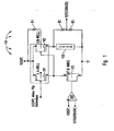
- FIG. 1 illustrates an integrated voltage regulator and reverse voltage protection circuit 100 in accordance with the principles of the present invention.
- the circuit 100 includes two p-channel double-sided extended drain field effect transistors 101 and 102.
- a double-sided extended drain field effect transistor is any field effect transistor in which there is a RESURF region between the drain terminal and the channel region, and another RESURF region between the source terminal and the channel region.
- RESURF REduced SURface Field
- the circuit 100 also includes an n-channel extended drain field effect transistor 103.
- the n-channel extended drain field effect transistor may be an n-channel single-sided extended drain field effect transistor as illustrated in Figure 1 , or may alternatively be an n-channel double-sided extended drain field effect transistor.
- a "single-sided extended drain field effect transistor” means any field effect transistor in which a RESURF region separates only one of the drain or source terminals from the channel region.
- An “extended drain field effect transistor” means either a single-sided or double-sided extended drain field effect transistor.
- the circuit 100 further includes an amplifier 104, and resistors R1, R2 and R3. Although the load 105 that is being protected may be off-circuit, the load 105 may be integrated with the circuit 100.
- the source terminal of the double-sided extended drain field effect transistor 101 is coupled to the voltage supply V(SUP).
- V(SUP) the voltage supply
- two nodes in a circuit are "coupled” if charge may flow from one node to the other during normal operation of the circuit, if even with some resistance.
- the drain terminal of the double-sided extended drain field effect transistor 101 is coupled to the gate terminal of the double-sided extended drain field effect transistor 102.
- the body regions of both double-sided extended drain field effect transistors 101 and 102 are n-wells and are coupled in common and (through the resistor R1) to the supply voltage V(SUP).
- the resistor R1 is a high value resistor that may be composed of, for example, high resistance polysilicon.
- the drain terminal of the n-channel single-sided extended drain field effect transistor 103 is coupled to the drain terminal of the p-channel double-sided extended drain field effect transistor 101.
- the source terminal of the n-channel single-sided extended drain field effect transistor 103 is coupled to a low voltage supply.
- the load 105 is coupled in parallel with the series combination of resistors R2 and R3 between the drain terminal of the p-channel double-sided extended drain field effect transistor 102 and the low voltage supply.
- the p-channel double-sided extended-drain field effect transistor 102 controls current from the supply pin illustrated as having voltage V(SUP) to the load 105.
- the other p-channel double-sided extended-drain field effect transistor 101 is used to bias the gate terminal of the controlling p-channel transistor 102.
- the gate terminal of p-channel transistor 101 is connected to a reference potential generated relative to the supply voltage V(SUP).
- the reference voltage may be the supply voltage V(SUP) minus the threshold voltage Vtp of the p-channel transistor 101. This reference bias limits the current flowing through device 101. Note that there is feedback in that the voltage V(FEEDBACK) is fed back into the lower input terminal of the amplifier 104. If the n-channel single-sided extended drain field effect transistor 103 is turned on by this feedback, the drain current of the p-channel transistor 101 will pull the gate potential of the controlling p-channel transistor 102 below the supply voltage V(SUP) allowing current to flow through the p-channel transistor 102 to the load 105.
- the drain current of the p-channel transistor 101 will raise the gate voltage of the controlling p-channel transistor 102 to the supply voltage V(SUP) shutting off the controlling p-channel transistor 102 so that little, if any current will flow to the load 105.
- the circuit 100 performs voltage regulation when V(SUP) is too high as follows.
- the drain current of the n-channel transistor 103 is controlled by the voltage at the load 105.
- the amplifier 104 reduces the voltage on the n-channel transistor 103 which, in turn, increases the voltage on the gate of controlling p-channel transistor 102 and thereby lowering the current to the load 105.
- the supply voltage V(SUP) is negative with respect to ground.
- the n-Well that represents the body terminal of p-channel transistors 101 and 102 will be forward biased with respect to the P-substrate.
- the high value, current limiting resistor R1 limits the current through the forward biased diodes of all N-Wells connected to V(SUP).
- the circuit 100 includes one amplifier, three transistors, and three resistors. Accordingly, the area consumed by the circuit 100 may be quite small.
- Figure 2 illustrates a cross section of a p-channel double-sided extended-drain field effect transistor 200.
- the transistor 200 may be used for each of the p-channel double-sided extended drain field effect transistors 101 and 102 of Figure 1 , although the transistor 200 represents a unique transistor design that may be useful in any application in which both the source and drain of the transistor may be subject to high reverse bias voltages with respect to the body terminal.
- the double-sided extended drain field effect transistor significantly increases the breakdown voltage at both the source and drain terminals. Accordingly, there is far less likelihood of breakdown occurring in cases in which both the source and drain terminals are subject to high reverse biasing with respect to the body terminal.
- the transistor 200 is fabricated on a p-type substrate 211.
- An n-well 201 is formed in the p-type substrate 211.
- the transistor includes gate terminal 202, source terminal 207 and the drain terminal 204.
- the gate terminal 202 does not laterally extend to either the source terminal 207 or the drain terminal 204, but is laterally spaced from the source terminal 207 and the drain terminal 204.
- a field oxide layer 203B is laterally disposed between the gate terminal 202 and the source terminal 207.
- a field oxide layer 203C is laterally disposed between the gate terminal 202 and the drain terminal 204.
- Other field oxide layers 203A and 203D formed by the same oxide growth and patterning steps as the oxides 203B and 203C may also be present.
- Oxide layer 210 represented by portions 210A, 210B and 210C may overlie the entire structure to provide selective electrical isolation from an upper metal layer.
- a thin oxide resides vertically between the gate terminal 202 and the n-well although the oxide layer is too thin to distinguish in Figure 2 .
- a p-RESURF region 205 is laterally positioned between the drain terminal 204 and the channel region underneath the gate terminal 202 as shown.
- the p-RESURF region 205 operates to electrically connect the drain terminal 204 to the channel region underneath the gate terminal 202.
- the p-RESURF region 205 also serves as a region that may sustain large voltage drops in cases when the voltage at the channel region far exceeds the voltage at the drain terminal 204.
- An additional p-region 206 may be laterally disposed on the other side of the drain terminal 204. Together, the p-RESURF region 205 and the p- region 206 significantly increase the breakdown voltage of the drain terminal 204 with respect to the n-well 201.
- a p-RESURF region 208 is also laterally positioned between the source terminal 207 and the channel region.
- the p-RESURF region 208 performs the same functions for the source terminal 207 as are attributed to the p-RESURF region 205 for the drain terminal 204.
- an additional p- region 209 may be laterally disposed on the other side of the source terminal 207.
- the p- region 209 performs the same functions for the source terminal 207 as are attributed to the p- region 206 for the drain terminal 204.
- a reverse voltage event occurs (e.g., V(SUP) is negative)
- the interface between the n-well 201 and the substrate 211 becomes forward biased. Therefore, the potential of the n-well 201 will be fixed at approximately -0.6V (assuming that the substrate is fixed at ground).
- the drain voltage will drop to approximately ground, while the source voltage will drop to a negative value equal to the negative voltage of V(SUP).
- This negative source voltage is typically greater in magnitude than a standard P+ source to n-well breakdown voltage.
- the breakdown voltage at the interface between the source terminal 207 and the n-well 201 is increased above the magnitude of the reverse voltage. Accordingly, the use of p-RESURF region 208 and p- region 209 isolates the circuit from the negative potential which would damage the circuit under a reverse voltage condition.
- the p-channel double-sided extended drain field effect transistor 200 has high breakdown voltages between the source terminal 207 and the n-well 201, as well as between the drain terminal 204 and the n-well 201.
- the transistor 200 is thus well-suited for applications such as that of Figure 1 in which the drain terminal and source terminals may experience strong reverse biases with respect to the n-well.
- the transistor 200 has been described as a p-channel transistor, a similar n-channel device may also be constructed, using the principles of the present invention, by replacing regions of a first carrier type (e.g., p-type or n-type) of the illustrated transistor 200 with regions of the opposite carrier type (e.g., n-type or p-type).
- a first carrier type e.g., p-type or n-type
- regions of the opposite carrier type e.g., n-type or p-type.
- the fabrication of the transistor 200 may be performed using standard CMOS processes.
- the n-channel single-sided extended drain field effect transistor 103 may be any extended drain field effect transistor including those conventionally available.
- Figure 3 illustrates an n-channel single-sided extended drain field effect transistor 300 that may be used as the n-channel single-sided extended drain field effect transistor 103 of Figure 1 .
- the transistor 300 includes a gate terminal 307, a source terminal 304, a drain terminal 306, and field oxide layer 303 including components 303A, 303B and 303C.
- the source terminal is coupled to the substrate via p+ doped region 305.
- a p-well 301 and n-well 302 are disposed within the substrate as illustrated.
- the transistor 300 may also be fabricated using standard CMOS processes as will be apparent to those of ordinary skill in the art after having reviewed this description and the associated figures.
- the other components 104 and R1, R2 and R3 may also be fabricated using CMOS processes. Accordingly, the entire integrated voltage regulator and reverse voltage protection circuit 100 of Figure 1 may be constructed using standard CMOS processes, and also does not require external circuit components. This reduces the cost of the fabrication. If the load 105 may be fabricated on a chip, then the load 105 may be integrated with the circuit 100 on the same chip. If the load 105 may be fabricated using standard CMOS processes, then the entire circuit 100 with the load 105 may be fabricated using standard CMOS processes.
- FIG. 5 illustrates an integrated overvoltage blocking and reverse voltage protection circuit 500 in accordance with an alternative embodiment of the present invention.
- the elements 501, 502, 503, 504, 505, R51, R52 and R53 may be the same as described above for elements 101, 102, 103, 104, 105, R1, R2 and R3 respectively.
- the voltage divider that includes the series combination of resistors R52 and R53 spans the entire voltage supply rails.
- the element 504 compares the voltage V (DIV) generated by the resistive divider with a reference voltage V(REF). If V(DIV) is lower than V(REF), the voltage supply V(SUP) is considered to be at a safe level and is applied to the load through element 502.
- the circuit 500 would operate to block voltage from reaching the load 505 during an overvoltage condition.
- Figure 6 illustrates an integrated voltage regulator and reverse voltage protection circuit 600 in accordance with another aspect of the present invention.
- the elements 601, 602, 603, 604, 605, R61, R62 and R63 may be the same as described above for elements 101, 102, 103, 104, 105, R1, R2 and R3 respectively.
- the circuit 600 has an additional p-channel extended drain field effect transistor 606 coupled in series between the transistors 601 and 603 as shown.
- the source terminal of the transistor 606 is connected to the gate terminal of the transistor 602. In this configuration, the gate terminal of the transistor 602 is protected from excessively high voltages during an overvoltage condition.
- the modification to Figure 1 shown in Figure 5 may be added to the modification to Figure 1 shown in Figure 6 .
Landscapes
- Semiconductor Integrated Circuits (AREA)
- Metal-Oxide And Bipolar Metal-Oxide Semiconductor Integrated Circuits (AREA)
- Protection Of Static Devices (AREA)
- Emergency Protection Circuit Devices (AREA)
Claims (16)
- Integrierte Spannungsregler- und Gegenspannungsschutzschaltung umfassend:einen ersten Feldeffekttransistor (102, 502) mit doppelseitig verlängertem Drain-Gebiet eines ersten Ladungsträgertyps, der einen Source-Anschluss hat, der mit einer ersten Spannungsquelle verbunden ist;einen zweiten Feldeffekttransistor (101, 501) mit doppelseitig verlängertem Drain-Gebiet des ersten Ladungsträgertyps, der ebenfalls einen Source-Anschluss hat, der mit der ersten Spannungsquelle verbunden ist, und einen Drain-Anschluss hat, der mit einem Gate-Anschluss des ersten Feldeffekttransistors vom ersten Ladungsträgertyp mit doppelseitig verlängertem Drain-Gebiet verbunden ist;einen ersten Widerstand (R1), der zwischen der ersten Versorgungsspannung und einem Substratanschluss des ersten Feldeffekttransistors vom ersten Ladungsträgertyp mit doppelseitig verlängertem Drain-Gebiet und einem Substratanschluss des zweiten Feldeffekttransistors des ersten Ladungsträgertyps mit doppelseitig verlängertem Drain-Gebiet angeordnet ist;einen zweiten Widerstand (R2);einen dritten Widerstand (R3), der mit dem zweiten Widerstand in Serie zwischen einem Drain-Anschluss des ersten Feldeffekttransistors vom ersten Ladungsträgertyp mit doppelseitig verlängertem Drain-Gebiet oder der ersten Spannungsquelle und einer zweiten Spannungsquelle geschaltet ist;einen Feldeffekttransistor (103, 503) mit verlängertem Drain-Gebiet, der von einem zweiten Ladungsträgertyp entgegengesetzt dem ersten Ladungsträgertyp ist, und der einen Drain-Anschluss hat, der mit dem Drain-Anschluss des zweiten Feldeffekttransistors mit doppelseitig verlängertem Drain-Gebiet verbunden ist, und der einen Source-Anschluss hat, der mit der zweiten Spannungsquelle verbunden ist; undeinen Komparator (104, 504), der einen Ausgangsanschluss hat, der mit einem Gate-Anschluss des Feldeffekttransistors vom zweiten Ladungsträgertyp mit verlängertem Drain-Gebiet verbunden ist.
- Schaltung nach Anspruch 1, wobei der Feldeffekttransistor vom zweiten Ladungsträgertyp mit verlängertem Drain-Gebiet ein Feldeffekttransistor vom zweiten Ladungsträgertyp mit einseitig verlängertem Drain-Gebiet ist.
- Schaltung nach Anspruch 1, wobei der Feldeffekttransistor vom zweiten Ladungsträgertyp mit verlängertem Drain-Gebiet ein Feldeffekttransistor vom zweiten Ladungsträgertyp mit doppelseitig verlängertem Drain-Gebiet ist.
- Schaltung nach Anspruch 1, wobei der erste Ladungsträgertyp ein n-Kanaltyp und der zweite Ladungsträgertyp ein p-Kanaltyp ist.
- Schaltung nach Anspruch 1, wobei der erste Ladungsträgertyp ein p-Kanaltyp und der zweite Ladungsträgertyp n-Kanaltyp ist.
- Schaltung nach Anspruch 1, wobei die Schaltung weiterhin eine Lastschaltung umfasst, die zwischen dem Drain-Anschluss des ersten Feldeffekttransistors mit doppel-seitig verlängertem Drain-Gebiet und der zweiten Spannungsquelle angeordnet ist.
- Schaltung nach Anspruch 6, wobei die Schaltung auf einem einzelnen Chip integriert ist.
- Schaltung nach Anspruch 1, wobei ein Knoten zwischen dem zweiten und dem dritten Widerstand mit einem ersten Eingangsanschluss des Komparators verbunden ist.
- Schaltung nach Anspruch 1, wobei ein zweiter Eingangsanschluss des Komparators mit einer Referenzspannung verbindbar ist.
- Schaltung nach Anspruch 9, wobei die Referenzspannung eine erste Referenzspannung ist, wobei ein Gate-Anschluss des zweiten Feldeffekttransistors vom ersten Ladungsträgertyp mit doppelseitig verlängertem Drain-Gebiet mit einer zweiten Spannungsreferenz verbindbar ist.
- Schaltung nach Anspruch 10, wobei die zweite Spannungsreferenz sich von der ersten Spannungsquelle um einen Faktor unterscheidet, der gleich dem absoluten Wert einer Schwellenspannung des zweiten Feldeffekttransistors des ersten Ladungsträgertyps mit doppelseitig verlängertem Drain-Gebiet ist.
- Schaltung nach Anspruch 1, wobei der erste Feldeffekttransistor vom ersten Ladungsträgertyp mit doppelseitig verlängertem Drain-Gebiet Folgendes umfasst:ein Substrat; undeinen Gate-Anschluss, der oberhalb eines Kanalgebiets in dem Substrat liegt, wobei das Substrat weiterhin Folgendes umfasst:ein Drain-Gebiet vom ersten Ladungsträgertyp, wobei das Drain-Gebiet seitlich von dem Kanalgebiet durch ein erstes RESURF-Gebiet vom ersten Ladungsträgertyp getrennt ist; undein Source-Gebiet vom ersten Ladungsträgertyp, wobei das Source-Gebiet seitlich von dem Kanalgebiet durch ein zweites RESURF-Gebiet des ersten Ladungsträgertyps getrennt ist.
- Schaltung nach Anspruch 12, wobei das Substrat weiterhin Folgendes umfasst:ein drittes RESURF-Gebiet vom ersten Ladungsträgertyp, das seitlich so angeordnet ist, dass es an das Drain-Gebiet auf der Seite grenzt, die dem Kanalgebiet abgewandt ist; undein viertes RESURF-Gebiet vom ersten Ladungsträgertyp, das seitlich so angeordnet ist, dass es an das Source-Gebiet auf der Seite grenzt, die dem Kanalgebiet abgewandt ist.
- Schaltung nach Anspruch 1, wobei der erste Feldeffekttransistor vom ersten Ladungsträgertyp mit doppelseitig verlängertem Drain-Gebiet ein erster Feldeffekttransistor vom ersten Ladungsträgertyp mit verlängertem Drain-Gebiet ist, und wobei der zweite Feldeffekttransistor vom ersten Ladungsträgertyp mit doppelseitig verlängertem Drain-Gebiet ein zweiter Feldeffekttransistor vom ersten Ladungsträgertyp mit verlängertem Drain-Gebiet ist, und wobei die Schaltung weiterhin Folgendes umfasst:einen dritten Feldeffekttransistor vom ersten Ladungsträgertyp mit verlängertem Drain-Gebiet, der einen Drain-Anschluss hat, welcher mit dem Drain-Anschluss des Feldeffekttransistors vom zweiten Ladungsträgertyp mit verlängertem Drain-Gebiet verbunden ist, und einen Source-Anschluss hat, der mit dem Drain-Anschluss des zweiten Feldeffekttransistors vom ersten Ladungsträgertyp mit verlängertem Drain-Gebiet und mit dem Gate-Anschluss des ersten Feldeffekttransistors vom ersten Ladungsträgertyp mit verlängertem Drain-Gebiet verbunden ist.
- Schaltung nach einem der Ansprüche 1 bis 14, wobei der Komparator einen Verstärker umfasst.
- Schaltung nach Anspruch 15, wobei ein Knoten zwischen dem ersten und dem zweiten Widerstand mit einem ersten Eingangsanschluss des Verstärkers verbunden ist.
Priority Applications (1)
| Application Number | Priority Date | Filing Date | Title |
|---|---|---|---|
| EP11184888A EP2408010A3 (de) | 2003-07-01 | 2004-05-18 | Feldeffekttransistor mit Drain und Source Offset und integrierte Überspannungsschutz und Sperrspannungsschutz mit einem solchen Transistor |
Applications Claiming Priority (2)
| Application Number | Priority Date | Filing Date | Title |
|---|---|---|---|
| US611714 | 2003-07-01 | ||
| US10/611,714 US6867640B2 (en) | 2003-07-01 | 2003-07-01 | Double-sided extended drain field effect transistor, and integrated overvoltage and reverse voltage protection circuit that uses the same |
Related Child Applications (1)
| Application Number | Title | Priority Date | Filing Date |
|---|---|---|---|
| EP11184888.3 Division-Into | 2011-10-12 |
Publications (3)
| Publication Number | Publication Date |
|---|---|
| EP1494286A2 EP1494286A2 (de) | 2005-01-05 |
| EP1494286A3 EP1494286A3 (de) | 2009-04-01 |
| EP1494286B1 true EP1494286B1 (de) | 2012-12-12 |
Family
ID=33435441
Family Applications (2)
| Application Number | Title | Priority Date | Filing Date |
|---|---|---|---|
| EP04011784A Expired - Lifetime EP1494286B1 (de) | 2003-07-01 | 2004-05-18 | Integrierter Überspannungsschutz und Sperrspannungsschutz mit Feldeffekttransistoren mit Drain- und Source Offset |
| EP11184888A Withdrawn EP2408010A3 (de) | 2003-07-01 | 2004-05-18 | Feldeffekttransistor mit Drain und Source Offset und integrierte Überspannungsschutz und Sperrspannungsschutz mit einem solchen Transistor |
Family Applications After (1)
| Application Number | Title | Priority Date | Filing Date |
|---|---|---|---|
| EP11184888A Withdrawn EP2408010A3 (de) | 2003-07-01 | 2004-05-18 | Feldeffekttransistor mit Drain und Source Offset und integrierte Überspannungsschutz und Sperrspannungsschutz mit einem solchen Transistor |
Country Status (2)
| Country | Link |
|---|---|
| US (2) | US6867640B2 (de) |
| EP (2) | EP1494286B1 (de) |
Families Citing this family (7)
| Publication number | Priority date | Publication date | Assignee | Title |
|---|---|---|---|---|
| US6867640B2 (en) * | 2003-07-01 | 2005-03-15 | Ami Semiconductor, Inc. | Double-sided extended drain field effect transistor, and integrated overvoltage and reverse voltage protection circuit that uses the same |
| US6977491B1 (en) * | 2003-10-06 | 2005-12-20 | National Semiconductor Corporation | Current limiting voltage regulation circuit |
| US7262471B2 (en) * | 2005-01-31 | 2007-08-28 | Texas Instruments Incorporated | Drain extended PMOS transistor with increased breakdown voltage |
| JP2008010667A (ja) * | 2006-06-29 | 2008-01-17 | Mitsumi Electric Co Ltd | 半導体装置 |
| US7724487B2 (en) * | 2008-07-10 | 2010-05-25 | International Business Machines Corporation | Apparatus, system, and method for lossless reverse voltage protection |
| US8115337B2 (en) | 2008-12-01 | 2012-02-14 | Texas Instruments Incorporated | Soft-start circuit |
| EP2632047B1 (de) * | 2012-02-21 | 2014-07-02 | Siemens Aktiengesellschaft | Schutzschaltung und Automatisierungskomponente |
Family Cites Families (21)
| Publication number | Priority date | Publication date | Assignee | Title |
|---|---|---|---|---|
| US4811075A (en) * | 1987-04-24 | 1989-03-07 | Power Integrations, Inc. | High voltage MOS transistors |
| US5047820A (en) * | 1988-09-14 | 1991-09-10 | Micrel, Inc. | Semi self-aligned high voltage P channel FET |
| US5162883A (en) * | 1989-07-04 | 1992-11-10 | Fuji Electric Co., Ltd. | Increased voltage MOS semiconductor device |
| US5517379A (en) * | 1993-05-26 | 1996-05-14 | Siliconix Incorporated | Reverse battery protection device containing power MOSFET |
| US5539610A (en) * | 1993-05-26 | 1996-07-23 | Siliconix Incorporated | Floating drive technique for reverse battery protection |
| US5548147A (en) * | 1994-04-08 | 1996-08-20 | Texas Instruments Incorporated | Extended drain resurf lateral DMOS devices |
| US5498554A (en) * | 1994-04-08 | 1996-03-12 | Texas Instruments Incorporated | Method of making extended drain resurf lateral DMOS devices |
| JP3485655B2 (ja) * | 1994-12-14 | 2004-01-13 | 株式会社ルネサステクノロジ | 複合型mosfet |
| DE19603117A1 (de) * | 1995-02-17 | 1996-08-29 | Int Rectifier Corp | Verpolungs-Schutzschaltung |
| US5781390A (en) * | 1996-12-21 | 1998-07-14 | Sgs-Thomson Microelectronics, Inc. | Integrated supply protection |
| DE19803040A1 (de) * | 1997-01-31 | 1998-08-06 | Int Rectifier Corp | Leistungsschaltung |
| US6043965A (en) * | 1997-11-20 | 2000-03-28 | General Motors Corporation | Low loss reverse battery protection |
| JP3270405B2 (ja) * | 1998-01-26 | 2002-04-02 | セイコーインスツルメンツ株式会社 | 半導体装置 |
| JP3059423B2 (ja) * | 1998-10-19 | 2000-07-04 | 松下電子工業株式会社 | 半導体装置の製造方法 |
| JP4559643B2 (ja) * | 2000-02-29 | 2010-10-13 | セイコーインスツル株式会社 | ボルテージ・レギュレータ、スイッチング・レギュレータ、及びチャージ・ポンプ回路 |
| US6229290B1 (en) * | 2000-05-19 | 2001-05-08 | Silicon Storage Technology, Inc. | Voltage regulating circuit with a clamp up circuit and a clamp down circuit operating in tandem |
| US6522111B2 (en) * | 2001-01-26 | 2003-02-18 | Linfinity Microelectronics | Linear voltage regulator using adaptive biasing |
| EP1280032A1 (de) * | 2001-07-26 | 2003-01-29 | Alcatel | Spannungsregler mit kleiner Verlustspannung |
| US6690147B2 (en) * | 2002-05-23 | 2004-02-10 | Texas Instruments Incorporated | LDO voltage regulator having efficient current frequency compensation |
| EP1439444A1 (de) * | 2003-01-16 | 2004-07-21 | Dialog Semiconductor GmbH | Spannungsregulierungseinrichtung mit kleiner Verlustspannung mit Kaskoden-Struktur |
| US6867640B2 (en) * | 2003-07-01 | 2005-03-15 | Ami Semiconductor, Inc. | Double-sided extended drain field effect transistor, and integrated overvoltage and reverse voltage protection circuit that uses the same |
-
2003
- 2003-07-01 US US10/611,714 patent/US6867640B2/en not_active Expired - Lifetime
-
2004
- 2004-05-18 EP EP04011784A patent/EP1494286B1/de not_active Expired - Lifetime
- 2004-05-18 EP EP11184888A patent/EP2408010A3/de not_active Withdrawn
- 2004-12-13 US US11/010,892 patent/US7279757B1/en not_active Expired - Lifetime
Also Published As
| Publication number | Publication date |
|---|---|
| EP1494286A3 (de) | 2009-04-01 |
| US20050001672A1 (en) | 2005-01-06 |
| EP1494286A2 (de) | 2005-01-05 |
| EP2408010A2 (de) | 2012-01-18 |
| US6867640B2 (en) | 2005-03-15 |
| US7279757B1 (en) | 2007-10-09 |
| EP2408010A3 (de) | 2012-02-22 |
Similar Documents
| Publication | Publication Date | Title |
|---|---|---|
| EP3693994B1 (de) | Schaltung zur steuerung einer gestapelten rückschnappklemme | |
| EP0750793B1 (de) | Siliziumthyristor für esd-schutz | |
| US6690561B2 (en) | Effective gate-driven or gate-coupled ESD protection circuit | |
| US5808342A (en) | Bipolar SCR triggering for ESD protection of high speed bipolar/BiCMOS circuits | |
| US7826238B2 (en) | Power system inhibit method and device and structure therefor | |
| US5543650A (en) | Electrostatic discharge protection circuit employing a mosfet device | |
| US5917336A (en) | Circuit for electrostatic discharge (ESD) protection | |
| EP0535536B1 (de) | Durch Verarmung kontrollierte Isolationsstufe | |
| US5747834A (en) | Adjustable Bipolar SCR holding voltage for ESD protection circuits in high speed Bipolar/BiCMOS circuits | |
| US20070155062A1 (en) | Method and apparatus for controlling a circuit with a high voltage sense device | |
| US5903419A (en) | Circuit for electrostatic discharge (ESD) protection | |
| US20100302810A1 (en) | Voltage converters with integrated low power leaker device and associated methods | |
| US6577480B1 (en) | Adjustable trigger voltage circuit for sub-micrometer silicon IC ESD protection | |
| US20120319177A1 (en) | Junction field effect transistor, integrated circuit for switching power supply, and switching power supply | |
| US6046897A (en) | Segmented bus architecture (SBA) for electrostatic discharge (ESD) protection | |
| JPH11259148A (ja) | 静電放電(esd)保護回路 | |
| JPH11251594A (ja) | 電圧クランプされたゲ―トを有するパワ―mosfet | |
| US5708550A (en) | ESD protection for overvoltage friendly input/output circuits | |
| US6504424B1 (en) | Low voltage metal oxide semiconductor threshold referenced voltage regulator and method of using | |
| US6878996B2 (en) | MOS power transistor | |
| EP1494286B1 (de) | Integrierter Überspannungsschutz und Sperrspannungsschutz mit Feldeffekttransistoren mit Drain- und Source Offset | |
| US7098513B2 (en) | Low trigger voltage, low leakage ESD NFET | |
| US20010033003A1 (en) | Semiconductor device having a protective circuit | |
| EP0785576A2 (de) | Schaltung mit einem Schutzmittel | |
| JPH0553074B2 (de) |
Legal Events
| Date | Code | Title | Description |
|---|---|---|---|
| PUAI | Public reference made under article 153(3) epc to a published international application that has entered the european phase |
Free format text: ORIGINAL CODE: 0009012 |
|
| AK | Designated contracting states |
Kind code of ref document: A2 Designated state(s): AT BE BG CH CY CZ DE DK EE ES FI FR GB GR HU IE IT LI LU MC NL PL PT RO SE SI SK TR |
|
| AX | Request for extension of the european patent |
Extension state: AL HR LT LV MK |
|
| PUAL | Search report despatched |
Free format text: ORIGINAL CODE: 0009013 |
|
| AK | Designated contracting states |
Kind code of ref document: A3 Designated state(s): AT BE BG CH CY CZ DE DK EE ES FI FR GB GR HU IE IT LI LU MC NL PL PT RO SE SI SK TR |
|
| AX | Request for extension of the european patent |
Extension state: AL HR LT LV MK |
|
| 17P | Request for examination filed |
Effective date: 20090928 |
|
| 17Q | First examination report despatched |
Effective date: 20091021 |
|
| AKX | Designation fees paid |
Designated state(s): DE FR IT |
|
| RAP1 | Party data changed (applicant data changed or rights of an application transferred) |
Owner name: SEMICONDUCTOR COMPONENTS INDUSTRIES, LLC |
|
| GRAP | Despatch of communication of intention to grant a patent |
Free format text: ORIGINAL CODE: EPIDOSNIGR1 |
|
| GRAS | Grant fee paid |
Free format text: ORIGINAL CODE: EPIDOSNIGR3 |
|
| GRAA | (expected) grant |
Free format text: ORIGINAL CODE: 0009210 |
|
| AK | Designated contracting states |
Kind code of ref document: B1 Designated state(s): DE FR IT |
|
| REG | Reference to a national code |
Ref country code: DE Ref legal event code: R096 Ref document number: 602004040357 Country of ref document: DE Effective date: 20130207 |
|
| PLBE | No opposition filed within time limit |
Free format text: ORIGINAL CODE: 0009261 |
|
| STAA | Information on the status of an ep patent application or granted ep patent |
Free format text: STATUS: NO OPPOSITION FILED WITHIN TIME LIMIT |
|
| 26N | No opposition filed |
Effective date: 20130913 |
|
| REG | Reference to a national code |
Ref country code: DE Ref legal event code: R097 Ref document number: 602004040357 Country of ref document: DE Effective date: 20130913 |
|
| REG | Reference to a national code |
Ref country code: FR Ref legal event code: PLFP Year of fee payment: 13 |
|
| REG | Reference to a national code |
Ref country code: FR Ref legal event code: PLFP Year of fee payment: 14 |
|
| REG | Reference to a national code |
Ref country code: FR Ref legal event code: PLFP Year of fee payment: 15 |
|
| PGFP | Annual fee paid to national office [announced via postgrant information from national office to epo] |
Ref country code: DE Payment date: 20200421 Year of fee payment: 17 Ref country code: FR Payment date: 20200422 Year of fee payment: 17 |
|
| PGFP | Annual fee paid to national office [announced via postgrant information from national office to epo] |
Ref country code: IT Payment date: 20210422 Year of fee payment: 18 |
|
| REG | Reference to a national code |
Ref country code: DE Ref legal event code: R119 Ref document number: 602004040357 Country of ref document: DE |
|
| PG25 | Lapsed in a contracting state [announced via postgrant information from national office to epo] |
Ref country code: DE Free format text: LAPSE BECAUSE OF NON-PAYMENT OF DUE FEES Effective date: 20211201 |
|
| PG25 | Lapsed in a contracting state [announced via postgrant information from national office to epo] |
Ref country code: FR Free format text: LAPSE BECAUSE OF NON-PAYMENT OF DUE FEES Effective date: 20210531 |
|
| PG25 | Lapsed in a contracting state [announced via postgrant information from national office to epo] |
Ref country code: IT Free format text: LAPSE BECAUSE OF NON-PAYMENT OF DUE FEES Effective date: 20220518 |