EP1493838A1 - Replacement unit and replacement method for substrate in thin-film forming device - Google Patents
Replacement unit and replacement method for substrate in thin-film forming device Download PDFInfo
- Publication number
- EP1493838A1 EP1493838A1 EP03715703A EP03715703A EP1493838A1 EP 1493838 A1 EP1493838 A1 EP 1493838A1 EP 03715703 A EP03715703 A EP 03715703A EP 03715703 A EP03715703 A EP 03715703A EP 1493838 A1 EP1493838 A1 EP 1493838A1
- Authority
- EP
- European Patent Office
- Prior art keywords
- substrate
- carrier
- mask
- stage
- head
- Prior art date
- Legal status (The legal status is an assumption and is not a legal conclusion. Google has not performed a legal analysis and makes no representation as to the accuracy of the status listed.)
- Withdrawn
Links
Images




Classifications
-
- G—PHYSICS
- G11—INFORMATION STORAGE
- G11B—INFORMATION STORAGE BASED ON RELATIVE MOVEMENT BETWEEN RECORD CARRIER AND TRANSDUCER
- G11B7/00—Recording or reproducing by optical means, e.g. recording using a thermal beam of optical radiation by modifying optical properties or the physical structure, reproducing using an optical beam at lower power by sensing optical properties; Record carriers therefor
- G11B7/24—Record carriers characterised by shape, structure or physical properties, or by the selection of the material
- G11B7/26—Apparatus or processes specially adapted for the manufacture of record carriers
-
- G—PHYSICS
- G11—INFORMATION STORAGE
- G11B—INFORMATION STORAGE BASED ON RELATIVE MOVEMENT BETWEEN RECORD CARRIER AND TRANSDUCER
- G11B5/00—Recording by magnetisation or demagnetisation of a record carrier; Reproducing by magnetic means; Record carriers therefor
- G11B5/84—Processes or apparatus specially adapted for manufacturing record carriers
- G11B5/8404—Processes or apparatus specially adapted for manufacturing record carriers manufacturing base layers
-
- C—CHEMISTRY; METALLURGY
- C23—COATING METALLIC MATERIAL; COATING MATERIAL WITH METALLIC MATERIAL; CHEMICAL SURFACE TREATMENT; DIFFUSION TREATMENT OF METALLIC MATERIAL; COATING BY VACUUM EVAPORATION, BY SPUTTERING, BY ION IMPLANTATION OR BY CHEMICAL VAPOUR DEPOSITION, IN GENERAL; INHIBITING CORROSION OF METALLIC MATERIAL OR INCRUSTATION IN GENERAL
- C23C—COATING METALLIC MATERIAL; COATING MATERIAL WITH METALLIC MATERIAL; SURFACE TREATMENT OF METALLIC MATERIAL BY DIFFUSION INTO THE SURFACE, BY CHEMICAL CONVERSION OR SUBSTITUTION; COATING BY VACUUM EVAPORATION, BY SPUTTERING, BY ION IMPLANTATION OR BY CHEMICAL VAPOUR DEPOSITION, IN GENERAL
- C23C14/00—Coating by vacuum evaporation, by sputtering or by ion implantation of the coating forming material
- C23C14/22—Coating by vacuum evaporation, by sputtering or by ion implantation of the coating forming material characterised by the process of coating
- C23C14/50—Substrate holders
-
- C—CHEMISTRY; METALLURGY
- C23—COATING METALLIC MATERIAL; COATING MATERIAL WITH METALLIC MATERIAL; CHEMICAL SURFACE TREATMENT; DIFFUSION TREATMENT OF METALLIC MATERIAL; COATING BY VACUUM EVAPORATION, BY SPUTTERING, BY ION IMPLANTATION OR BY CHEMICAL VAPOUR DEPOSITION, IN GENERAL; INHIBITING CORROSION OF METALLIC MATERIAL OR INCRUSTATION IN GENERAL
- C23C—COATING METALLIC MATERIAL; COATING MATERIAL WITH METALLIC MATERIAL; SURFACE TREATMENT OF METALLIC MATERIAL BY DIFFUSION INTO THE SURFACE, BY CHEMICAL CONVERSION OR SUBSTITUTION; COATING BY VACUUM EVAPORATION, BY SPUTTERING, BY ION IMPLANTATION OR BY CHEMICAL VAPOUR DEPOSITION, IN GENERAL
- C23C14/00—Coating by vacuum evaporation, by sputtering or by ion implantation of the coating forming material
- C23C14/22—Coating by vacuum evaporation, by sputtering or by ion implantation of the coating forming material characterised by the process of coating
- C23C14/56—Apparatus specially adapted for continuous coating; Arrangements for maintaining the vacuum, e.g. vacuum locks
-
- G—PHYSICS
- G11—INFORMATION STORAGE
- G11B—INFORMATION STORAGE BASED ON RELATIVE MOVEMENT BETWEEN RECORD CARRIER AND TRANSDUCER
- G11B7/00—Recording or reproducing by optical means, e.g. recording using a thermal beam of optical radiation by modifying optical properties or the physical structure, reproducing using an optical beam at lower power by sensing optical properties; Record carriers therefor
- G11B7/24—Record carriers characterised by shape, structure or physical properties, or by the selection of the material
- G11B7/26—Apparatus or processes specially adapted for the manufacture of record carriers
- G11B7/265—Apparatus for the mass production of optical record carriers, e.g. complete production stations, transport systems
-
- G—PHYSICS
- G11—INFORMATION STORAGE
- G11B—INFORMATION STORAGE BASED ON RELATIVE MOVEMENT BETWEEN RECORD CARRIER AND TRANSDUCER
- G11B7/00—Recording or reproducing by optical means, e.g. recording using a thermal beam of optical radiation by modifying optical properties or the physical structure, reproducing using an optical beam at lower power by sensing optical properties; Record carriers therefor
- G11B7/24—Record carriers characterised by shape, structure or physical properties, or by the selection of the material
- G11B7/26—Apparatus or processes specially adapted for the manufacture of record carriers
- G11B7/266—Sputtering or spin-coating layers
-
- H—ELECTRICITY
- H10—SEMICONDUCTOR DEVICES; ELECTRIC SOLID-STATE DEVICES NOT OTHERWISE PROVIDED FOR
- H10P—GENERIC PROCESSES OR APPARATUS FOR THE MANUFACTURE OR TREATMENT OF DEVICES COVERED BY CLASS H10
- H10P72/00—Handling or holding of wafers, substrates or devices during manufacture or treatment thereof
- H10P72/50—Handling or holding of wafers, substrates or devices during manufacture or treatment thereof for positioning, orientation or alignment
-
- G—PHYSICS
- G11—INFORMATION STORAGE
- G11B—INFORMATION STORAGE BASED ON RELATIVE MOVEMENT BETWEEN RECORD CARRIER AND TRANSDUCER
- G11B11/00—Recording on or reproducing from the same record carrier wherein for these two operations the methods are covered by different main groups of groups G11B3/00 - G11B7/00 or by different subgroups of group G11B9/00; Record carriers therefor
- G11B11/10—Recording on or reproducing from the same record carrier wherein for these two operations the methods are covered by different main groups of groups G11B3/00 - G11B7/00 or by different subgroups of group G11B9/00; Record carriers therefor using recording by magnetic means or other means for magnetisation or demagnetisation of a record carrier, e.g. light induced spin magnetisation; Demagnetisation by thermal or stress means in the presence or not of an orienting magnetic field
- G11B11/105—Recording on or reproducing from the same record carrier wherein for these two operations the methods are covered by different main groups of groups G11B3/00 - G11B7/00 or by different subgroups of group G11B9/00; Record carriers therefor using recording by magnetic means or other means for magnetisation or demagnetisation of a record carrier, e.g. light induced spin magnetisation; Demagnetisation by thermal or stress means in the presence or not of an orienting magnetic field using a beam of light or a magnetic field for recording by change of magnetisation and a beam of light for reproducing, i.e. magneto-optical, e.g. light-induced thermomagnetic recording, spin magnetisation recording, Kerr or Faraday effect reproducing
- G11B11/10582—Record carriers characterised by the selection of the material or by the structure or form
Definitions
- the present invention relates to a substrate replacing unit that performs supply and receipt of a substrate for a thin film forming device and method for replacing a substrate. More specifically, the present invention relates to a substrate replacing unit that receives a substrate on which a film has been already formed and the like from, and supplies a new substrate to, a thin film forming device, e.g., sputtering device, and method of receiving and supplying a substrate.
- a thin film forming device e.g., sputtering device
- CD-based disks e.g., CD, CD-R and CD-RW
- optical disks including DVD-based disks, e.g., DVD-ROM and DVD-R
- magneto-optical disks e.g., MO and MD.
- These disks are produced by providing thin films on a substrate, e.g., that of polycarbonate, by a varying method, e.g., sputtering or spin coating.
- the substrate is normally provided with a through-hole at the center for ease of substrate handling, e.g., for mounting a drive thereon.
- a thin metallic film e.g., that for a reflective film
- a thin metallic film is formed by sputtering, where a disk-like substrate is fixed and held to face a target in a vacuum chamber, kept at a given pressure by a gas for discharging, e.g., argon.
- a voltage is applied to the target. This generates a discharge between the target and substrate to produce a plasma, and the ions in the plasma sputters the target constituting element on the target surface onto the substrate.
- the sputtered particles are deposited on the substrate to form a film thereon.
- a sputtering device for the above case is of the so-called multi-target type, which is provided with a plurality of film forming chambers arranged in a circle with a robot at the center for supplying substrates one by one to the chambers to be coated with a thin film therein.
- An optical disk or the like needs regions on which no film is formed, e.g., periphery around the hole at the center and periphery around the substrate. Therefore, the substrate is covered with jigs called an inner mask and outer mask on these regions during sputtering to form a thin film.
- an outer mask or the like is fixed on a substrate, and the substrate assembly is transferred to or from each film forming device or film forming chamber in a multi-target sputtering device. More specifically, in a multi-target sputtering device, an assembly of substrate and masks held and fixed on a holding jig called carrier is transferred to or from each film forming chamber.
- An optical disk or the like may be coated with a non-metallic film, e.g., that of oxide or nitride, as a protective film, which is formed by sputtering with a target of oxide or nitride.
- a non-metallic film e.g., that of oxide or nitride
- An oxide or nitride target generally needs a higher voltage for generating or maintaining a discharge, and a lower film forming speed to produce a film of good properties. Therefore, it takes a longer time to have a film of given thickness and exposes the substrate to a high-density plasma for a longer time, accordingly.
- a substrate for an optical disk or the like is generally made of polycarbonate or the like, which is low in resistance to heat. Therefore, the substrate should be kept at its heat-resistance temperature or lower even during the film forming process by sputtering.
- the substrate When coated with an oxide film by plasma-aided sputtering, the substrate may be easily heated to its heat-resistance temperature or higher by radiation heat from the plasma, energy of the sputtered particles hitting the substrate or the like, because it is exposed to a high-density plasma for a longer film forming time.
- One of the countermeasures against these problems is use of a carrier of higher heat capacity, to absorb part of thermal energy which would be otherwise directly transferred to the substrate in contact with the carrier, and thereby to retard time required for increasing substrate temperature.
- Another countermeasure is forming an oxide film or the like not in a single film forming chamber but in a plurality of chambers to take a longer time with inter-chamber cooling to control substrate temperature rise. In this case, however, the substrate may be eventually heated to its heat-resistance temperature or higher by heat from the carrier, when a quantity of heat accumulated in the carrier exceeds a certain level.
- the temperature rise may be controlled by a treatment chamber dedicated for cooling between the film forming chambers.
- This concept is inefficient for cooling a carrier itself, because of lack of heat-transferring media, e.g., air, around the carrier in a vacuum chamber with the result that heat accumulated in the carrier cannot be easily released.
- increasing number of film forming or cooling chambers may increase film forming time to deteriorate treatment efficiency.
- the substrate replacing unit of the present invention which can solve the above problems, transfers, between carrier holders in a film forming device, a substrate, mask of a magnetic material for covering a given part on the substrate and carrier comprising a magnetic material which holds the substrate and mask and is held by the carrier holder, wherein the unit comprises a substrate replacing hand equipped with a carrier attaching/detaching means for receiving the carrier on which the substrate and mask are mounted from the carrier holder and for holding the substrate, mask and carrier; head facing the substrate replacing hand for transferring the substrate, mask and carrier by a magnetic force between itself and the hand; mask fixing means for fixing the mask thereon; stage facing the head at a position different from that of the substrate replacing hand for transferring the mask and substrate between itself and head by the mask fixing means; and stand-by position located between the substrate replacing hand and stage, at which the carrier held by the head is cooled after it transfers the substrate and mask to the stage.
- the carrier attaching/detaching means in the substrate replacing hand for the substrate replacing unit works in concert with carrier attaching/detaching holes provided in the carrier to pass therethrough, each being composed of an elongate through-hole of a given width and smaller diameter and circular through-hole of larger diameter.
- the substrate replacing hand is preferably composed of a substrate fixing member and carrier fixing pins, the substrate fixing member working to fix the substrate, mask and carrier, and being rotatable in the direction perpendicular to the substrate, and each of the carrier fixing pins being provided at a position corresponding to that of one of the carrier attaching/detaching holes in the substrate fixing member, and composed of a smaller-diameter section and larger-diameter section provided at the end of the smaller-diameter section, the former having a diameter to allow the smaller-diameter hole of the carrier fixing hole to be fit and longer than the depth of the smaller-diameter hole of the carrier fixing hole while the latter having a diameter to allow the larger-diameter hole of the fixing hole to be fit but not to allow the smaller-diameter hole to be fit.
- the present invention also provides another substrate replacing unit which can solve the above problems. It replaces, between carrier holders in a film forming device, a film-coated and uncoated substrate with each other together with a mask for covering a given part on the substrate and carrier which holds the substrate and mask and is held by the carrier holder, wherein the unit comprises a substrate replacing hand which replaces, between the carrier holders, the film-coated and uncoated substrate with each other together with the mask and carrier; stage on which the film-coated or uncoated substrate and mask are set; and arm head which receives the film-coated substrate, mask and carrier from the substrate replacing hand, transfers the film-coated substrate and mask to the stage, stands by for a given time while holding the carrier, and then receives the uncoated substrate and mask from the stage.
- the unit comprises a substrate replacing hand which replaces, between the carrier holders, the film-coated and uncoated substrate with each other together with the mask and carrier; stage on which the film-coated or uncoated substrate and mask are set; and arm
- the method of the present invention for replacing a substrate which can solve the above problems, replaces, between carrier holders in a film forming device, a substrate, mask of a magnetic material for covering a given part on the substrate and carrier comprising a magnetic material which holds the substrate and mask and is held by the carrier holder, comprising a step of receiving the substrate, mask and carrier from the carrier holder by a substrate replacing hand; step of receiving the substrate, mask and carrier from the substrate replacing hand by an arm head; step of setting the substrate and mask received by the arm head on a stage; step of replacing the substrate and mask by a new substrate and mask on the stage; step of transferring the new substrate and mask together with the carrier which holds them to the substrate replacing hand by the arm head; and step of transferring the new substrate and mask together with the carrier which holds them to the carrier holder by the substrate replacing hand, wherein the carrier held by the arm head is cooled while the substrate and mask are replaced on the stage.
- FIG. 1 presents a top view outlining structure of the substrate replacing unit of one embodiment of the present invention and sputtering device.
- the sputtering device 100 having 14 chambers, 13 film forming chambers 102 and one substrate charging/discharging chamber 103.
- Each film forming chamber 102 located on each side of the tetradecagon is composed of various structures, e.g., those for limiting a discharge space to a specific region, e.g., in the vicinity of target (the so-called earth shield structure), for preventing the excess sputtered particles from being deposited in the unit inside (the so-called deposition shield structure), for introducing argon gas or the like for discharging, and for vacuum exhaust.
- these structures are not directly related to this invention, and their diagrammatic representation and description are omitted.
- the carrier holding/transferring unit 105 is provided at the center of the circumference on which the film forming chambers 102 are located. It is equipped with the 14 carrier holders 70 radiating from the rotational center of the carrier holding/transferring unit 105, each simultaneously holding the substrate 1, mask 2 and carrier 10.
- the carrier 10 can be handled independently from the carrier holder 70 in the present invention. Each carrier holder 70 is facing each film forming chamber 102, while being rotated by the carrier holding/transferring unit 105.
- the device shown in FIG. 1 rotates the carrier holders 70 clockwise to form thin films one by one on the substrates, where each of these holders 70 receives the substrate 1, mask 2 and carrier 10 at the substrate charging/discharging chamber. 103 while stopping in front of the film forming chamber 102 for a given time.
- the substrate 1 has moved past the 13 film forming chambers 102 to complete the film forming step in the device 100, it is withdrawn together with the mask 2 and carrier 10 from the substrate charging/discharging chamber 103.
- the substrate replacing unit 6, positioned in front of the substrate charging/discharging chamber 103 receives the film-coated substrate 1 from the carrier holder 70 together with the mask 2 and carrier 10 by the substrate replacing hand 20.
- the substrate replacing unit 6 is composed of the substrate replacing hand 20, first and second arm heads 30 and 40, and first and second stages 50 and 60.
- the first and second arm heads 30 and 40 have the first and second heads 31 and 41, respectively, at the front ends, and are connected to each other at a contained angle of around 90° at the other ends. They are supported by an arm head driving mechanism (not shown) in such a way that they can rotate around the connection.
- the first and second stages 50 and 60 are arranged to be 180° symmetrical to each other around the connection, and apart from the connection at the same distance as that between the connection and head 31 (or 41) center.
- the substrate replacing hand 20, described later, is positioned at the midpoint between the first and second stages 50 and 60 on the same plane, and apart from the rotational center at the same distance as that between the connection center and head 31 (or 41) center.
- the first and second heads 31 and 41 are positioned at the midpoint between the first stage 50 and substrate replacing hand 20 and between the second stage 60 and substrate replacing hand 20, respectively, on the same plane.
- This design allows the second head 41 to be on the substrate replacing hand 20 on the same plane when the first head 31 is on the first stage 50, and similarly the first head 31 to be on the substrate replacing hand 20 on the same plane when the second head 41 is on the second stage 60.
- FIG. 2 which is a front view of the carrier 10
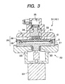
- FIG. 3 which is a cross-sectional view illustrating the substrate 1, mask 2 and carrier 10 transferred between the substrate replacing hand 20 and first or second arm head 30 or 40
- FIG. 4 which is a cross-sectional view illustrating the substrate 1, mask 2 and carrier 10 transferred between the carrier holder 70 and substrate replacing hand 20
- FIG. 5 which is a cross-sectional view illustrating the substrate 1 and mask 2 held by the first or second stage 50 or 60
- FIG. 6 which is a cross-sectional view illustrating the carrier 10 held by the first or second arm head 30 or 40 for reference.
- the substrate 1 in this embodiment has no through-hole at the center and needs no inner mask, accordingly.
- the carrier 10 is provided with a circularly arranged groove 11 on the substrate supporting surface to hold the projection 3 on the back side of the outer mask 2, and also with small magnets 12 arranged on the basal plane of the groove 11.
- the carrier fixing through-holes 13 and carrier attaching/detaching through-holes 14 are arranged around the outer periphery of the circularly arranged groove 11 at the same distance from the carrier center.
- Each of these carrier fixing through-holes 13 and carrier attaching/detaching through-holes 14 is composed of the circumferentially extending elongate through-hole 15 of smaller diameter and circular through-hole 16 of larger diameter, connected to each other at the ends to form the continuous hole.
- the carrier fixing through-holes 13 are positioned 90° apart from each other, and each of the carrier attaching/detaching through-holes 14 is positioned at the midpoint between the carrier fixing through-holes 13.
- These holes 13 and 14 are positioned in such a way that the position of the elongate hole relative to the circular hole 16 alternates along the circumference.
- the substrate charging/discharging chamber 103 is purged with dried nitrogen gas or the like while it is containing the substrate 1, before being open to the air.
- the substrate 1, mask 2 and carrier 10 are supported by the carrier holder 70 in the sputtering device 100, as illustrated in FIG. 4.
- the carrier fixing member 71 in the carrier holder 70 is connected to the motor 72, by which it is driven to rotate while being supported by the bearings 73.
- the mask 2 is fast held and fixed on the carrier 10 magnetically by the small magnets 12 provided in the carrier 10.
- the almost circular substrate 1 is held by the carrier 10 while being placed between the mask 2 and carrier 10.
- the carrier holder 70 has a magnet (not shown) and carrier fixing pins 74 provided in the carrier fixing member 71 and arranged to correspond to the respective carrier fixing holes 13.
- Each of the carrier fixing pins 74 is composed of a smaller-diameter section 75 and larger-diameter section 76 provided at the end of the smaller-diameter section, the former having a diameter to allow the smaller-diameter hole 15 of the carrier fixing hole 13 to be fit and longer than depth of the smaller-diameter hole 15 of the carrier fixing hole 13 while the latter having a diameter to allow the larger-diameter hole 16 of the fixing hole 13 to be fit but not to allow the smaller-diameter hole 15 to be fit.
- the length of the smaller-diameter section 75 of the carrier fixing pin 74 is set so as to be larger than the depth of the smaller-diameter hole 15 of the carrier fixing hole 13.
- the mask 2 and carrier 10 are magnetically held by the carrier holder 70 by a magnet (not shown).
- the fixing pin 74 is fit into the larger-diameter hole 16 of the carrier fixing hole 13, and is then rotated together with the carrier fixing member 71 by the carrier holder rotating motor 72 towards the smaller-diameter hole 15 of the carrier fixing hole 13. This fits the larger-diameter section 76 of the carrier fixing pin 74 into the smaller-diameter hole 15 of the carrier fixing hole 13 to fix the carrier 10 on the carrier holder 70.
- the substrate replacing hand 20 has the carrier supporting member 21, connected to the carrier attaching/detaching motor 22, by which it is driven to rotate while being supported by the bearings 23.
- the carrier supporting member 21 fixes and holds the carrier 10 on the carrier supporting plane, which is provided with the carrier attaching/detaching pins 24, each being arranged at a position to correspond to the carrier attaching/detaching hole 14 provided in the carrier 10 and having the same shape as the carrier fixing pin 74, described earlier.
- the carrier attaching/detaching pin 24 is composed of the smaller-diameter section 25 and larger-diameter section 26 provided at the end of the section 25, the former being longer than depth of the smaller-diameter hole 15 of the carrier attaching/detaching hole 14.
- These carrier attaching/detaching pins 24 constitute the carrier attaching/detaching means which works in concert with the corresponding carrier attaching/detaching holes 14.
- the substrate replacing hand 20 moves closer to the carrier holder 70 holding the substrate 1 and the like to fit each of the carrier attaching/detaching pins 24 into the corresponding larger-diameter hole 16 of the carrier attaching/detaching hole 14.
- the carrier attaching/detaching rotating motor 22 rotates the carrier attaching/detaching pin 24 fit into the larger-diameter hole 16 towards the smaller-diameter hole 15 to fix the carrier 10 on the substrate replacing hand 20.
- the carrier holder rotating motor 72 rotates the carrier fixing pin 74 together with the carrier fixing section 71 towards the larger-diameter hole 16 of the carrier fixing hole 13. This allows the substrate 1, mask 2 and carrier 10 to be detached from the carrier holder 70, completing transfer of the substrate 1 and the like from the carrier holder 70 to the substrate replacing hand 20. Then, the substrate replacing hand 20 is driven back by a substrate replacing hand driving mechanism (not shown) to change the vertical attitude which almost vertically supports the substrate 1 facing the carrier holder 70 to the horizontal attitude which almost horizontally supports the substrate 1 from the above.
- the first and second arm heads 30 and 40 are standing by at the respective stand-by position 80 while the substrate replacing hand 20 is changing its attitude to the horizontal one after receiving the substrate 1, the mask 2 and carrier 10 from the carrier holder 70.
- the carrier 10 to be transferred to the carrier holder 70 is being held by the first head 31 of the first arm head 30 (the condition shown in FIG. 6) and cooled by nitrogen gas or the like at the corresponding stand-by position 80, while the second head 41 of the second arm head 40 is standing by at the corresponding stand-by position 80 without holding the carrier 10 or the like to wait ready for receiving the film-coated substrate 1 and the like.
- the uncoated substrate 1 is waiting on the first stage 50 (the condition shown in FIG. 5) to be received by the carrier 10 held by the first head 31.
- the uncoated substrate 1 on which the mask 2 is mounted is placed on the first stage 50 with the surface to be film-coated facing downwards (facing the stage surface).
- the stage 50 has the stage magnets 52 inside, supported by the stage magnet arm 53 connected to the stage air cylinder 54. These stage magnets 52, magnet arm 53 and air cylinder 54 constitute the mask fixing means.
- stage magnets 52 are driven by the stage air cylinder 54 to move between the nearest and farthest positions from the mask supporting plane 51 (stage surface), while being supported by the stage magnet arm 53.
- the outer mask 2 of a magnetic material is fixed and held on the stage surface, when the stage magnet 52 moves to the nearest position to the surface 51 (the condition shown in FIG. 5), which is accompanied by the substrate 1 being held at the given position corresponding to the mask 2 position.
- each of the first and second heads 31 and 41 has the head magnet 33 inside, which is supported by the head magnet arm 34 connected to the head air cylinder 35.
- the head magnet 33 is driven by the cylinder 35 to move between the nearest and farthest positions from the carrier supporting plane 32 in the head 31, while being supported by the head magnet arm 34.
- the carrier 10 with the small magnets 12 inside is magnetically fixed and held on the carrier supporting plane 32 by the small magnets 12, when the head magnet 33 moves to the nearest position to the carrier supporting plane 32 (the condition shown in FIG. 6). This condition represents the first head 31 standing by at present.
- the first and second arm heads 30 and 40 rotate around the connection by the arm head driving mechanism (not shown), and stop when the first head 31 reaches over the first stage 50 and the second head 41 over the substrate replacing hand 20 in the horizontal position. Then, the head 31 is moved downwards to the first stage 50, and the head 41 to the carrier supporting member 21 of the substrate replacing hand 20 in the horizontal position. These heads stop, when the carrier 10 held by the first head 31 comes into contact with the mask 2 and substrate 1 on the first stage 50, and, at the same time, the second head 41 comes into contact with the carrier 10 held by the substrate replacing hand 20. The contact conditions are confirmed by a common touch sensor (not shown).
- the stage air cylinder 54 drives the stage magnets 52 to the farthest position from the first stage 50 surface. Therefore, the magnetic force by the magnets 52 on the mask 2 becomes smaller than the combined magnetic force on the mask 2 by the small magnets 12 in the carrier and head magnet 33 in the first head 31, with the result that the substrate 1 and mask 2 fast adhere to the carrier 10. They are as a unit held by the first head 31.
- the second head 41 descends without holding the carrier 10 and the like, together with the first head 31, and stops when its carrier supporting member 21 comes into contact with the back side of the carrier 10 supported by the substrate replacing hand 20.
- the head air cylinder 35 drives the head magnet 33 to the nearest position from the carrier supporting plane 32, which magnetically attracts the substrate 1, and mask 2 and carrier 10 holding the substrate 1 in-between.
- the carrier attaching/detaching rotating motor 22 rotates the carrier supporting member 21 and carrier attaching/detaching pins 24 in the substrate replacing hand 20, to release the carrier attaching/detaching pins 24 from the corresponding carrier attaching/detaching holes 14.
- the first head 31 holds the uncoated substrate 1, and mask 2 and carrier 10 holding the substrate 1 in-between
- the second head 41 holds the film-coated substrate 1, and mask 2 and carrier 10 holding the film-coated substrate 1 in-between.
- the arm head driving mechanism (not shown) moves the first and second arm heads 30 and 40 upwards to a given height, and rotate them until the first head 31 reaches over the substrate replacing hand 20 and the second head 41 over the second stage 60.
- the first and second arm heads 30 and 40 descend until the carrier attaching/detaching pins 24 in the substrate replacing hand 20 are fit into the corresponding carrier attaching/detaching holes 14 in the carrier 10 held by the first head 31.
- the mask 2 held by the second head 41 comes into contact with the mask supporting plane 51 in the second stage 60.
- the carrier supporting member 21 in the substrate replacing hand 20 and carrier attaching/detaching pins 24 are rotated by the carrier attaching/detaching rotating motor 22 to move.
- the head air cylinder 35 drives the head magnet 33 in the first head 31 to the farthest position from the carrier supporting plane 32 in the first head 31. This transfers the substrate 1 and the like from the first head 31 to the substrate replacing hand 20, and, at the same time, the mask 2 and substrate 1 from the second head 41 to the second stage 60.
- the second stage 60 has the same structure as the first stage 50 described earlier.
- the stage air cylinder 54 drives the stage magnet 52 held by the stage magnet arm 53 in the second stage 60 to the nearest position from the mask supporting plane 51 as the stage surface.
- the combined magnetic force on the mask 2 by the head magnet 33 in the second head 41 and the small magnets 12 in the carrier 10 being held by the head 41 becomes smaller than the magnetic force on the mask 2 by the stage magnets 52.
- the head magnet 33 is designed to have a stronger magnetic force than the stage magnets 52 on the small magnets 12 in the carrier 10. Therefore, the substrate 1 and mask 2 are magnetically held by the stage 60, and the carrier 10 by the head 41 as the second head 41 ascends.
- the arm head driving mechanism rotates the first and second arm heads 30 and 40 to move to the respective stand-by position 80.
- the substrate 1, mask 2 and carrier 10 are transferred from the substrate replacing hand 20 to the carrier holder 70, i.e., the order of the above procedure is reversed.
- the film-coated substrate 1 and mask 2 set on the second stage 60 are replaced by the uncoated substrate 1 and mask 2 by a substrate transferring robot (not shown).
- the charging/discharging chamber which contains the carrier holder 70 holding the uncoated substrate 1 and the like, is exhausted, to start the film forming process for the substrate 1.
- the film-coated substrate 1, mask 2 and the carrier 10 holding them are transferred, while being supported by the carrier holder 70, to the substrate charging/discharging chamber 103, which is then open to the air.
- the conditions in which the second stage 60 supports the uncoated substrate 1 and mask 2, the second head 41 holds the carrier 10, the first stage 50 and first head 31 support nothing are the same as those described above for transferring the substrate 1, mask 2 and carrier 10, except that each stage and head are replaced. Transfer of the substrate is repeated in the same manner as in the above procedure, except that each stage and head are replaced.
- the above-described substrate transfer procedure allows the carrier held by the head to be cooled in a natural or forced manner while it is at the stand-by position. This allows a thin film to be formed by sputtering on a substrate set on a carrier which is kept controlled at a constant temperature or a given temperature or lower. It is therefore possible to control substrate temperature rise by use of a carrier of adequate heat capacity, even when a film forming process which exposes a substrate to a plasma for a certain time or longer is needed.
- This embodiment forms a film on a substrate having no through-hole at the center.
- the present invention is not limited to such a substrate, and also applicable to a substrate with a through-hole at the center.
- this embodiment depends on a magnetic force for fixing a mask on a stage.
- various other fixing means e.g., fixing under a vacuum
- this embodiment uses attaching/detaching pins for carrier attaching/detaching.
- various other fixing means e.g., fixing under a vacuum, may be also used for the above purpose.
- a mask for covering the substrate center, the so-called inner mask may be additionally used.
- the inner mask may be magnetically fixed on the substrate by one or more magnets provided within the carrier. The magnet may be separately provided for the above purpose.
- this embodiment transfers a substrate and the like by a substrate replacing hand, arm head and stage while they are kept horizontal. However, they may be transferred while being kept almost vertical. Still more, this embodiment cools a carrier with dried nitrogen or the like at a stand-by position.
- the cooling method is not limited to this.
- a plate-shape cooling mechanism or the like cooled with water or the like may be placed underneath a head at a stand-by position, where it is pressed to the carrier in the air, or carrier temperature may be controlled by a water-cooling mechanism or the like provided in the head itself.
- this embodiment employs a sputtering device for forming thin films.
- the film may be formed by various other devices, e.g., evaporator, CVD device or the like.
- the present invention is applicable not only to optical disks but also to other products whose central part is removed later, e.g., all types of disk-like members including hard disks.
- the present invention allows a substrate and the like to be held by a carrier whose temperature is kept at a constant level or a given level or lower. Therefore, it can widen conditions for forming a thin film on a substrate, because heat energy given to a substrate can be released to a cooled carrier, even when a film forming process which exposes a substrate to a plasma for a long time is adopted.
Landscapes
- Engineering & Computer Science (AREA)
- Chemical & Material Sciences (AREA)
- Manufacturing & Machinery (AREA)
- Chemical Kinetics & Catalysis (AREA)
- Materials Engineering (AREA)
- Mechanical Engineering (AREA)
- Metallurgy (AREA)
- Organic Chemistry (AREA)
- Physical Vapour Deposition (AREA)
- Container, Conveyance, Adherence, Positioning, Of Wafer (AREA)
- Manufacturing Optical Record Carriers (AREA)
Abstract
The present invention receives a film-coated
substrate together with a carrier from a substrate
replacing head which receives the substrate and
carrier from a film forming device, while the
substrate is transferred between the substrate
replacing head and a stage on which the substrate is
to be set; transfers only the substrate to the stage
while the carrier is held; cools the carrier while it
is held; then receives an uncoated substrate set on
the stage by the carrier being held; and transfers
the substrate and carrier to the film forming device
by the substrate replacing head. This structure
prevents temperature rise at the substrate being
coated with a film to allow control of carrier
temperature for a thin film forming process which
uses a carrier for holding the substrate.
Description
- The present invention relates to a substrate replacing unit that performs supply and receipt of a substrate for a thin film forming device and method for replacing a substrate. More specifically, the present invention relates to a substrate replacing unit that receives a substrate on which a film has been already formed and the like from, and supplies a new substrate to, a thin film forming device, e.g., sputtering device, and method of receiving and supplying a substrate.
- Various types of disks have been developed with a circular substrate which supports a recording medium, in particular that having a disk shape. These include CD-based disks, e.g., CD, CD-R and CD-RW; optical disks including DVD-based disks, e.g., DVD-ROM and DVD-R; and magneto-optical disks, e.g., MO and MD.
- These disks are produced by providing thin films on a substrate, e.g., that of polycarbonate, by a varying method, e.g., sputtering or spin coating. The substrate is normally provided with a through-hole at the center for ease of substrate handling, e.g., for mounting a drive thereon.
- Of thin films to be formed, a thin metallic film, e.g., that for a reflective film, is formed by sputtering, where a disk-like substrate is fixed and held to face a target in a vacuum chamber, kept at a given pressure by a gas for discharging, e.g., argon. In general, in this state, a voltage is applied to the target. This generates a discharge between the target and substrate to produce a plasma, and the ions in the plasma sputters the target constituting element on the target surface onto the substrate. The sputtered particles are deposited on the substrate to form a film thereon.
- Some disks need a plurality of thin films to be formed by a sputtering device, depending on its film structure. A sputtering device for the above case is of the so-called multi-target type, which is provided with a plurality of film forming chambers arranged in a circle with a robot at the center for supplying substrates one by one to the chambers to be coated with a thin film therein. An optical disk or the like needs regions on which no film is formed, e.g., periphery around the hole at the center and periphery around the substrate. Therefore, the substrate is covered with jigs called an inner mask and outer mask on these regions during sputtering to form a thin film.
- In a conventional sputtering device, therefore, an outer mask or the like is fixed on a substrate, and the substrate assembly is transferred to or from each film forming device or film forming chamber in a multi-target sputtering device. More specifically, in a multi-target sputtering device, an assembly of substrate and masks held and fixed on a holding jig called carrier is transferred to or from each film forming chamber.
- An optical disk or the like may be coated with a non-metallic film, e.g., that of oxide or nitride, as a protective film, which is formed by sputtering with a target of oxide or nitride. An oxide or nitride target, however, generally needs a higher voltage for generating or maintaining a discharge, and a lower film forming speed to produce a film of good properties. Therefore, it takes a longer time to have a film of given thickness and exposes the substrate to a high-density plasma for a longer time, accordingly.
- A substrate for an optical disk or the like is generally made of polycarbonate or the like, which is low in resistance to heat. Therefore, the substrate should be kept at its heat-resistance temperature or lower even during the film forming process by sputtering. When coated with an oxide film by plasma-aided sputtering, the substrate may be easily heated to its heat-resistance temperature or higher by radiation heat from the plasma, energy of the sputtered particles hitting the substrate or the like, because it is exposed to a high-density plasma for a longer film forming time.
- One of the countermeasures against these problems is use of a carrier of higher heat capacity, to absorb part of thermal energy which would be otherwise directly transferred to the substrate in contact with the carrier, and thereby to retard time required for increasing substrate temperature. Another countermeasure is forming an oxide film or the like not in a single film forming chamber but in a plurality of chambers to take a longer time with inter-chamber cooling to control substrate temperature rise. In this case, however, the substrate may be eventually heated to its heat-resistance temperature or higher by heat from the carrier, when a quantity of heat accumulated in the carrier exceeds a certain level.
- The temperature rise may be controlled by a treatment chamber dedicated for cooling between the film forming chambers. This concept, however, is inefficient for cooling a carrier itself, because of lack of heat-transferring media, e.g., air, around the carrier in a vacuum chamber with the result that heat accumulated in the carrier cannot be easily released. Moreover, increasing number of film forming or cooling chambers may increase film forming time to deteriorate treatment efficiency.
- It is an object of the present invention to provide a sputtering device which can control carrier temperature rise, in order to solve the above problems. It is another object of the present invention to provide a carrier supplying method which can control carrier temperature rise. It is still another object of the present invention to provide method of producing a disk-like recording medium using the above sputtering device.
- The substrate replacing unit of the present invention, which can solve the above problems, transfers, between carrier holders in a film forming device, a substrate, mask of a magnetic material for covering a given part on the substrate and carrier comprising a magnetic material which holds the substrate and mask and is held by the carrier holder, wherein the unit comprises a substrate replacing hand equipped with a carrier attaching/detaching means for receiving the carrier on which the substrate and mask are mounted from the carrier holder and for holding the substrate, mask and carrier; head facing the substrate replacing hand for transferring the substrate, mask and carrier by a magnetic force between itself and the hand; mask fixing means for fixing the mask thereon; stage facing the head at a position different from that of the substrate replacing hand for transferring the mask and substrate between itself and head by the mask fixing means; and stand-by position located between the substrate replacing hand and stage, at which the carrier held by the head is cooled after it transfers the substrate and mask to the stage.
- The carrier attaching/detaching means in the substrate replacing hand for the substrate replacing unit works in concert with carrier attaching/detaching holes provided in the carrier to pass therethrough, each being composed of an elongate through-hole of a given width and smaller diameter and circular through-hole of larger diameter. The substrate replacing hand is preferably composed of a substrate fixing member and carrier fixing pins, the substrate fixing member working to fix the substrate, mask and carrier, and being rotatable in the direction perpendicular to the substrate, and each of the carrier fixing pins being provided at a position corresponding to that of one of the carrier attaching/detaching holes in the substrate fixing member, and composed of a smaller-diameter section and larger-diameter section provided at the end of the smaller-diameter section, the former having a diameter to allow the smaller-diameter hole of the carrier fixing hole to be fit and longer than the depth of the smaller-diameter hole of the carrier fixing hole while the latter having a diameter to allow the larger-diameter hole of the fixing hole to be fit but not to allow the smaller-diameter hole to be fit.
- The present invention also provides another substrate replacing unit which can solve the above problems. It replaces, between carrier holders in a film forming device, a film-coated and uncoated substrate with each other together with a mask for covering a given part on the substrate and carrier which holds the substrate and mask and is held by the carrier holder, wherein the unit comprises a substrate replacing hand which replaces, between the carrier holders, the film-coated and uncoated substrate with each other together with the mask and carrier; stage on which the film-coated or uncoated substrate and mask are set; and arm head which receives the film-coated substrate, mask and carrier from the substrate replacing hand, transfers the film-coated substrate and mask to the stage, stands by for a given time while holding the carrier, and then receives the uncoated substrate and mask from the stage.
- The method of the present invention for replacing a substrate, which can solve the above problems, replaces, between carrier holders in a film forming device, a substrate, mask of a magnetic material for covering a given part on the substrate and carrier comprising a magnetic material which holds the substrate and mask and is held by the carrier holder, comprising a step of receiving the substrate, mask and carrier from the carrier holder by a substrate replacing hand; step of receiving the substrate, mask and carrier from the substrate replacing hand by an arm head; step of setting the substrate and mask received by the arm head on a stage; step of replacing the substrate and mask by a new substrate and mask on the stage; step of transferring the new substrate and mask together with the carrier which holds them to the substrate replacing hand by the arm head; and step of transferring the new substrate and mask together with the carrier which holds them to the carrier holder by the substrate replacing hand, wherein the carrier held by the arm head is cooled while the substrate and mask are replaced on the stage.
-
- FIG. 1 is a top view outlining structure of the substrate replacing unit of the present invention and sputtering device;
- FIG. 2 is a front view outlining structure of the carrier;
- FIG. 3 is a cross-sectional view illustrating the substrate, mask and carrier transferred between the substrate replacing hand and first or second arm head;
- FIG. 4 is a cross-sectional view illustrating the substrate, mask and carrier transferred between the carrier holder and substrate replacing hand;
- FIG. 5 is a cross-sectional view illustrating the substrate and mask held by the first or second stage; and
- FIG. 6 is a cross-sectional view illustrating the carrier held by the first or second arm head.
-
- FIG. 1 presents a top view outlining structure of the substrate replacing unit of one embodiment of the present invention and sputtering device. This embodiment is described by taking, as an example, the
sputtering device 100 having 14 chambers, 13film forming chambers 102 and one substrate charging/discharging chamber 103. Eachfilm forming chamber 102 located on each side of the tetradecagon is composed of various structures, e.g., those for limiting a discharge space to a specific region, e.g., in the vicinity of target (the so-called earth shield structure), for preventing the excess sputtered particles from being deposited in the unit inside (the so-called deposition shield structure), for introducing argon gas or the like for discharging, and for vacuum exhaust. However, these structures are not directly related to this invention, and their diagrammatic representation and description are omitted. - The carrier holding/transferring
unit 105 is provided at the center of the circumference on which thefilm forming chambers 102 are located. It is equipped with the 14carrier holders 70 radiating from the rotational center of the carrier holding/transferringunit 105, each simultaneously holding the substrate 1,mask 2 andcarrier 10. Thecarrier 10 can be handled independently from thecarrier holder 70 in the present invention. Eachcarrier holder 70 is facing eachfilm forming chamber 102, while being rotated by the carrier holding/transferringunit 105. - The device shown in FIG. 1 rotates the
carrier holders 70 clockwise to form thin films one by one on the substrates, where each of theseholders 70 receives the substrate 1,mask 2 andcarrier 10 at the substrate charging/discharging chamber. 103 while stopping in front of thefilm forming chamber 102 for a given time. When the substrate 1 has moved past the 13film forming chambers 102 to complete the film forming step in thedevice 100, it is withdrawn together with themask 2 andcarrier 10 from the substrate charging/discharging chamber 103. Thesubstrate replacing unit 6, positioned in front of the substrate charging/discharging chamber 103 receives the film-coated substrate 1 from thecarrier holder 70 together with themask 2 andcarrier 10 by thesubstrate replacing hand 20. - The
substrate replacing unit 6 is composed of thesubstrate replacing hand 20, first andsecond arm heads second stages second heads second stages - The
substrate replacing hand 20, described later, is positioned at the midpoint between the first andsecond stages by position 80, the first andsecond heads first stage 50 andsubstrate replacing hand 20 and between thesecond stage 60 andsubstrate replacing hand 20, respectively, on the same plane. This design allows thesecond head 41 to be on thesubstrate replacing hand 20 on the same plane when thefirst head 31 is on thefirst stage 50, and similarly thefirst head 31 to be on thesubstrate replacing hand 20 on the same plane when thesecond head 41 is on thesecond stage 60. - Next, the procedure of transferring the substrate 1,
mask 2 andcarrier 10 by thesubstrate replacing hand 20 in thesubstrate replacing unit 6 is described. See FIG. 2 which is a front view of thecarrier 10, FIG. 3 which is a cross-sectional view illustrating the substrate 1,mask 2 andcarrier 10 transferred between thesubstrate replacing hand 20 and first orsecond arm head mask 2 andcarrier 10 transferred between thecarrier holder 70 andsubstrate replacing hand 20, FIG. 5 which is a cross-sectional view illustrating the substrate 1 andmask 2 held by the first orsecond stage carrier 10 held by the first orsecond arm head - In this embodiment, the
carrier 10 is provided with a circularly arrangedgroove 11 on the substrate supporting surface to hold theprojection 3 on the back side of theouter mask 2, and also withsmall magnets 12 arranged on the basal plane of thegroove 11. Moreover, the carrier fixing through-holes 13 and carrier attaching/detaching through-holes 14 are arranged around the outer periphery of the circularly arrangedgroove 11 at the same distance from the carrier center. - Each of these carrier fixing through-
holes 13 and carrier attaching/detaching through-holes 14 is composed of the circumferentially extending elongate through-hole 15 of smaller diameter and circular through-hole 16 of larger diameter, connected to each other at the ends to form the continuous hole. The carrier fixing through-holes 13 are positioned 90° apart from each other, and each of the carrier attaching/detaching through-holes 14 is positioned at the midpoint between the carrier fixing through-holes 13. Theseholes circular hole 16 alternates along the circumference. - First, the substrate charging/discharging
chamber 103 is purged with dried nitrogen gas or the like while it is containing the substrate 1, before being open to the air. The substrate 1,mask 2 andcarrier 10 are supported by thecarrier holder 70 in thesputtering device 100, as illustrated in FIG. 4. Thecarrier fixing member 71 in thecarrier holder 70 is connected to themotor 72, by which it is driven to rotate while being supported by thebearings 73. Themask 2 is fast held and fixed on thecarrier 10 magnetically by thesmall magnets 12 provided in thecarrier 10. The almost circular substrate 1 is held by thecarrier 10 while being placed between themask 2 andcarrier 10. - The
carrier holder 70 has a magnet (not shown) and carrier fixing pins 74 provided in thecarrier fixing member 71 and arranged to correspond to the respective carrier fixing holes 13. Each of the carrier fixing pins 74 is composed of a smaller-diameter section 75 and larger-diameter section 76 provided at the end of the smaller-diameter section, the former having a diameter to allow the smaller-diameter hole 15 of thecarrier fixing hole 13 to be fit and longer than depth of the smaller-diameter hole 15 of thecarrier fixing hole 13 while the latter having a diameter to allow the larger-diameter hole 16 of the fixinghole 13 to be fit but not to allow the smaller-diameter hole 15 to be fit. Also, the length of the smaller-diameter section 75 of thecarrier fixing pin 74 is set so as to be larger than the depth of the smaller-diameter hole 15 of thecarrier fixing hole 13. - The
mask 2 andcarrier 10 are magnetically held by thecarrier holder 70 by a magnet (not shown). The fixingpin 74 is fit into the larger-diameter hole 16 of thecarrier fixing hole 13, and is then rotated together with thecarrier fixing member 71 by the carrierholder rotating motor 72 towards the smaller-diameter hole 15 of thecarrier fixing hole 13. This fits the larger-diameter section 76 of thecarrier fixing pin 74 into the smaller-diameter hole 15 of thecarrier fixing hole 13 to fix thecarrier 10 on thecarrier holder 70. - The
substrate replacing hand 20 has thecarrier supporting member 21, connected to the carrier attaching/detachingmotor 22, by which it is driven to rotate while being supported by thebearings 23. Thecarrier supporting member 21 fixes and holds thecarrier 10 on the carrier supporting plane, which is provided with the carrier attaching/detaching pins 24, each being arranged at a position to correspond to the carrier attaching/detachinghole 14 provided in thecarrier 10 and having the same shape as thecarrier fixing pin 74, described earlier. - Like the
carrier fixing pin 74, the carrier attaching/detachingpin 24 is composed of the smaller-diameter section 25 and larger-diameter section 26 provided at the end of thesection 25, the former being longer than depth of the smaller-diameter hole 15 of the carrier attaching/detachinghole 14. These carrier attaching/detachingpins 24 constitute the carrier attaching/detaching means which works in concert with the corresponding carrier attaching/detaching holes 14. Thesubstrate replacing hand 20 moves closer to thecarrier holder 70 holding the substrate 1 and the like to fit each of the carrier attaching/detaching pins 24 into the corresponding larger-diameter hole 16 of the carrier attaching/detachinghole 14. Then, the carrier attaching/detachingrotating motor 22 rotates the carrier attaching/detachingpin 24 fit into the larger-diameter hole 16 towards the smaller-diameter hole 15 to fix thecarrier 10 on thesubstrate replacing hand 20. - Almost simultaneously, the carrier
holder rotating motor 72 rotates thecarrier fixing pin 74 together with thecarrier fixing section 71 towards the larger-diameter hole 16 of thecarrier fixing hole 13. This allows the substrate 1,mask 2 andcarrier 10 to be detached from thecarrier holder 70, completing transfer of the substrate 1 and the like from thecarrier holder 70 to thesubstrate replacing hand 20. Then, thesubstrate replacing hand 20 is driven back by a substrate replacing hand driving mechanism (not shown) to change the vertical attitude which almost vertically supports the substrate 1 facing thecarrier holder 70 to the horizontal attitude which almost horizontally supports the substrate 1 from the above. - The first and second arm heads 30 and 40 are standing by at the respective stand-
by position 80 while thesubstrate replacing hand 20 is changing its attitude to the horizontal one after receiving the substrate 1, themask 2 andcarrier 10 from thecarrier holder 70. At the same time, thecarrier 10 to be transferred to thecarrier holder 70 is being held by thefirst head 31 of the first arm head 30 (the condition shown in FIG. 6) and cooled by nitrogen gas or the like at the corresponding stand-by position 80, while thesecond head 41 of thesecond arm head 40 is standing by at the corresponding stand-by position 80 without holding thecarrier 10 or the like to wait ready for receiving the film-coated substrate 1 and the like. - The uncoated substrate 1 is waiting on the first stage 50 (the condition shown in FIG. 5) to be received by the
carrier 10 held by thefirst head 31. The uncoated substrate 1 on which themask 2 is mounted is placed on thefirst stage 50 with the surface to be film-coated facing downwards (facing the stage surface). Thestage 50 has thestage magnets 52 inside, supported by thestage magnet arm 53 connected to thestage air cylinder 54. Thesestage magnets 52,magnet arm 53 andair cylinder 54 constitute the mask fixing means. - The
stage magnets 52 are driven by thestage air cylinder 54 to move between the nearest and farthest positions from the mask supporting plane 51 (stage surface), while being supported by thestage magnet arm 53. Theouter mask 2 of a magnetic material is fixed and held on the stage surface, when thestage magnet 52 moves to the nearest position to the surface 51 (the condition shown in FIG. 5), which is accompanied by the substrate 1 being held at the given position corresponding to themask 2 position. - As shown in FIG. 6, each of the first and
second heads head magnet 33 inside, which is supported by thehead magnet arm 34 connected to thehead air cylinder 35. Thehead magnet 33 is driven by thecylinder 35 to move between the nearest and farthest positions from thecarrier supporting plane 32 in thehead 31, while being supported by thehead magnet arm 34. Thecarrier 10 with thesmall magnets 12 inside is magnetically fixed and held on thecarrier supporting plane 32 by thesmall magnets 12, when thehead magnet 33 moves to the nearest position to the carrier supporting plane 32 (the condition shown in FIG. 6). This condition represents thefirst head 31 standing by at present. - Next, the first and second arm heads 30 and 40 rotate around the connection by the arm head driving mechanism (not shown), and stop when the
first head 31 reaches over thefirst stage 50 and thesecond head 41 over thesubstrate replacing hand 20 in the horizontal position. Then, thehead 31 is moved downwards to thefirst stage 50, and thehead 41 to thecarrier supporting member 21 of thesubstrate replacing hand 20 in the horizontal position. These heads stop, when thecarrier 10 held by thefirst head 31 comes into contact with themask 2 and substrate 1 on thefirst stage 50, and, at the same time, thesecond head 41 comes into contact with thecarrier 10 held by thesubstrate replacing hand 20. The contact conditions are confirmed by a common touch sensor (not shown). - In the above conditions, the
stage air cylinder 54 drives thestage magnets 52 to the farthest position from thefirst stage 50 surface. Therefore, the magnetic force by themagnets 52 on themask 2 becomes smaller than the combined magnetic force on themask 2 by thesmall magnets 12 in the carrier andhead magnet 33 in thefirst head 31, with the result that the substrate 1 andmask 2 fast adhere to thecarrier 10. They are as a unit held by thefirst head 31. - As described above, the
second head 41 descends without holding thecarrier 10 and the like, together with thefirst head 31, and stops when itscarrier supporting member 21 comes into contact with the back side of thecarrier 10 supported by thesubstrate replacing hand 20. Next, thehead air cylinder 35 drives thehead magnet 33 to the nearest position from thecarrier supporting plane 32, which magnetically attracts the substrate 1, andmask 2 andcarrier 10 holding the substrate 1 in-between. Then, the carrier attaching/detachingrotating motor 22 rotates thecarrier supporting member 21 and carrier attaching/detachingpins 24 in thesubstrate replacing hand 20, to release the carrier attaching/detachingpins 24 from the corresponding carrier attaching/detaching holes 14. - On completion of the above procedure, the
first head 31 holds the uncoated substrate 1, andmask 2 andcarrier 10 holding the substrate 1 in-between, and thesecond head 41 holds the film-coated substrate 1, andmask 2 andcarrier 10 holding the film-coated substrate 1 in-between. In these conditions, the arm head driving mechanism (not shown) moves the first and second arm heads 30 and 40 upwards to a given height, and rotate them until thefirst head 31 reaches over thesubstrate replacing hand 20 and thesecond head 41 over thesecond stage 60. - Then, the first and second arm heads 30 and 40 descend until the carrier attaching/detaching
pins 24 in thesubstrate replacing hand 20 are fit into the corresponding carrier attaching/detachingholes 14 in thecarrier 10 held by thefirst head 31. At the same time, themask 2 held by thesecond head 41 comes into contact with themask supporting plane 51 in thesecond stage 60. At this point, thecarrier supporting member 21 in thesubstrate replacing hand 20 and carrier attaching/detaching pins 24 are rotated by the carrier attaching/detachingrotating motor 22 to move. This moves the carrier attaching/detachingpins 24 to the corresponding smaller-diameter holes 15 of the carrier attaching/detachingholes 14, to fit the larger-diameter sections 26 of the carrier attaching/detaching pins 24 into the corresponding smaller-diameter holes 15 of the carrier attaching/detachingholes 14, fixing the uncoated substrate 1, andmask 2 andcarrier 10 holding the substrate 1 in-between on thesubstrate replacing hand 20. - Then, the
head air cylinder 35 drives thehead magnet 33 in thefirst head 31 to the farthest position from thecarrier supporting plane 32 in thefirst head 31. This transfers the substrate 1 and the like from thefirst head 31 to thesubstrate replacing hand 20, and, at the same time, themask 2 and substrate 1 from thesecond head 41 to thesecond stage 60. Thesecond stage 60 has the same structure as thefirst stage 50 described earlier. - While the
mask 2 is kept in contact with thesecond stage 60, thestage air cylinder 54 drives thestage magnet 52 held by thestage magnet arm 53 in thesecond stage 60 to the nearest position from themask supporting plane 51 as the stage surface. In this condition, the combined magnetic force on themask 2 by thehead magnet 33 in thesecond head 41 and thesmall magnets 12 in thecarrier 10 being held by thehead 41 becomes smaller than the magnetic force on themask 2 by thestage magnets 52. - However, the
head magnet 33 is designed to have a stronger magnetic force than thestage magnets 52 on thesmall magnets 12 in thecarrier 10. Therefore, the substrate 1 andmask 2 are magnetically held by thestage 60, and thecarrier 10 by thehead 41 as thesecond head 41 ascends. Thefirst head 31, which has transferred the substrate 1,mask 2 andcarrier 10 to thesubstrate replacing hand 20, also ascends simultaneously. - Then, the arm head driving mechanism rotates the first and second arm heads 30 and 40 to move to the respective stand-
by position 80. In this condition, the substrate 1,mask 2 andcarrier 10 are transferred from thesubstrate replacing hand 20 to thecarrier holder 70, i.e., the order of the above procedure is reversed. The film-coated substrate 1 andmask 2 set on thesecond stage 60 are replaced by the uncoated substrate 1 andmask 2 by a substrate transferring robot (not shown). At the same time, the charging/discharging chamber, which contains thecarrier holder 70 holding the uncoated substrate 1 and the like, is exhausted, to start the film forming process for the substrate 1. - Then, the film-coated substrate 1,
mask 2 and thecarrier 10 holding them are transferred, while being supported by thecarrier holder 70, to the substrate charging/dischargingchamber 103, which is then open to the air. The conditions in which thesecond stage 60 supports the uncoated substrate 1 andmask 2, thesecond head 41 holds thecarrier 10, thefirst stage 50 andfirst head 31 support nothing are the same as those described above for transferring the substrate 1,mask 2 andcarrier 10, except that each stage and head are replaced. Transfer of the substrate is repeated in the same manner as in the above procedure, except that each stage and head are replaced. - The above-described substrate transfer procedure allows the carrier held by the head to be cooled in a natural or forced manner while it is at the stand-by position. This allows a thin film to be formed by sputtering on a substrate set on a carrier which is kept controlled at a constant temperature or a given temperature or lower. It is therefore possible to control substrate temperature rise by use of a carrier of adequate heat capacity, even when a film forming process which exposes a substrate to a plasma for a certain time or longer is needed.
- This embodiment forms a film on a substrate having no through-hole at the center. However, the present invention is not limited to such a substrate, and also applicable to a substrate with a through-hole at the center. Moreover, this embodiment depends on a magnetic force for fixing a mask on a stage. However, various other fixing means, e.g., fixing under a vacuum, may be also used. Still more, this embodiment uses attaching/detaching pins for carrier attaching/detaching. However, various other fixing means, e.g., fixing under a vacuum, may be also used for the above purpose. A mask for covering the substrate center, the so-called inner mask may be additionally used. The inner mask may be magnetically fixed on the substrate by one or more magnets provided within the carrier. The magnet may be separately provided for the above purpose.
- Still more, this embodiment transfers a substrate and the like by a substrate replacing hand, arm head and stage while they are kept horizontal. However, they may be transferred while being kept almost vertical. Still more, this embodiment cools a carrier with dried nitrogen or the like at a stand-by position. However, the cooling method is not limited to this. For example, a plate-shape cooling mechanism or the like cooled with water or the like may be placed underneath a head at a stand-by position, where it is pressed to the carrier in the air, or carrier temperature may be controlled by a water-cooling mechanism or the like provided in the head itself.
- Still more, this embodiment employs a sputtering device for forming thin films. However, the film may be formed by various other devices, e.g., evaporator, CVD device or the like. The present invention is applicable not only to optical disks but also to other products whose central part is removed later, e.g., all types of disk-like members including hard disks.
- The present invention allows a substrate and the like to be held by a carrier whose temperature is kept at a constant level or a given level or lower. Therefore, it can widen conditions for forming a thin film on a substrate, because heat energy given to a substrate can be released to a cooled carrier, even when a film forming process which exposes a substrate to a plasma for a long time is adopted.
Claims (4)
- A substrate replacing unit transferring, between carrier holders in a film forming device, a substrate, mask of a magnetic material for covering a given part on the substrate and carrier comprising a magnetic material which holds the substrate and mask and is held by the carrier holder, characterized in that the unit comprises
a substrate replacing hand equipped with a carrier attaching/detaching means for receiving the carrier on which the substrate and mask are mounted from the carrier holder and for holding the substrate, mask and carrier,
a head facing the substrate replacing hand for transferring the substrate, mask and carrier by a magnetic force between itself and the hand
a mask fixing means for fixing the mask thereon,
a stage facing the head at a position different from that of the substrate replacing hand for transferring the mask and substrate between itself and head by the mask fixing means, and
a stand-by position located between the substrate replacing hand and stage, at which the carrier held by the head is cooled after it transfers the substrate and mask to the stage. - A unit according to Claim 1, characterized in that the carrier attaching/detaching means in the substrate replacing hand works in concert with carrier attaching/detaching holes provided in the carrier to pass therethrough, each being composed of an elongate through-hole of a given width and smaller diameter and an adjacent circular through-hole of a diameter longer than the width of the elongate through-hole, and the substrate replacing hand is composed of a substrate fixing member and carrier fixing pins, the substrate fixing member working to fix the substrate, mask and carrier, and being rotatable in the direction perpendicular to the substrate, and each of the carrier fixing pins being provided at a position corresponding to that of one of the carrier attaching/detaching holes in the substrate fixing member, and composed of a smaller-diameter section and larger-diameter section provided at the end of the smaller-diameter section, the former having a diameter to allow the smaller-diameter hole of the carrier fixing hole to be fit and longer than depth of the smaller-diameter hole of the carrier fixing hole while the latter having a diameter to allow the larger-diameter hole of the fixing hole to be fit but not to allow the smaller-diameter hole to be fit.
- A substrate replacing unit replacing, between carrier holders in a film forming device, a film-coated and uncoated substrate with each other together with a mask for covering a given part on the substrate and carrier which holds the substrate and mask and is held by the carrier holder, characterized in that the unit comprises
a substrate replacing hand which replaces, between the carrier holders, the film-coated and uncoated substrate with each other together with the mask and carrier,
a stage on which the film-coated or uncoated substrate and mask are set, and
an arm head which receives the film-coated substrate, mask and carrier from the substrate replacing hand, transfers the film-coated substrate and mask to the stage, stands by for a given time while holding the carrier, and then receives the uncoated substrate and mask from the stage. - A method of replacing, between carrier holders in a film forming device, a substrate, mask of a magnetic material for covering a given part on the substrate and carrier comprising a magnetic material which holds the substrate and mask and is held by the carrier holder, comprising:a step of receiving the substrate, mask and carrier from the carrier holder by a substrate replacing hand,a step of receiving the substrate, mask and carrier from the substrate replacing hand by an arm head,a step of setting the substrate and mask received by the arm head on a stage,a step of replacing the substrate and mask by a new substrate and mask on the stage,a step of transferring the new substrate and mask together with the carrier which holds them to the substrate replacing hand by the arm head, anda step of transferring the new substrate and mask together with the carrier which holds them to the carrier holder by the substrate replacing hand, characterized in thatthe carrier held by the arm head is cooled while the substrate and mask are replaced on the stage.
Applications Claiming Priority (3)
| Application Number | Priority Date | Filing Date | Title |
|---|---|---|---|
| JP2002104895 | 2002-04-08 | ||
| JP2002104895A JP4121763B2 (en) | 2002-04-08 | 2002-04-08 | Substrate exchange unit and substrate exchange method for thin film forming apparatus |
| PCT/JP2003/004169 WO2003085159A1 (en) | 2002-04-08 | 2003-04-01 | Replacement unit and replacement method for substrate in thin-film forming device |
Publications (1)
| Publication Number | Publication Date |
|---|---|
| EP1493838A1 true EP1493838A1 (en) | 2005-01-05 |
Family
ID=28786351
Family Applications (1)
| Application Number | Title | Priority Date | Filing Date |
|---|---|---|---|
| EP03715703A Withdrawn EP1493838A1 (en) | 2002-04-08 | 2003-04-01 | Replacement unit and replacement method for substrate in thin-film forming device |
Country Status (6)
| Country | Link |
|---|---|
| EP (1) | EP1493838A1 (en) |
| JP (1) | JP4121763B2 (en) |
| KR (1) | KR100589552B1 (en) |
| CN (1) | CN1646724A (en) |
| TW (1) | TWI262500B (en) |
| WO (1) | WO2003085159A1 (en) |
Cited By (4)
| Publication number | Priority date | Publication date | Assignee | Title |
|---|---|---|---|---|
| CN101341537B (en) * | 2006-03-01 | 2011-04-06 | 芝浦机械电子装置股份有限公司 | Substrate processing equipment |
| US9645511B2 (en) | 2007-07-13 | 2017-05-09 | Mapper Lithography Ip B.V. | Lithography system, method of clamping and wafer table |
| US10012595B2 (en) | 2011-09-02 | 2018-07-03 | Leybold Optics Gmbh | Test glass changing |
| USRE49488E1 (en) | 2007-07-13 | 2023-04-11 | Asml Netherlands B.V. | Lithography system, method of clamping and wafer table |
Families Citing this family (9)
| Publication number | Priority date | Publication date | Assignee | Title |
|---|---|---|---|---|
| KR100721056B1 (en) | 2006-01-06 | 2007-05-25 | 한국원자력연구원 | Apparatus and method for forming an arbitrary metal film pattern on the surface of a material by using a physical structure to which a magnetic material is applied |
| CN101882449B (en) * | 2010-03-01 | 2011-11-09 | 东莞宏威数码机械有限公司 | Precision-locating optical disk production line assembly and locating method thereof |
| JP5873251B2 (en) * | 2011-04-28 | 2016-03-01 | キヤノンアネルバ株式会社 | Substrate tray and substrate processing apparatus using the tray |
| CN104213086B (en) * | 2014-09-12 | 2017-03-22 | 光驰科技(上海)有限公司 | Double-arm automatic substrate loading type sputter coating method and device |
| CN105887030B (en) * | 2016-06-30 | 2018-07-31 | 光驰科技(上海)有限公司 | Stacking-type Sputting film-plating apparatus and its film plating process |
| JP7141989B2 (en) | 2018-09-28 | 2022-09-26 | 芝浦メカトロニクス株式会社 | Deposition equipment |
| JP7177128B2 (en) * | 2020-09-30 | 2022-11-22 | キヤノントッキ株式会社 | Film deposition apparatus, detection apparatus, detection method, and electronic device manufacturing method |
| CN115440455A (en) * | 2022-09-30 | 2022-12-06 | 成都铁达电子股份有限公司 | Piezoresistor of aluminum electrode and preparation method thereof |
| KR102858536B1 (en) * | 2023-03-15 | 2025-09-12 | 엘지전자 주식회사 | Apparatus for holding substrate |
Family Cites Families (4)
| Publication number | Priority date | Publication date | Assignee | Title |
|---|---|---|---|---|
| US4647266A (en) * | 1979-12-21 | 1987-03-03 | Varian Associates, Inc. | Wafer coating system |
| JPS61159572A (en) * | 1985-01-07 | 1986-07-19 | Hitachi Ltd | Continuous sputtering apparatus |
| JPH04141587A (en) * | 1990-10-01 | 1992-05-15 | Nec Corp | Sputtering device |
| US5516732A (en) * | 1992-12-04 | 1996-05-14 | Sony Corporation | Wafer processing machine vacuum front end method and apparatus |
-
2002
- 2002-04-08 JP JP2002104895A patent/JP4121763B2/en not_active Expired - Fee Related
-
2003
- 2003-04-01 EP EP03715703A patent/EP1493838A1/en not_active Withdrawn
- 2003-04-01 CN CNA03807866XA patent/CN1646724A/en active Pending
- 2003-04-01 KR KR1020047015937A patent/KR100589552B1/en not_active Expired - Fee Related
- 2003-04-01 WO PCT/JP2003/004169 patent/WO2003085159A1/en not_active Ceased
- 2003-04-04 TW TW092107774A patent/TWI262500B/en not_active IP Right Cessation
Non-Patent Citations (1)
| Title |
|---|
| See references of WO03085159A1 * |
Cited By (5)
| Publication number | Priority date | Publication date | Assignee | Title |
|---|---|---|---|---|
| CN101341537B (en) * | 2006-03-01 | 2011-04-06 | 芝浦机械电子装置股份有限公司 | Substrate processing equipment |
| US9645511B2 (en) | 2007-07-13 | 2017-05-09 | Mapper Lithography Ip B.V. | Lithography system, method of clamping and wafer table |
| US9665013B2 (en) | 2007-07-13 | 2017-05-30 | Mapper Lithography Ip B.V. | Lithography system, method of clamping and wafer table |
| USRE49488E1 (en) | 2007-07-13 | 2023-04-11 | Asml Netherlands B.V. | Lithography system, method of clamping and wafer table |
| US10012595B2 (en) | 2011-09-02 | 2018-07-03 | Leybold Optics Gmbh | Test glass changing |
Also Published As
| Publication number | Publication date |
|---|---|
| TWI262500B (en) | 2006-09-21 |
| WO2003085159A1 (en) | 2003-10-16 |
| CN1646724A (en) | 2005-07-27 |
| TW200305875A (en) | 2003-11-01 |
| KR20040102365A (en) | 2004-12-04 |
| JP2003293132A (en) | 2003-10-15 |
| KR100589552B1 (en) | 2006-06-14 |
| JP4121763B2 (en) | 2008-07-23 |
Similar Documents
| Publication | Publication Date | Title |
|---|---|---|
| CN112088227B (en) | Pre-clean chamber with integrated shutter library | |
| JP5001432B2 (en) | Substrate processing apparatus and substrate processing method | |
| TW495827B (en) | A cylindrical carriage sputtering system | |
| US9196284B2 (en) | In-line type film forming apparatus and method for manufacturing magnetic recording medium | |
| US20080251376A1 (en) | Vacuum Processing Device and Method of Manufacturing Optical Disk | |
| WO1998008997A9 (en) | A cylindrical carriage sputtering system | |
| JP4121763B2 (en) | Substrate exchange unit and substrate exchange method for thin film forming apparatus | |
| TWI432591B (en) | Sputtering device | |
| WO2004001737A1 (en) | Method for delivery of substrate to film forming device for disk-like substrate, substrate delivery mechanism and substrate holder used for the method, and method of manufacturing disk-like recording medium using the method | |
| KR100616022B1 (en) | Thin film forming apparatus and method and manufacturing method of electronic component using the apparatus | |
| JP3398452B2 (en) | Sputtering equipment | |
| JP2004022153A (en) | Method for transferring substrate to disk substrate film forming device, substrate transferring mechanism and substrate holder used in the method, and manufacturing method of disk recording medium using the method | |
| JP3378043B2 (en) | Sputtering equipment | |
| JP4980951B2 (en) | Sputtering apparatus and optical recording medium manufacturing method using the same | |
| JP2001011625A (en) | Substrate holder for film formation and method for forming film using the holder | |
| TW200306564A (en) | Substrate exchanging method of film formation apparatus for circular plate shape, substrate exchanging mechanism and shielding mask used in the method, and manufacturing method of disc-shaped recording medium using the method | |
| JPH06108240A (en) | Sputtering source | |
| KR100697165B1 (en) | Substrate exchange method, film exchange mechanism and substrate holder to be used for the film-forming apparatus for disc-shaped substrates, and a disk-type recording medium manufacturing method using the method | |
| JP4451530B2 (en) | Film forming method and apparatus | |
| JP2003272138A (en) | Magnetic transfer apparatus | |
| WO2003077244A1 (en) | Disk-like substrate sputtering device, substrate chucking method in the device, method of producing disk-like recording medium using the device | |
| KR100697164B1 (en) | Substrate exchange method for the film-forming apparatus for disc-shaped substrates, substrate exchange mechanism and substrate holder used in the above method, and manufacturing method of disk-type recording medium using the above method | |
| JP2002047555A (en) | Sputtering system | |
| JPH02105349A (en) | Production of magneto-optical recording medium | |
| JPH02105350A (en) | Production of magneto-optical recording medium |
Legal Events
| Date | Code | Title | Description |
|---|---|---|---|
| PUAI | Public reference made under article 153(3) epc to a published international application that has entered the european phase |
Free format text: ORIGINAL CODE: 0009012 |
|
| 17P | Request for examination filed |
Effective date: 20041005 |
|
| AK | Designated contracting states |
Kind code of ref document: A1 Designated state(s): CH DE LI |
|
| STAA | Information on the status of an ep patent application or granted ep patent |
Free format text: STATUS: THE APPLICATION IS DEEMED TO BE WITHDRAWN |
|
| 18D | Application deemed to be withdrawn |
Effective date: 20081031 |