EP1489656A2 - Verfahren zur Herstellung eines bruchfesten scheibenförmigen Gegenstands sowie zugehörige Halbleiterschaltungsanordnung - Google Patents
Verfahren zur Herstellung eines bruchfesten scheibenförmigen Gegenstands sowie zugehörige Halbleiterschaltungsanordnung Download PDFInfo
- Publication number
- EP1489656A2 EP1489656A2 EP04101941A EP04101941A EP1489656A2 EP 1489656 A2 EP1489656 A2 EP 1489656A2 EP 04101941 A EP04101941 A EP 04101941A EP 04101941 A EP04101941 A EP 04101941A EP 1489656 A2 EP1489656 A2 EP 1489656A2
- Authority
- EP
- European Patent Office
- Prior art keywords
- trench
- semiconductor
- mask
- galvanizing
- substrate
- Prior art date
- Legal status (The legal status is an assumption and is not a legal conclusion. Google has not performed a legal analysis and makes no representation as to the accuracy of the status listed.)
- Withdrawn
Links
Images




Classifications
-
- H—ELECTRICITY
- H10—SEMICONDUCTOR DEVICES; ELECTRIC SOLID-STATE DEVICES NOT OTHERWISE PROVIDED FOR
- H10W—GENERIC PACKAGES, INTERCONNECTIONS, CONNECTORS OR OTHER CONSTRUCTIONAL DETAILS OF DEVICES COVERED BY CLASS H10
- H10W42/00—Arrangements for protection of devices
- H10W42/121—Arrangements for protection of devices protecting against mechanical damage
-
- C—CHEMISTRY; METALLURGY
- C25—ELECTROLYTIC OR ELECTROPHORETIC PROCESSES; APPARATUS THEREFOR
- C25D—PROCESSES FOR THE ELECTROLYTIC OR ELECTROPHORETIC PRODUCTION OF COATINGS; ELECTROFORMING; APPARATUS THEREFOR
- C25D5/00—Electroplating characterised by the process; Pretreatment or after-treatment of workpieces
- C25D5/02—Electroplating of selected surface areas
- C25D5/022—Electroplating of selected surface areas using masking means
-
- H—ELECTRICITY
- H10—SEMICONDUCTOR DEVICES; ELECTRIC SOLID-STATE DEVICES NOT OTHERWISE PROVIDED FOR
- H10W—GENERIC PACKAGES, INTERCONNECTIONS, CONNECTORS OR OTHER CONSTRUCTIONAL DETAILS OF DEVICES COVERED BY CLASS H10
- H10W42/00—Arrangements for protection of devices
Definitions
- the present invention relates to a method for Production of an unbreakable, disc-shaped object and an associated semiconductor circuit arrangement and in particular to a method for "seed-layer" -free galvanic Manufacture of an ultra-thin break-proof semiconductor wafer, like he did in the manufacture of semiconductor integrated circuits is used.
- ultra-thin semiconductor wafers can, for example are manufactured using conventional semiconductor wafers, which have an initial thickness of about 500 to 1000 microns and after the production of respective switching elements or Semiconductor components to a corresponding final thickness be thinly ground.
- Figure 1 shows a simplified side view of a disc-shaped Item such as a semiconductor wafer 1 with a standard thickness of approx. 500 to 1000 ⁇ m, for example is parked in a horde. Under a horde is usually understood as a magazine for semiconductor wafers, in which up to 25 pieces can be stored upright.
- FIG. 2 shows a simplified side view when a thin wafer 1A is deposited in a corresponding tray or a magazine for semiconductor wafers. Since such a thin wafer is fundamentally bent due to its thin substrate thickness of less than 200 ⁇ m and an asymmetrical layer structure, the support reaction F H splits vectorially into a so-called normal component F N and a shear force component F Q according to FIG. Again, the support reaction F H is at least as large as the weight G of the thin wafer or ultra-thin semiconductor wafer 1A.
- FIGS. 3A to 3D To illustrate the forces acting on and in the thin wafer 1A, the cutting forces F M , the transverse forces F Q and the shear stresses ⁇ as a function of a distance x for the simplified case of a beam clamped on one side are shown in FIGS. 3A to 3D.
- the cutting forces F M in the carrier or in the carrier material are therefore maximal at the clamping point zero and minimal at the loading point x, wherein they run linearly in between.
- the transverse forces F Q are shown as a function of the location, with a constant transverse force F Q being obtained from the clamping point zero to the loading point x for this example.
- the cutting forces F M act as a torque, which, however, does not represent a risk of breakage, since it only causes tensile and compressive stresses which the semiconductor wafer and in particular silicon can withstand with ease.
- the lateral force F Q shown in FIG. 3C causes the shear stresses ⁇ shown in FIG. 3D, which have their maximum value in the middle of a cross section, not shown. If the beam shown in FIG. 3A has the same cross section everywhere, the shear stresses ⁇ are constant for a clamping point zero up to a loading point x. However, this does not apply to a disk-shaped object such as a semiconductor wafer.
- the external load also due to stress or the stress of an oxide layer replaced on a front side of a semiconductor wafer.
- stresses ⁇ especially after the external one
- the application of force through a support reaction when placing a semiconductor wafer in a horde or sucking a bent thin wafer on a vacuum chuck For example, the application of force through a support reaction when placing a semiconductor wafer in a horde or sucking a bent thin wafer on a vacuum chuck.
- Figure 4 shows a partial top view of such a disc-shaped Object, such as that of an ultra-thin Semiconductor wafer 1A is known.
- the ultra-thin semiconductor wafer 1A which has a multiplicity of integrated semiconductor circuits 3 or chips with a saw or scribe frame 4 in between, is deposited over its peripheral edge 2 on a support point AP, for example in a tray.
- a sawing or scoring frame 4 is understood below to mean the distance between two semiconductor circuits 3, which is usually required for separating or sawing.
- the support reactions F H described above are accordingly generated at this support point AP, which also results in the undesirable shear stresses ⁇ .
- monocrystalline silicon as is usually used for semiconductor wafers, can withstand almost no shear stresses ⁇ , a hairline crack 5 now arises in the region of the contact point AP according to FIG.
- Figure 5 shows a simplified perspective view of this 4 according to the same reference numerals or designate corresponding elements and repeat them Description is waived below.
- a shear stress ⁇ öz is accordingly generated at the contact point AP. More precisely, consequently, a force acts on the surface after the infinitesimal surface in the z direction.
- the material of the disk-shaped object and in particular monocrystalline silicon semiconductor material cannot withstand these shear stresses ⁇ and therefore suddenly changes its spatial coordinates from one side of the hairline crack 5 to the other side.
- Hairline cracks 5 of this type propagate very easily, in particular in ultra-thin semiconductor wafers 1A, which is why they represent an essential cause for the extremely high risk of breakage in such ultra-thin semiconductor wafers.
- carrier wafers used with an ultra-thin product wafer on a carrier wafers of normal thickness with high or medium temperature resistance Connecting materials is connected.
- a disadvantage of one such carrier technology are the additional investments as well as high manufacturing costs.
- the invention is therefore based on the object of a method for the manufacture of a break-resistant disc-shaped object and an associated semiconductor circuit arrangement to create, the fragility in particular of ultra-thin disc-shaped objects significantly reduced is.
- the formation of a galvanizing mask with exposed areas on the front of the support substrate and performing electroplating for filling up the exposed areas of the galvanizing mask can for the fragility of ultra thin Shear stresses responsible for semiconductor wafers can be caught very effectively, making a wafer break essential is reduced.
- the filling of the trenches and the formation are preferred performed the plating mask simultaneously, whereby for example, a photosensitive varnish as a shear stress resistant Material spun all over and into the trenches introduced and photolithographically to form the galvanizing mask is structured. That way it can Filling the trenches with shear-resistant material and the formation of the galvanizing mask is realized very inexpensively become.
- a photosensitive varnish is preferred Photoimide used.
- a metallic material can also be used shear-proof material in the trenches galvanically filled become, which increases resistance to shear stress further improved.
- a preferably takes place very uniform contacting of the carrier substrate from it Back, in particular a vacuum chuck with a Variety of contact tips and intermediate vacuum channels be used for uniform contacting can.
- a vacuum chuck with a Variety of contact tips and intermediate vacuum channels be used for uniform contacting can.
- a sufficient attack power with which a natural oxide on the semiconductor wafer and / or the contact tips is destroyed and a necessary for the galvanization uniform contacting is made possible.
- seed layer -free metal layers are formed, the galvanizing mask being common with the galvanic filling layer a particularly high resistance has shear stresses.
- an electrically conductive auxiliary structure for galvanization from isolated exposed areas of the plating mask be formed with an insulating layer are covered and therefore not directly galvanized can be.
- isolated exposed areas are, for example, gate connection areas.
- a conductor track structure is preferably used as the auxiliary structure used by a substrate area in the saw frame leads to the isolated exposed areas and thus Galvanization also enables isolated areas.
- At least one trench on a block edge in the substrate trained and with a shear resistant material filled up, as well as a galvanizing mask on the surface of the semiconductor substrate with a plurality of exposed Formed areas, with a galvanic filler layer are preferred.
- the semiconductor circuit arrangement preferably has one Variety of power transistors on their gate layers can be connected via a gate connection area.
- FIG. 6A shows a simplified partial sectional view of a Break-proof semiconductor wafers or carrier substrates 1 in front of one Thin, with the same or corresponding layers as in the Figures 1 to 5 designate and repeat description is subsequently waived.
- the electrically conductive carrier substrate 1 consists, for example, of a semiconductor wafer and in particular of a silicon semiconductor wafer of a first conductivity type n - with a conventional initial thickness D A of approximately 500 to 1000 ⁇ m.
- the first step is according to FIG. 6A at least in the area of the saw frame or scoring frame 4 a trench G1 with a small first trench depth h1 for example 5 to 50 ⁇ m and / or at least one trench G2 with a second trench depth h2 of, for example, 50 to 200 ⁇ m on the front of the electrically conductive carrier substrate or semiconductor wafers 1 formed.
- the saw frame 4 according to FIGS. 4 and 5 is essentially one Has lattice-shaped structure and the individual integrated Circuits 3 are spaced apart also the trenches G1 formed in the area of the saw frame 4 or G2 essentially a lattice-like structure.
- Training the essentially matrix-shaped, i.e. in lines and columns formed trenches G1 and G2 can for example by means of plasma etching, wet chemical etching in a potassium hydroxide solution, light-induced etching, anodic silicon etching, Laser cutting and / or mechanical sawing can be performed.
- a trench depth h1 or h2 of the trenches G1 or G2 is preferably greater than an end thickness D E1 or D E2 of a thinned or ultra-thin semiconductor wafer 1A shown in FIG. 6C.
- the first trench depth h1 is therefore approximately 5 to 50 ⁇ m, in particular low-voltage components such as, for example, low-voltage power transistors, or the second trench depth h2 is approximately 50 to 200 ⁇ m, preferably high-voltage Components such as high-voltage power transistors can be realized.
- a trench width is dependent on one used Filling material dimensioned so that later Filling material to be introduced into the trenches as simply as possible G1 or G2 can be introduced. They preferably have Trenches G1 and G2 a trench width of 5 to 100 microns and can consequently easily positioned within the saw frame 4 become.
- A is preferably used here Duroplast applied in the area of the saw frame 4 and then cross-linked or hardened, making a medium-temperature resistant Material to compensate for the aforementioned Receives shear stresses.
- a shear stress-resistant material SF preferably a photosensitive varnish over the entire surface centrifuged, first about 10 to 50 microns thick Receives photoresist layer.
- the photoresist layer is here not only introduced into the trenches G1 and G2, but serves also the formation of a galvanizing mask 6. More precisely is said here after the photosensitive has been spun on Lacquers (preferably photo imide) and simultaneous filling the trenches G1 and G2 then a photolithographic Structuring carried out, preferably in the areas of the scoring frame 4 or the trenches G1 or G2 an exposure and the photoresist is then removed from the cell field ZF can be removed or stripped.
- Lacquers preferably photo imide
- Photoimide used in a variety of standard processes and is temperature-resistant up to approx. 400 ° C, it is as shear stress resistant material SF for process steps in in a subsequent medium temperature range.
- the trenches G1 and G2 can be used simultaneously with a shear-resistant material SF filled as well Electroplating mask 6 on the front side of the semiconductor wafer 1 can be trained, making one very effective Processing receives.
- electroplating is therefore carried out to fill up the exposed areas of the electroplating mask 6, in particular a uniform contacting of the carrier substrate or semiconductor wafer 1 from its rear side.
- a further grinding of the semiconductor wafer 1 can optionally be carried out to reduce fluctuations in the initial thickness D A , which is necessary in particular for ultra-thin semiconductor wafers in a thickness range from 5 to 50 ⁇ m.
- a semiconductor substrate has a specific resistance of 60 ohm x cm, that is to say the basic material for 1200 volt-blocking semiconductor components. Since the semiconductor wafer is usually approximately 500 ⁇ m or 0.5 mm thick, the semiconductor series resistance 15 or R HL is therefore approximately 3 ohms.
- the series electrolyte resistance 16 or R EL of an electrolyte required for electroplating with a typical conductivity of 100 mSiemens is 0.1 ohms at an electrode distance of approximately one centimeter from the wafer surface, that is significantly less than the resistance R HL in the semiconductor.
- the voltage drop across the double layer at which the electrochemical reaction for depositing a solderable metal, preferably copper or nickel, takes place is of the order of magnitude of 0.5 volt. This voltage must therefore be compared with the voltage drops across the semiconductor substrate 1 and the electrolytes in order to be able to assess whether there is a chance of a uniform process.
- a typical current density in electroplating is approx. 1 - 10 mA / cm 2 . Inserted into Ohm's law, this results in a voltage drop of 0.1 mV in the electrolyte and 3 mV in the semiconductor substrate, i.e. significantly less than the electrochemical overvoltage at the location of the deposition reaction. This results in the prerequisite for the success of the electroplating process according to the invention. On the other hand, if you only contacted the semiconductor wafer somewhere along the edge, it can easily be calculated that series resistances of up to several k ⁇ would have to be expected, which would destroy any chance of uniformity.
- this required, uniform contacting takes place of the semiconductor wafer 1 by a device that from an uneven contact plate with many tips exists, with their sufficient attack power, for example by means of a vacuum chuck with a suitable seal is achieved at the wafer edge.
- the attack power must be here be so high that a natural oxide on the carrier substrate or the contact tips 13 is destroyed and the direct contact to the semiconductor material is guaranteed. There this cannot be achieved in the flat surface
- the vacuum chuck represents the cathode K and is via a voltage supply 17 electrically with the anode or the electrolyte connected.
- Vacuum channels 14 To realize a corresponding negative pressure via the Vacuum channels 14 is a (not shown, but necessary) seal provided.
- the disk-shaped object or semiconductor substrate 1 is finally thinned from its rear side to a final thickness D E1 or D E2 for realizing a thinned carrier substrate or ultra-thin semiconductor wafer 1A, the respective final thicknesses D E1 or D E2 being smaller are the trench depths h1 and h2 of the trenches G1 and G2 formed.
- Mechanical grinding with subsequent spin etching and final polishing is preferably carried out here, since the wet chemical process does not allow the required thickness fluctuations in the uniformity to be achieved.
- a rear-side metallization 18 is formed, which represents a drain connection, for example.
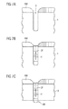
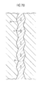
- FIGS. 7A to 7C show simplified partial sectional views to illustrate an alternative manufacturing step especially for filling the trenches with a shear stress resistant Material, the same reference numerals being the same or designate corresponding layers or elements as in Figures 1 to 6 and a repeated description is subsequently waived.
- a Oxide hard mask HM not only formed or etched the trenches G. be, but in a step according to Figure 7B Using the electroplating process described above and the hard mask HM as a protective layer also with a metallic material as shear-resistant material SF be replenished.
- Such electroplated metals SF are particularly resistant to this Shear stresses, which is why the spread of hairline cracks in particularly thin semiconductor wafers (i.e. less than 50 ⁇ m) can be prevented particularly reliably.
- cavities or so-called Voids V which with such a galvanic Deposition formed in the trenches or in the filling material SF avoid a layout can serve according to Figure 7D.
- V in the trenches can be avoided to avoid voids G the saw frame 4 the layout, for example in the form of a Jagged ZR are executed, which has the consequence that electroplating specifically before the metal grows together finished in the wider areas of the zigzag edge ZR then the proportion of Voids V is small compared to that Proportion of the trench thickness where the metal SF has grown together properly is.
- the Voids V with straight edges may be from purely random, microscopic fluctuations in the Trench width depends on it and therefore its extent cannot be controlled are.
- the thinned semiconductor wafer 1A again has a final thickness, which is smaller than the depth of the trench G, the structures protruding on the back as alignment marks JM used for a particularly easy front-back adjustment can be.
- shear-resistant material SF which is formed galvanically in the trench G can preferably Copper (Cu) can be used.
- Tungsten the metal with the most favorable properties, which is electroplated in the trenches G.
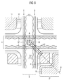
- Figure 8 shows a simplified partial top view of an ultra thin break-resistant semiconductor wafers according to a third exemplary embodiment, the same reference numerals being the same or designate corresponding elements or layers such as in Figures 1 to 7 and a repeated description is subsequently waived.
- a saw frame 4 has two from each other spaced trenches G, which with one of the above described methods are formed or filled can.
- Those separated from each other by the saw frame 4 Semiconductor components usually have a cell field ZF with active components, but also so-called connection surfaces GP, which is usually formed on insulating layers 8 are and therefore not at least not immediately can be galvanized.
- connection surfaces GP which is usually formed on insulating layers 8 are and therefore not at least not immediately can be galvanized.
- connection surfaces GP which is usually formed on insulating layers 8 are and therefore not at least not immediately can be galvanized.
- Conductor structures can preferably be used for this be that directly on the substrate surface or the surface of the
- Figure 9 shows a simplified partial sectional view along a section A-A according to Figure 8, with the same reference numerals same or corresponding layers as in Figures 1 to 8 and a repeated description below is waived.
- FIG. 9 is used to fill up the exposed, however area GP insulated by the insulating layer 8 for the gate connection areas an auxiliary structure HF on the surface of the semiconductor wafer 1 and at least on the surface of the Insulating layer 8 in the exposed insulated area GP to to a substrate area 19 in the saw frame 4, for example formed and structured via a trench G, whereby one a contact from the substrate area 19 to the isolated exposed area GP receives.
- the isolated exposed area is galvanically filled, which not only reduces shear stress material but also, for example, a so-called gate connection area or gate pad GP by means of those described above Electroplating process can be formed.
- the lines RS indicate the edges of the sawing track in the saw frame 4, whereby the gate connection areas GP from electrically conductive carrier substrate are separated.
- Figure 10 shows a simplified partial sectional view of a Cell field ZF according to a fourth embodiment, wherein same reference numerals same or corresponding layers or designate elements as in FIGS. 1 to 9 and a repeated description is omitted below becomes.
- local p-wells 9A are formed in an n - semiconductor substrate 1 as so-called p-bodies, into which source regions S are introduced on the surface.
- p-bodies On the surface of the semiconductor substrate 1 there is a gate insulation layer (not shown), a gate layer GS and an insulation layer 8, which are structured into cell stacks, in the usual way.
- Contact holes KL are also formed between each cell stack with a dimension L in the semiconductor substrate 1 or the p-wells 9A and through the source regions S, as a result of which the galvanization described above can be carried out.
- the galvanic filling layer 11A up to a line or a level N1, where you first of all receives separate plating plugs or mushrooms.
- these mushrooms 11A together, creating a galvanic Fill layer 11B, for example at a line or level N2 receives.
- the galvanization method according to the invention is in particular applicable when the cell grid L of the power transistors is much smaller than a height H of the galvanizing mask or bumps 6.
- the present invention by forming Trenches and filling these trenches with shear stress resistant Material disk-shaped objects and in particular semiconductor wafers made unbreakable. So these items or semiconductor wafers but still manageable after thinning remain, the disc-shaped objects or Semiconductor wafers through galvanization masks and in between lying galvanic filling layers further stabilized, whereby highly break-proof semiconductor wafers and associated semiconductor circuit arrangements receives.
- the invention has been described above using a silicon semiconductor wafer described. However, it is not limited to this and also includes other semiconductor materials in the same way. In the same way can be used as shear stress resistant Materials other than photoimide or Copper can be used to reduce similar properties or prevention of the shear stresses mentioned at the beginning exhibit.
Landscapes
- Chemical & Material Sciences (AREA)
- Engineering & Computer Science (AREA)
- Chemical Kinetics & Catalysis (AREA)
- Electrochemistry (AREA)
- Materials Engineering (AREA)
- Metallurgy (AREA)
- Organic Chemistry (AREA)
- Mechanical Treatment Of Semiconductor (AREA)
- Electroplating Methods And Accessories (AREA)
- Electrodes Of Semiconductors (AREA)
- Processing Of Stones Or Stones Resemblance Materials (AREA)
Abstract
Description
- Figur 1
- eine vereinfachte Seitenansicht eines herkömmlichen Halbleiterwafers bei der Ablage in einer Horde;
- Figur 2
- eine vereinfachte Seitenansicht eines ultradünnen Halbleiterwafers bei der Ablage in einer Horde;
- Figuren 3A bis 3D
- grafische Darstellungen zur Veranschaulichung einer Schnittkraft, einer Querkraft und einer Schubspannung für einen einseitig eingespannten Träger;
- Figur 4
- eine vereinfachte Teil-Draufsicht eines herkömmlichen Halbleiterwafers mit Haarriss;
- Figur 5
- eine vereinfachte perspektivische Teilansicht eines herkömmlichen Halbleiterwafers mit Haarriss;
- Figuren 6A bis 6C
- vereinfachte Teil-Schnittansichten zur Veranschaulichung wesentlicher Verfahrensschritte bei der Herstellung eines bruchfesten Halbleiterwafers gemäß einem ersten Ausführungsbeispiel;
- Figuren 7A bis 7D
- vereinfachte Teil-Schnittansichten sowie eine Teil-Draufsicht zur Veranschaulichung wesentlicher Verfahrensschritte beim Auffüllen der Gräben mit einem schubspannungsfesten Material gemäß einem zweiten Ausführungsbeispiel;
- Figur 8
- eine vereinfachte Teil-Draufsicht eines bruchfesten Halbleiterwafers gemäß einem dritten Ausführungsbeispiel;
- Figur 9
- eine vereinfachte Teil-Schnittansicht eines bruchfesten Halbleiterwafers entlang eines Schnitts A-A gemäß Figur 8; und
- Figur 10
- eine vereinfachte Teil-Schnittansicht eines Zellenfeldes des bruchfesten Halbleiterwafers gemäß einem vierten Ausführungsbeispiel.
Claims (24)
- Verfahren zur Herstellung eines bruchfesten scheibenförmigen Gegenstands mit den Schritten:a) Vorbereiten eines elektrisch leitenden Trägersubstrats (1) mit einer Anfangsdicke (DA) und einem Sägerahmen (4);b) Ausbilden von zumindest einem Graben (G1, G2) im Wesentlichen im Bereich des Sägerahmens (4) an einer Vorderseite des Trägersubstrats (1);c) Auffüllen des zumindest einen Grabens (G1, G2) mit einem schubspannungsfesten Material (SF);d) Ausbilden einer Galvanisierungsmaske (6) mit freiliegenden Bereichen an der Vorderseite des Trägersubstrats (1);e) Durchführen einer Galvanisierung des Trägersubstrates (1) zum Auffüllen der freiliegenden Bereiche der Galvanisierungsmaske (6); undf) Dünnen des Trägersubstrats (1) von seiner Rückseite bis zu einer Enddicke (DE1, DE2) zur Realisierung eines gedünnten Trägersubstrats (1A), wobei
in Schritt b) zumindest ein Graben (G1, G2) mit einer Grabentiefe (h1, h2) ausgebildet wird, die größer ist als die Enddicke (DE1, DE2) des gedünnten Trägersubstrats (1A). - Verfahren nach Patentanspruch 1,
dadurch gekennzeichnet, dass in Schritt a) ein Halbleiterwafer von einem ersten Leitungstyp (n-) verwendet wird. - Verfahren nach Patentanspruch 1 oder 2,
dadurch gekennzeichnet, dass in Schritt b) ein Laserschneiden, Plasmaätzen, nasschemisches Ätzen, lichtinduziertes Ätzen, anodisches Ätzen und/oder Sägen durchgeführt wird. - Verfahren nach einem der Patentansprüche 1 bis 3,
dadurch gekennzeichnet, dass
die Schritte c) und d) gleichzeitig durchgeführt werden. - Verfahren nach Patentanspruch 4,
dadurch gekennzeichnet, dass ein photosensitiver Lack als schubspannungsfestes Material (SF) ganzflächig aufgeschleudert sowie in den zumindest einen Graben (G1, G2) eingebracht, und zur Ausbildung der Galvanisierungsmaske (6) fotolithographisch strukturiert wird. - Verfahren nach Patentanspruch 5,
dadurch gekennzeichnet, dass der photosensitive Lack Fotoimid darstellt. - Verfahren nach einem der Patentansprüche 1 bis 3,
dadurch gekennzeichnet, dass
in Schritt c) ein metallisches Material und insbesondere Wolfram als schubspannungsfestes Material (SF) im zumindest einen Graben (G) galvanisch aufgefüllt wird. - Verfahren nach einem der Patentansprüche 1 bis 7,
dadurch gekennzeichnet, dass vor Schritt e) ein Schleifen zur Verringerung von Schwankungen der Anfangsdicke (DA) durchgeführt wird. - Verfahren nach einem der Patentansprüche 1 bis 8,
dadurch gekennzeichnet, dass in Schritt e) eine Vielzahl von galvanischen Metallschichten ausgebildet werden. - Verfahren nach einem der Patentansprüche 1 bis 9,
dadurch gekennzeichnet, dass in Schritt e) eine gleichförmige Kontaktierung des Trägersubstrats (1) von seiner Rückseite erfolgt. - Verfahren nach Patentanspruch 10,
dadurch gekennzeichnet, dass in Schritt e) ein Vakuumchuck mit einer Vielzahl von Kontaktspitzen (13) und dazwischenliegenden Vakuumkanälen (14) für die gleichförmige Kontaktierung verwendet wird. - Verfahren nach einem der Patentansprüche 1 bis 11,
dadurch gekennzeichnet, dass in Schritt f) ein mechanisches Schleifen mit nachfolgendem Spin-Ätzen und abschließendem Polieren durchgeführt wird. - Verfahren nach einem der Patentansprüche 1 bis 12,
dadurch gekennzeichnet, dass in Schritt f) bis zu einer Enddicke (DE1, DE2) von 5 µm bis 200 µm gedünnt wird. - Verfahren nach einem der Patentansprüche 1 bis 13,
dadurch gekennzeichnet, dass vor Schritt d) eine elektrisch leitende Hilfsstruktur (HS) zur Galvanisierung von isolierten freiliegenden Bereichen (GP) der Galvanisierungsmaske (6) ausgebildet wird, die mit einer Isolierschicht (8) bedeckt sind. - Verfahren nach Patentanspruch 14,
dadurch gekennzeichnet, dass die elektrisch leitende Hilfsstruktur (HS) eine von einem Substratbereich (19) im Sägerahmen (4) zu den isolierten freiliegenden Bereichen (GP) führende Leiterbahnstruktur darstellt. - Verfahren nach Patentanspruch 14 oder 15,
dadurch gekennzeichnet, dass die isolierten freiliegenden Bereiche Gate-Anschlussbereiche (GP) darstellen. - Halbleiterschaltungsanordnung mit
einem gedünnten Halbleitersubstrat (1A); und
zumindest einem Halbleiterbauelement (9; S, GS, D), welches im Halbleitersubstrat (1A) ausgebildet ist;
gekennzeichnet durch
zumindest einen Graben (G1, G2; G), der an einem Bausteinrand im Substrat (1A) ausgebildet und mit einem schubspannungsfesten Material (SF) aufgefüllt ist;
eine Galvanisierungsmaske (6), die an der Oberfläche des Halbleitersubstrats (1A) mit einer Vielzahl von freiliegenden Bereichen ausgebildet ist; und
einer galvanischen Füllschicht (11), welche die Vielzahl von freiliegenden Bereichen der Galvanisierungsmaske (6) im Wesentlichen gleichförmig auffüllt. - Halbleiterschaltungsanordnung nach Patentanspruch 17,
dadurch gekennzeichnet, dass die Galvanisierungsmaske (6) unmittelbar über dem zumindest einen Graben (G1, G2; G) ausgebildet ist und das gleiche Material aufweist wie das schubspannungsfeste Material (SF) des zumindest einen Grabens (G1, G2; G). - Halbleiterschaltungsanordnung nach Patentanspruch 18,
dadurch gekennzeichnet, dass das schubspannungsfeste Material (SF) des zumindest einen Grabens (G1, G2; G) und das Material der Galvanisierungsmaske (6) einen photosensitiven Lack und insbesondere Photoimid aufweist. - Halbleiterschaltungsanordnung nach Patentanspruch 17,
dadurch gekennzeichnet, dass das schubspannungsfeste Material (SF) des zumindest einen Grabens (G1, G2; G) eine galvanische Füllschicht und insbesondere Wolfram aufweist. - Halbleiterschaltungsanordnung nach einem der Patentansprüche 17 bis 20, gekennzeichnet durch eine elektrisch leitende Hilfsstruktur (HS), die an der Oberfläche des Halbleitersubstrats (1A) ausgebildet ist und von einem Bausteinrand zu isolierten freiliegenden Bereichen (GP) der Galvanisierungsmaske (6) führt, die mit einer Isolierschicht (8) bedeckt sind.
- Halbleiterschaltungsanordnung nach einem der Patentansprüche 17 bis 21, dadurch gekennzeichnet, dass das zumindest eine Halbleiterbauelement (9; S, GS, D) einen vertikalen Leistungstransistor darstellt.
- Halbleiterschaltungsanordnung nach Patentanspruch 22, dadurch gekennzeichnet, dass die isolierten freiliegenden Bereiche (GP) Gate-Anschlussbereiche für eine Gateschicht (GS) des Leistungstransistors darstellen.
- Halbleiterschaltungsanordnung nach einem der Patentansprüche 17 bis 23, dadurch gekennzeichnet, dass der zumindest eine Graben (G) einen Zackenrand (ZR) aufweist.
Applications Claiming Priority (2)
| Application Number | Priority Date | Filing Date | Title |
|---|---|---|---|
| DE10326507 | 2003-06-12 | ||
| DE10326507A DE10326507A1 (de) | 2003-06-12 | 2003-06-12 | Verfahren zur Herstellung eines bruchfesten scheibenförmigen Gegenstands sowie zugehörige Halbleiterschaltungsanordung |
Publications (2)
| Publication Number | Publication Date |
|---|---|
| EP1489656A2 true EP1489656A2 (de) | 2004-12-22 |
| EP1489656A3 EP1489656A3 (de) | 2006-03-08 |
Family
ID=33394818
Family Applications (1)
| Application Number | Title | Priority Date | Filing Date |
|---|---|---|---|
| EP04101941A Withdrawn EP1489656A3 (de) | 2003-06-12 | 2004-05-05 | Verfahren zur Herstellung eines bruchfesten scheibenförmigen Gegenstands sowie zugehörige Halbleiterschaltungsanordnung |
Country Status (2)
| Country | Link |
|---|---|
| EP (1) | EP1489656A3 (de) |
| DE (1) | DE10326507A1 (de) |
Cited By (2)
| Publication number | Priority date | Publication date | Assignee | Title |
|---|---|---|---|---|
| EP1505638A3 (de) * | 2003-06-12 | 2009-03-11 | Infineon Technologies AG | Verfahren zur Herstellung eines bruchfesten, scheibenförmigen Gegenstands sowie zugehörige Halbleiterschaltungsanordnung |
| CN111540706A (zh) * | 2020-04-22 | 2020-08-14 | 创能动力科技有限公司 | 用于制造具有支撑结构的半导体晶片的方法 |
Families Citing this family (1)
| Publication number | Priority date | Publication date | Assignee | Title |
|---|---|---|---|---|
| DE102007043902A1 (de) * | 2007-09-14 | 2009-03-19 | Osram Opto Semiconductors Gmbh | Verfahren zum Vereinzeln metallisierter Halbleiterbauelemente |
Family Cites Families (7)
| Publication number | Priority date | Publication date | Assignee | Title |
|---|---|---|---|---|
| US5104820A (en) * | 1989-07-07 | 1992-04-14 | Irvine Sensors Corporation | Method of fabricating electronic circuitry unit containing stacked IC layers having lead rerouting |
| CA2118994A1 (en) * | 1993-06-21 | 1994-12-22 | Claude L. Bertin | Polyimide-insulated cube package of stacked semiconductor device chips |
| US5618752A (en) * | 1995-06-05 | 1997-04-08 | Harris Corporation | Method of fabrication of surface mountable integrated circuits |
| US5691248A (en) * | 1995-07-26 | 1997-11-25 | International Business Machines Corporation | Methods for precise definition of integrated circuit chip edges |
| JP3537447B2 (ja) * | 1996-10-29 | 2004-06-14 | トル‐シ・テクノロジーズ・インコーポレイテッド | 集積回路及びその製造方法 |
| US6882030B2 (en) * | 1996-10-29 | 2005-04-19 | Tru-Si Technologies, Inc. | Integrated circuit structures with a conductor formed in a through hole in a semiconductor substrate and protruding from a surface of the substrate |
| US20030189215A1 (en) * | 2002-04-09 | 2003-10-09 | Jong-Lam Lee | Method of fabricating vertical structure leds |
-
2003
- 2003-06-12 DE DE10326507A patent/DE10326507A1/de not_active Ceased
-
2004
- 2004-05-05 EP EP04101941A patent/EP1489656A3/de not_active Withdrawn
Cited By (2)
| Publication number | Priority date | Publication date | Assignee | Title |
|---|---|---|---|---|
| EP1505638A3 (de) * | 2003-06-12 | 2009-03-11 | Infineon Technologies AG | Verfahren zur Herstellung eines bruchfesten, scheibenförmigen Gegenstands sowie zugehörige Halbleiterschaltungsanordnung |
| CN111540706A (zh) * | 2020-04-22 | 2020-08-14 | 创能动力科技有限公司 | 用于制造具有支撑结构的半导体晶片的方法 |
Also Published As
| Publication number | Publication date |
|---|---|
| DE10326507A1 (de) | 2005-01-13 |
| EP1489656A3 (de) | 2006-03-08 |
Similar Documents
| Publication | Publication Date | Title |
|---|---|---|
| DE10315780B4 (de) | Herstellungsverfahren für Halbleitervorrichtungen | |
| DE102013112797B4 (de) | Anordnung mit halbleitervorrichtung einschliesslich eines chipträgers, halbleiterwafer und verfahren zum herstellen einer halbleitervorrichtung | |
| WO2000074134A1 (de) | Verfahren zur vertikalen integration von elektrischen bauelementen mittels rückseitenkontaktierung | |
| EP0666595A1 (de) | Verfahren zur Herstellung einer kubisch integrierten Schaltungsanordnung | |
| DE102004052921A1 (de) | Verfahren zur Herstellung von Halbleiterbauelementen mit externen Kontaktierungen | |
| DE112013001641T5 (de) | Solarzelle und Verfahren zum Herstellen einer Solarzelle | |
| DE112021000892T5 (de) | Halbleiterbauteil, ein dieses aufweisendes halbleitergehäuse, und verfahren zur herstellung eines halbleiterbauteils | |
| DE102006052202B3 (de) | Halbleiterbauelement sowie Verfahren zur Herstellung eines Halbleiterbauelements | |
| DE1924712C3 (de) | Integrierter Dünnschicht-Abblockbzw. Entkopplungskondensator für monolithische Schaltungen und Verfahren zu seiner Herstellung | |
| DE102009044060A1 (de) | Solarzellenkontaktierungsverfahren, Solarzellenanordnung, Solarzellenstring und Solarzellenmodul | |
| DE102015110437A1 (de) | Halbleitervorrichtung mit einer Metallstruktur, die mit einer leitfähigen Struktur elektrisch verbunden ist | |
| DE10127950A1 (de) | Verfahren zur Herstellung eines Halbleiterbauelements und Halbleiterbauelement | |
| DE102006019950B4 (de) | Halbleitervorrichtung mit dielektrischer Trennung | |
| DE69321966T2 (de) | Leistungs-Halbleiterbauelement | |
| DE102009005458A1 (de) | Halbleiterbauelement mit Durchkontaktierung und Verfahren zu dessen Herstellung | |
| DE102008036285B4 (de) | Integrierte Schaltung mit einer durch einen galvanischen Prozess erzeugten Verbindung mit einem Kühlkörper und Verfahren dazu | |
| EP1489656A2 (de) | Verfahren zur Herstellung eines bruchfesten scheibenförmigen Gegenstands sowie zugehörige Halbleiterschaltungsanordnung | |
| DE102008033223A1 (de) | Kontaktstruktur mit selektivem Emitter | |
| WO2009156382A2 (de) | Verfahren zum herstellen einer thermoelektrischen vorrichtung | |
| DE102018112979A1 (de) | Monolithisch integrierter chip einschliesslich aktiver elektrischer komponenten und passiver elektrischer komponenten mit chipkantenstabilisierungsstrukturen | |
| DE102007002156A1 (de) | Halbleiteranordnung mit Wärmesenke | |
| DE102006043163B4 (de) | Halbleiterschaltungsanordnungen | |
| DE112012004917T5 (de) | Verfahren zum Verhindern eines elektrischen Kurzschlusses in einem Halbleiterschichtstapel, CPV-Zelle mit dünnem Substrat und Solarzellenanordnung | |
| DE102018103169A1 (de) | Verfahren zur Herstellung eines Halbleiterbauelements und Halbleiterbauelement | |
| DE4309898B4 (de) | Verfahren zur Herstellung eines Bipolartransistors mit einer Polysiliziumschicht zwischen einem Halbleiterbereich und einem Oberflächenelektrodenmetall |
Legal Events
| Date | Code | Title | Description |
|---|---|---|---|
| PUAI | Public reference made under article 153(3) epc to a published international application that has entered the european phase |
Free format text: ORIGINAL CODE: 0009012 |
|
| AK | Designated contracting states |
Kind code of ref document: A2 Designated state(s): AT BE BG CH CY CZ DE DK EE ES FI FR GB GR HU IE IT LI LU MC NL PL PT RO SE SI SK TR |
|
| AX | Request for extension of the european patent |
Extension state: AL HR LT LV MK |
|
| PUAL | Search report despatched |
Free format text: ORIGINAL CODE: 0009013 |
|
| AK | Designated contracting states |
Kind code of ref document: A3 Designated state(s): AT BE BG CH CY CZ DE DK EE ES FI FR GB GR HU IE IT LI LU MC NL PL PT RO SE SI SK TR |
|
| AX | Request for extension of the european patent |
Extension state: AL HR LT LV MK |
|
| 17P | Request for examination filed |
Effective date: 20060413 |
|
| AKX | Designation fees paid |
Designated state(s): DE |
|
| STAA | Information on the status of an ep patent application or granted ep patent |
Free format text: STATUS: THE APPLICATION IS DEEMED TO BE WITHDRAWN |
|
| 18D | Application deemed to be withdrawn |
Effective date: 20080201 |