EP1484946A2 - Organic electroluminescent display panel, method of manufacturing it and display device equiped with the panel - Google Patents
Organic electroluminescent display panel, method of manufacturing it and display device equiped with the panel Download PDFInfo
- Publication number
- EP1484946A2 EP1484946A2 EP04013252A EP04013252A EP1484946A2 EP 1484946 A2 EP1484946 A2 EP 1484946A2 EP 04013252 A EP04013252 A EP 04013252A EP 04013252 A EP04013252 A EP 04013252A EP 1484946 A2 EP1484946 A2 EP 1484946A2
- Authority
- EP
- European Patent Office
- Prior art keywords
- microlens
- electrode
- light
- panel
- microlenses
- Prior art date
- Legal status (The legal status is an assumption and is not a legal conclusion. Google has not performed a legal analysis and makes no representation as to the accuracy of the status listed.)
- Withdrawn
Links
Images


Classifications
-
- H—ELECTRICITY
- H05—ELECTRIC TECHNIQUES NOT OTHERWISE PROVIDED FOR
- H05B—ELECTRIC HEATING; ELECTRIC LIGHT SOURCES NOT OTHERWISE PROVIDED FOR; CIRCUIT ARRANGEMENTS FOR ELECTRIC LIGHT SOURCES, IN GENERAL
- H05B33/00—Electroluminescent light sources
- H05B33/10—Apparatus or processes specially adapted to the manufacture of electroluminescent light sources
-
- H—ELECTRICITY
- H10—SEMICONDUCTOR DEVICES; ELECTRIC SOLID-STATE DEVICES NOT OTHERWISE PROVIDED FOR
- H10K—ORGANIC ELECTRIC SOLID-STATE DEVICES
- H10K59/00—Integrated devices, or assemblies of multiple devices, comprising at least one organic light-emitting element covered by group H10K50/00
- H10K59/80—Constructional details
- H10K59/875—Arrangements for extracting light from the devices
- H10K59/879—Arrangements for extracting light from the devices comprising refractive means, e.g. lenses
-
- H—ELECTRICITY
- H10—SEMICONDUCTOR DEVICES; ELECTRIC SOLID-STATE DEVICES NOT OTHERWISE PROVIDED FOR
- H10K—ORGANIC ELECTRIC SOLID-STATE DEVICES
- H10K50/00—Organic light-emitting devices
- H10K50/80—Constructional details
- H10K50/85—Arrangements for extracting light from the devices
- H10K50/858—Arrangements for extracting light from the devices comprising refractive means, e.g. lenses
-
- H—ELECTRICITY
- H10—SEMICONDUCTOR DEVICES; ELECTRIC SOLID-STATE DEVICES NOT OTHERWISE PROVIDED FOR
- H10K—ORGANIC ELECTRIC SOLID-STATE DEVICES
- H10K59/00—Integrated devices, or assemblies of multiple devices, comprising at least one organic light-emitting element covered by group H10K50/00
- H10K59/10—OLED displays
- H10K59/12—Active-matrix OLED [AMOLED] displays
Definitions
- the present invention relates to an organic electroluminescent display device and a method of manufacturing it, the organic electroluminescent display device making a display through the light-emitting state of a plurality of organic luminescent layers.
- CRTs Cathode Ray Tubes
- flat display panels composed of various types of elements.
- Flat display panels are light-weight and have a better luminous efficiency than CRTs, and have been developed over the years for use as monitor screens for computers and televisions and the like.
- active matrix driven organic EL Electrode Electrode
- an organic EL display a thin film including a fluorescent inorganic and organic compound is sandwiched between a cathode and an anode; an array of elements of such structure are provided that are selectively induced to emit light using the radiation of light (fluorescence, phosphorescence) produced when excitons decay that have been generated by recombination of electrons and holes injected into the thin film.
- Such active matrix driven organic EL displays are getting a lot of attention as they feature a thin structure and high resolution.
- FIG. 10 is a sectional view showing an example of a configuration of an organic EL panel 101a included in a conventional organic EL display.
- the organic EL panel 101a has a light-emitting element 114 and a desiccant 109 sealed through a transparent glass 111 and a sealing glass 111 a.
- the space sealed by the glass 111 and the sealing glass 111a is desiccated by the desiccant 109, and light Lp emitted by a light-emitting element 114 crosses the glass 111 and is emitted to the outside.
- JP 10-172756 A discloses an organic EL light-emitting device designed to solve such problems.
- This known organic EL light-emitting device has a microlens 2 located inside a light transmissive base board 1 as shown in FIG. 1 of the document, a microlens 22 located inside a light transmissive base board 21 as shown in FIG. 2 of the document, and microlenses 32 and 33 located inside a light transmissive base board 31 as shown in FIG. 3 of the document.
- a conventional configuration it is difficult and thus costly to place the microlens 2 inside the light transmissive base board 1. Further, in its FIG.
- this document JP 10-172756 A shows a configuration wherein a microlens 42 is provided inside a backing layer 43 that is formed on a light transmissive base board 41.
- the microlens inside the backing layer 43 has a convexly curved surface form on the side of the light transmissive base board 41 rather than on the side of the lower electrode 44a.
- the difficulty with manufacturing is seemingly resolved because the microlens 42 is not formed inside the light transmissive base board 41 anymore.
- JP 10-172756 A no concrete manufacturing procedure is disclosed regarding the organic EL light-emitting device 40 shown in FIG. 4 thereof. Further, for the active matrix driven organic EL light-emitting device 40, the manufacture itself seems problematical, as the substrate process becomes a high temperature process of about 500 °C that requires the microlens 42 itself to be able to withstand such high temperatures.
- the present invention is intended to solve the above-mentioned problems and its object is to provide a method of manufacturing an organic electroluminescent display device, an organic electroluminescent display panel, and a display device equipped with the panel that enable to form a microlens without affecting an organic luminescent layer during the manufacturing process, and to easily manufacture an organic electroluminescent display device with increased light output efficiency.
- a microlens can be easily formed by performing photolithography and reflow treatment on a transparent resin before the organic luminescent layer is formed. Therefore, an adverse affect on the heat-sensitive organic luminescent layer when forming the microlens can be avoided.
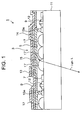
- FIG. 1 is a sectional view of one embodiment of an organic electroluminescent panel 1 (simply referred to as "EL panel” hereinafter) according to the present invention.
- the EL panel 1 is to be mounted in a display device, and includes a substrate 11, arrays of microlenses 17, a low refractive index resin 5, transistors 12, a wiring 7, insulating layers 9, and a plurality of (organic) EL elements each comprising an anode 15, an organic luminescent layer 14 (referred to as "OL layer hereinafter), and a cathode 13.
- This EL panel 1 is a sealant substrate light-emitting organic EL panel that emits light from the surface of the substrate 11 towards the outside (lower part of the drawing).
- the substrate 11 is a transparent substrate like a glass plate. On this substrate, a layer of the resin 5 is provided. Inside this resin 5, arrays of microlenses 17 are formed. Also within this resin 5, the transistors 12, the wiring 7 and opening parts 15a that extend from the anodes 15 are provided.
- the microlenses 17 are composed of a transparent resin with a high refractive index, for example a refractive index (nD) from 1.5 to 1.8. On the other side, the resin 5 has a low refractive index, for example a refractive index (nD) from 1.2 to less than 1.5.
- the refractive index (nD) of the microlenses 17 is 1.5 or more, because the larger the difference between the refractive index of the resin 5 and that of the microlenses 17, the stronger the power of the microlenses, and thereby all of the scattered light (light arriving at the microlens 17 from various directions) is sufficiently refracted to exceed the critical angle, i.e., is refracted by the microlens to reach the interface between the microlens 17 and the substrate 11 at an angle larger then the critical angle, and the EL panel 1 can have a minimum of loss of light. If it is less than 1.5, there is a risk of a total reflection phenomenon occurring at the interface with the substrate 11 having a refractive index (nD) of for example 1.5.
- the refractive index of the microlenses 17 it is preferable for the refractive index of the microlenses 17 to be 1.8 or less, because a refractive index of the microlenses 17 exceeding 1.8 leads to a combination where the difference in refractive index between the microlenses and the resin 5 exceeds 0.6. In that combination there is a risk that the reflection at the interface gets too large and the light output efficiency thus decreases.
- the refractive index of the resin 5 it is preferable for the refractive index of the resin 5 to be 1.2 or more, as it otherwise leads to a combination where the difference in refractive index between the resin 5 and the microlenses 17 exceeds 0.6 with the result just mentioned. Further, it is preferable for the refractive index of the resin 5 to be less than 1.5, as it otherwise leads to a combination where the difference in refractive index between the resin 5 and the microlenses 17 falls below 0.1. In that combination the power of the microlenses is weak, and not all of the scattered can be refracted to exceed the critical angle, leading to an EL panel 1 with a large loss of light.
- the diameter of the microlenses 17 is preferably from 1 ⁇ m to 50 ⁇ m. It is preferable for this diameter to be 1 ⁇ m or more, as otherwise, due to a diffraction phenomenon of the light, the focal power of the microlenses decreases and becomes too small. Further, it is preferable for the diameter of the microlenses 17 to be 50 ⁇ m or less, because when the diameter exceeds 50 ⁇ m, the distance between a light-emitting part and the corresponding microlens 17 is too close compared with the focal distance of the microlens, and therefore not all of the scattered light can be refracted to exceed the critical angle, leading to an increase in negative influences such as an increased loss of light.
- the EL panel 1 can be achieved with a minimum of loss of light by choosing the optimum diameter of the microlenses 17 to be 1 ⁇ m to 50 ⁇ m.
- the cathodes 13, the OL layers 14 and the anodes 15 are provided on the resin 5, the cathodes 13, the OL layers 14 and the anodes 15 are provided.
- the cathodes and the anodes are provided to intersect each other so as to define a matrix structure.
- the cathode 13, the organic luminescent layer 14 and the anode 15 at each intersection of a cathode and an anode compose an (organic) EL element.
- Plural such EL elements are provided on the low refractive index resin 5, each representing a pixel 3.
- the transistors 12 are provided as switching elements that are controlled by the intersecting cathodes 13 and anodes 15.
- Each transistor 12 has the function to control the light-emitting state of the respective organic luminescent layer 14 that is provided between the corresponding cathode 13 and anode 15. That is to say, this transistor 12 has the function to actively drive the EL element that includes the respective organic luminescent layer 14. Further, to insulate the OL layers 14 from one another on the resin 5 the insulating layers 9 are provided.
- Each OL layer 14 is associated with at least one microlens 17.
- a microlens array of more than one microlens 17 is provided for each OL layer 14 (each EL element). With such a configuration, due to the existence of more than one microlens 17, the efficiency of the light output and the luminance of the light from each OL layer 14 improves.
- the pitch of the microlenses 17 in these microlens arrays is preferably within a range of for example 1 to 100 ⁇ m.
- each pixel 3 can be associated with a microlens array (MLA) composed of more than one microlens 17, and thus the height of the microlens 17 can be kept low.
- MLA microlens array
- the gap between the OL layer 14 and the microlens array can be filled in the EL panel 1, a high contrast picture can be achieved with no crosstalk between pixels 3 that could be caused when the light emitted from each pixel 3 is mixed and then condensed by the microlens 17.
- Characteristic in the present embodiment is, that the microlenses 17 are provided between the anode 15 and the substrate 11. Furthermore characteristic in the present embodiment is, that as mentioned above, the microlenses 17 have on the side of the anode 15 a convexly curved surface form. With such a configuration, it becomes less likely for the light generated in the OL layer 14 to exceed the critical angle at which the light will be reflected without crossing (passing through) the microlens 17 in the case of crossing the convex surface of the microlens 17 on the side of the anode 15 as compared to the case of crossing the convex surface of the microlens 17 on the side of the substrate 11. Therefore, forming the convex surface of the microlens 17 on the side of the anode 15 will lead to an increased output efficiency of light generated by the OL layer 14 and the EL panel 1 with reduced electrical power consumption can be composed.
- the EL panel 1 being of the above configuration, an explanation follows of an example of the behavior of the EL panel 1.
- each EL element is driven by the active matrix drive.
- the cathodes 13 and the anodes 15 compose a matrix structure, and by applying a voltage between a particular cathode 13 and a particular anode 15 the pixel 3 at the intersection between them is selected, i.e., the transistor 12 corresponding to this pixel is controlled, and due to the operation of that transistor 12, a current will flow in the OL layer 14 that is provided between the cathode 13 and the anode 15, thus inducing the OL layer 14 to emit light.
- the light generated by the OL layer 14 crosses the anode 15 that is transparent and the resin 5 that has a low refractive index, and enters the microlens 17.
- the microlens 17 has a higher refractive index than the resin 5, the light generated by the OL layer 14 is refracted, crosses the substrate 11 and is emitted to the outside part of the EL panel 1.
- the microlens 17 has a convex surface on the side of the anode 15, the light from the OL layer 14 can cross the substrate 11 efficiently without being affected by the critical angle at the boundary between the microlens 17 and the substrate 11.
- FIGs. 2 to 7 are sectional views illustrating individual steps of one embodiment of the manufacturing method of the EL panel 1 shown in FIG. 1.
- a transparent substrate 11 of a non-alkali glass material for example is prepared.
- wirings 7 constituting the circuit transistors 12 being for example polycrystalline silicon thin film transistors, condensers and the like are formed.
- a film is formed of a resin (photosensitive high refractive index resin 17a) as a base material for forming the microlenses 17.
- a resin photosensitive high refractive index resin 17a
- MFR-344H made by JRS with a refractive index (nD) of 1.62
- nD refractive index
- a method of forming the film of the resin 17a for example spin coating is used.
- the film of resin 17a is formed by spin coating with a film thickness of 3.0 ⁇ m for example.
- Lens patterns smaller than a pixel 3 are formed of about 33 ⁇ m square by applying photolithography technology against the resin 17a formed in such a way.
- the substrate 11 onto which lens patterns as shown in FIG. 2b have been formed is then processed by reflow treatment by putting it into a clean oven at 180 °C for 30 minutes for example, and a lens form as shown in FIG. 3a is formed corresponding to the form of the microlenses 17 that refracts the light from the OL layer 14.
- an acrylic resin with a refractive index of about 1.38 is applied by spin coating or the like onto the surface of the substrate 11 on which, among others, the microlenses 17 are formed, and by putting it into a clean oven with an atmosphere of about 180 °C for about 30 minutes the surface of this acrylic resin is caused to reflow, and planarization is carried out resulting in the layer of resin 5 shown in FIG. 3b.
- the planarized resin 5 is composed so as to cover the microlenses 17 and the other elements formed on the substrate 11.
- a resist (not shown) is coated, and by dry etching using oxygen for example, the opening parts 15a are formed at desired positions as shown in FIG. 4a.
- a film of about 100 nm including for example mainly indium tin oxide (ITO) is formed by sputtering as shown in FIG. 4b, and, patterning of the film to obtain the anodes 15 of the pixels 3 is carried out by a photolithographic technology.
- ITO indium tin oxide
- the insulating layers 9 are formed.
- the division of the pixels 3 becomes definite.
- an OL layer 14 is formed on each anode 15 by evaporation for example.
- the cathodes 13 are formed on the OL layers 14 and the insulating layers 9.
- defined sealing is carried out, and as shown in FIG. 1, the active matrix driven EL panel 1 having the microlenses 17 is completed.
- the microlenses 17 can be easily formed by performing photolithographic treatment and reflow treatment on the photosensitive high refractive index resin 17a, as shown in FIG. 2b, before forming the OL layers 14.
- the OL layers 14 being sensitive to heat are negatively affected when the microlenses 17 are formed. Further, not only can the luminance efficiency be increased for the EL panel 1 having the microlens arrays, but providing microlenses 17 having a convex surface on the side of the anode 15 results in an increase of the margin of the critical angle at which the light from the OL layer 14 is reflected by the microlens 17, and thus, the output efficiency of light can be further improved. Therefore, at a luminance that is the same as that of conventional organic EL panels, with a lower power consumption than conventionally, the luminous lifetime can be lengthened. Consequently, an advantage such as the above-mentioned one can be also obtained for a display device equipped with the EL panel 1.
- planarization is carried out by causing reflow at a given temperature, after applying an acrylic resin by spin coating as a base material for the resin 5. Planarization, though, may also be carried out by a method such as the one described in the following.
- an acrylic resin with a refractive index of 1.38 for example is applied as the resin 5.
- an acrylic resin World Rock No. 7702 produced by Kyoritsu Chemical can be used for example.
- the acrylic resin applied onto the substrate 11, as shown in FIG. 7, then undergoes an adhesion and hardening process to hold a quartz substrate (glass substrate) 4 of a thickness of for example 3 mm.
- a water repellency treatment on the surface of the quartz substrate 4 before it is brought into contact with the resin 5.
- a silane coupling agent or the like such as HMDS (hexamethyldisilazane) are adequate.
- plasma deposition by CF gas can be given as an example.
- the quartz substrate 4 is taken off, and as shown in FIG. 3b, the surface of the resin 5 undergoes planarization.
- the adhesion force of the resin 5 being originally adhesive for example is almost reduced to zero, and the quartz substrate 4 can be removed easily.
- the surface of the resin 5 from which the quartz substrate 4 has been removed can be made to be smooth.
- the opening parts 15a are formed as described before.
- the present invention is not limited to the above-described embodiment, and various modifications can be made within the scope of the Claims.
- part of them can be omitted and arbitrarily combined to differ from the above.
- a silicon oxide film of for example 60 nm may be inserted between the resin 5 and the anodes 15. With such a configuration, the adhesion can be improved between the resin 5 and the anodes 15.
- the EL panel 1 is explained as using a low-molecular organic luminescent layer for the EL element for example, but, as shown in FIG. 8, a macro-molecule organic layer EL element can also be used to obtain the same effect.
- the high-molecular organic EL material can be selectively applied as a liquid by using an inkjet process. Therefore, if a wall called bank is formed on the panel between pixels to separate each pixel from the others, so that the liquid does not flow to the other pixels, a panel can be manufactured just as the low-molecular organic EL.
- the above embodiment is not limited to a configuration of an EL panel 1a as shown in FIG. 8, but can also be applied to an EL panel 1b with color filter shown in FIG. 9.
- this EL panel 1 b practically the same processes as the above-mentioned processes can be used, and in addition to the configuration of the EL panel 1a shown in FIG. 8, color filter layers 2B, 2R, 2G are formed by a color filter resist between the resin 5 and the anodes 15. With such a configuration, a full color display device can be achieved that uses an organic EL panel emitting white light.
Landscapes
- Physics & Mathematics (AREA)
- Optics & Photonics (AREA)
- Engineering & Computer Science (AREA)
- Manufacturing & Machinery (AREA)
- Electroluminescent Light Sources (AREA)
Abstract
Description
- FIG. 1
- is a sectional view showing an example of a configuration of an organic EL panel in accordance with an embodiment of the invention;
- FIGS. 2
- to 6 are sectional views illustrating steps of an example of a manufacturing method of the organic EL panel;
- FIG. 7
- is a sectional view illustrating an alternative method step;
- FIG. 8
- is a sectional view showing an example of an application of the organic EL panel in accordance with the present embodiment;
- FIG. 9
- is a sectional view showing an example of an application of the organic EL panel in accordance with the present embodiment;
- FIG. 10
- is a sectional view showing an example of a conventional configuration of an organic EL panel.
Claims (8)
- A method of manufacturing an organic electroluminescent display panel having surface emitting elements, comprising:wherein each switching element (12) is connected to one of said first and one of said second electrodes (13) so as to be controlled by the respective first electrode (15) second electrode (13) and to control the light-emitting state of the organic luminescent layer (14) provided between that respective first electrode (15) and second electrode (13).a) forming, on a transparent substrate (11), a plurality of switching elements (12);b) forming a lens pattern (17a) of microlenses (17) by applying a first transparent resin onto the substrate (11) and subjecting it to a photolithographic treatment, followed by a reflow treatment on the lens pattern (17a) so as to form the microlenses (17);c) applying a second transparent resin (5) having a lower refractive index than the first transparent resin so as to cover the microlenses (17), and then hardening the second transparent resin (5);d) forming transparent first electrodes (15) on the second transparent resin (5);e) forming a respective organic luminescent layer (14) on each first electrode (15); andf) forming second electrodes (13) on the organic luminescent layers (14), the second electrodes (13) being formed so as to intersect with the first electrodes (15) to define a matrix structure;
- The method according to Claim 1, wherein step c) comprises applying the second transparent resin (5) and then hardening it while pressing a flat plate (4) against it.
- The method according to Claim 1 or 2, wherein step b) comprises applying a film of the second transparent resin (5) onto the substrate (11) by spin coating.
- The method according to any one of Claims 1 through 3, wherein step b) comprises forming the microlenses (17) so as to have a convexly curved surface on the side facing the first electrode (15).
- An organic electroluminescent display panel, comprising:a transparent substrate (11);switching elements (12) controlled by transparent first electrodes (15) and second electrodes (13) that are arranged to intersect each other so as to define a matrix form;surface emitting elements each having an organic luminescent layer (14) whose light-emitting state is controlled by a respective switching element (12), the organic luminescent layer (14) being provided between the first electrode (15) and the second electrode (13) controlling the respective switching element (12); anda microlens (17) provided between the substrate (11) and each first electrode (15) and having a convexly curved surface on the side facing the first electrode (15).
- The display panel according to Claim 5, wherein the diameter of the microlens (17) is from 1 µm to 50 µm.
- The display panel according to Claim 5 or 6, wherein a transparent resin (5) is provided between the microlens (17) and the first electrode (15), the refractive index of the microlens (17) being from 1.5 to 1.8, and the refractive index of the transparent resin (5) being from 1.2 to less than 1.5.
- The display panel according to any one of Claims 5 to 7, wherein for each organic luminescent layer (14) a plurality of corresponding microlenses (17) is provided.
Applications Claiming Priority (2)
| Application Number | Priority Date | Filing Date | Title |
|---|---|---|---|
| JP2003162687A JP2004363049A (en) | 2003-06-06 | 2003-06-06 | Method for manufacturing organic electroluminescence display device, organic electroluminescence display device, and display device including organic electroluminescence display device |
| JP2003162687 | 2003-06-06 |
Publications (2)
| Publication Number | Publication Date |
|---|---|
| EP1484946A2 true EP1484946A2 (en) | 2004-12-08 |
| EP1484946A3 EP1484946A3 (en) | 2007-03-21 |
Family
ID=33157226
Family Applications (1)
| Application Number | Title | Priority Date | Filing Date |
|---|---|---|---|
| EP04013252A Withdrawn EP1484946A3 (en) | 2003-06-06 | 2004-06-04 | Organic electroluminescent display panel, method of manufacturing it and display device equiped with the panel |
Country Status (6)
| Country | Link |
|---|---|
| US (2) | US7144752B2 (en) |
| EP (1) | EP1484946A3 (en) |
| JP (1) | JP2004363049A (en) |
| KR (1) | KR20040108606A (en) |
| CN (1) | CN100454568C (en) |
| TW (1) | TWI259026B (en) |
Cited By (3)
| Publication number | Priority date | Publication date | Assignee | Title |
|---|---|---|---|---|
| CN1929706B (en) * | 2005-09-05 | 2011-06-15 | 精工爱普生株式会社 | Organic electroluminescent device, method of manufacturing organic electroluminescent device, and electronic apparatus |
| WO2015059200A1 (en) * | 2013-10-24 | 2015-04-30 | Osram Oled Gmbh | Organic light-emitting diode and method for producing an organic light-emitting diode |
| US11769773B2 (en) | 2017-01-20 | 2023-09-26 | Sony Semiconductor Solutions Corporation | Display device, electronic device, and method of manufacturing display device with substrate including light emitting elements adhered to substrate including microlens array |
Families Citing this family (40)
| Publication number | Priority date | Publication date | Assignee | Title |
|---|---|---|---|---|
| JP4660143B2 (en) * | 2004-08-27 | 2011-03-30 | 富士フイルム株式会社 | Organic electroluminescent device and manufacturing method thereof |
| JP5153058B2 (en) * | 2005-02-25 | 2013-02-27 | 株式会社半導体エネルギー研究所 | Method for manufacturing semiconductor device |
| KR100912802B1 (en) | 2005-02-28 | 2009-08-18 | 삼성모바일디스플레이주식회사 | Electroluminescent display device |
| JP4747626B2 (en) * | 2005-03-25 | 2011-08-17 | セイコーエプソン株式会社 | Light emitting device |
| EP1875520A1 (en) * | 2005-04-13 | 2008-01-09 | Philips Intellectual Property & Standards GmbH | Structured substrate for a led |
| KR100703158B1 (en) * | 2005-10-24 | 2007-04-06 | 삼성전자주식회사 | Display device and manufacturing method |
| KR100717269B1 (en) | 2005-11-01 | 2007-05-15 | 삼성전자주식회사 | Display device and manufacturing method thereof |
| CN1967899B (en) * | 2005-11-15 | 2011-02-02 | 统宝光电股份有限公司 | Organic electroluminescence display element and manufacturing method thereof |
| JP2007207656A (en) * | 2006-02-03 | 2007-08-16 | Dainippon Printing Co Ltd | Organic EL display |
| JP5578846B2 (en) * | 2006-06-14 | 2014-08-27 | コーニンクレッカ フィリップス エヌ ヴェ | Structured OLED with micro-optical elements that generate directed light |
| TWI289815B (en) * | 2006-10-30 | 2007-11-11 | Au Optronics Corp | Electroluminescent display |
| CN100456527C (en) * | 2006-11-15 | 2009-01-28 | 吉林大学 | A method for improving the light-coupling efficiency of flat-panel light-emitting devices |
| KR20080069076A (en) * | 2007-01-22 | 2008-07-25 | 삼성전자주식회사 | Organic light emitting display |
| JP2009049135A (en) * | 2007-08-17 | 2009-03-05 | Sony Corp | Display device |
| KR20090061310A (en) * | 2007-12-11 | 2009-06-16 | 주식회사 동부하이텍 | Image sensor and its manufacturing method |
| JP2009272068A (en) * | 2008-04-30 | 2009-11-19 | Toppan Printing Co Ltd | El element, backlight apparatus for liquid crystal display using el element, lighting device using el element, electronic signboard device using el element, and display device using el element |
| US9722209B2 (en) | 2008-09-25 | 2017-08-01 | Lg Display, Co., Ltd. | Organic light-emitting diodes (OLEDS) with high efficiency and its manufacturing method |
| WO2011053004A2 (en) * | 2009-10-29 | 2011-05-05 | 주식회사 엘지화학 | Substrate having low reflection and high contact angle, and production method for same |
| JP2013008663A (en) * | 2011-05-24 | 2013-01-10 | Canon Inc | Display device |
| KR102028025B1 (en) * | 2012-11-13 | 2019-10-04 | 삼성디스플레이 주식회사 | Organic light emitting display apparatus and method of manufacturing the same |
| CN104730711A (en) * | 2013-12-20 | 2015-06-24 | 昆山国显光电有限公司 | Multimedia glasses and manufacturing method thereof |
| US9978814B2 (en) | 2015-10-30 | 2018-05-22 | Lg Display Co., Ltd. | Organic light emitting display device |
| KR101749147B1 (en) * | 2015-10-30 | 2017-06-21 | 엘지디스플레이 주식회사 | Organic light emitting display device and method for manufacturing the same |
| KR102737441B1 (en) * | 2015-10-30 | 2024-12-04 | 엘지디스플레이 주식회사 | Organic Light Emitting Diode Display Device |
| KR101739771B1 (en) | 2015-11-30 | 2017-05-26 | 엘지디스플레이 주식회사 | Organic light emitting display device and method for manufacturing the same |
| US10930709B2 (en) | 2017-10-03 | 2021-02-23 | Lockheed Martin Corporation | Stacked transparent pixel structures for image sensors |
| CN107706227B (en) * | 2017-10-26 | 2020-02-18 | 京东方科技集团股份有限公司 | A display substrate, its preparation method, and display device |
| KR102459045B1 (en) | 2017-11-30 | 2022-10-25 | 엘지디스플레이 주식회사 | Electroluminescent Display Device |
| US11616941B2 (en) | 2018-02-07 | 2023-03-28 | Lockheed Martin Corporation | Direct camera-to-display system |
| US10652529B2 (en) | 2018-02-07 | 2020-05-12 | Lockheed Martin Corporation | In-layer Signal processing |
| US10838250B2 (en) * | 2018-02-07 | 2020-11-17 | Lockheed Martin Corporation | Display assemblies with electronically emulated transparency |
| US10951883B2 (en) | 2018-02-07 | 2021-03-16 | Lockheed Martin Corporation | Distributed multi-screen array for high density display |
| JP7552588B2 (en) * | 2019-04-26 | 2024-09-18 | ソニーグループ株式会社 | Display devices and electronic devices |
| US11588137B2 (en) * | 2019-06-05 | 2023-02-21 | Semiconductor Energy Laboratory Co., Ltd. | Functional panel, display device, input/output device, and data processing device |
| KR20220031679A (en) | 2019-07-12 | 2022-03-11 | 가부시키가이샤 한도오따이 에네루기 켄큐쇼 | Function panel, display device, input/output device, information processing device |
| JPWO2021069999A1 (en) | 2019-10-11 | 2021-04-15 | ||
| US20210234132A1 (en) * | 2020-01-29 | 2021-07-29 | Sharp Kabushiki Kaisha | Shaped Filler Material In a QLED/OLED Pixel |
| JP7525512B2 (en) * | 2020-03-27 | 2024-07-30 | 京東方科技集團股▲ふん▼有限公司 | Display substrate and its manufacturing method, display device |
| CN113241354B (en) * | 2021-04-07 | 2022-07-12 | 武汉华星光电技术有限公司 | OLED display panel and preparation method thereof |
| CN114284455B (en) * | 2021-12-27 | 2024-11-26 | 视涯科技股份有限公司 | A display device |
Family Cites Families (19)
| Publication number | Priority date | Publication date | Assignee | Title |
|---|---|---|---|---|
| JPS61153602A (en) * | 1984-12-27 | 1986-07-12 | Matsushita Electronics Corp | Manufacture of microlens |
| US5561538A (en) * | 1992-11-17 | 1996-10-01 | Sharp Kabushiki Kaisha | Direct-view display apparatus |
| JP2730510B2 (en) * | 1995-02-22 | 1998-03-25 | 日本電気株式会社 | Drive circuit integrated type fluorescent display tube optical head |
| JPH0990337A (en) * | 1995-09-28 | 1997-04-04 | Sharp Corp | Transmissive liquid crystal display device |
| TW413993B (en) * | 1996-03-15 | 2000-12-01 | Sharp Kk | Image display device |
| US5948281A (en) * | 1996-08-30 | 1999-09-07 | Sony Corporation | Microlens array and method of forming same and solid-state image pickup device and method of manufacturing same |
| JP4073510B2 (en) * | 1996-12-13 | 2008-04-09 | 出光興産株式会社 | Organic EL light emitting device |
| JPH11354271A (en) * | 1998-06-05 | 1999-12-24 | Canon Inc | Photosensitive material writing device |
| CN1384970A (en) * | 1999-10-29 | 2002-12-11 | 普林斯顿大学理事会 | Organic Light Emitting Diodes with Spherical Patterns |
| JP2002182008A (en) * | 2000-10-04 | 2002-06-26 | Sharp Corp | Optical lens system, image display device, microlens array, liquid crystal display element, and projection type liquid crystal display device |
| JP4053260B2 (en) * | 2000-10-18 | 2008-02-27 | シャープ株式会社 | Organic electroluminescence display element |
| JP4717200B2 (en) | 2000-12-15 | 2011-07-06 | キヤノン株式会社 | Organic light emitting device |
| US7012363B2 (en) * | 2002-01-10 | 2006-03-14 | Universal Display Corporation | OLEDs having increased external electroluminescence quantum efficiencies |
| US6833667B2 (en) * | 2002-02-27 | 2004-12-21 | Matsushita Electric Industrial Co., Ltd. | Organic electroluminescence element and image forming apparatus or portable terminal unit using thereof |
| JP4126531B2 (en) | 2002-04-01 | 2008-07-30 | セイコーエプソン株式会社 | Image forming apparatus using organic EL array exposure head |
| DE60318145T2 (en) * | 2002-03-11 | 2008-12-24 | Seiko Epson Corp. | Optical writing head such as organic electroluminescent exposure head matrices, process for its production and image forming apparatus using the same |
| JP4183427B2 (en) | 2002-03-11 | 2008-11-19 | 三洋電機株式会社 | Electroluminescence element |
| US7511419B2 (en) * | 2002-05-14 | 2009-03-31 | Casio Computer Co., Ltd. | Luminescent panel having a reflecting film to reflect light outwardly which is shaped to condense the reflected light |
| JP4232541B2 (en) * | 2003-06-04 | 2009-03-04 | セイコーエプソン株式会社 | Manufacturing method of microlens device |
-
2003
- 2003-06-06 JP JP2003162687A patent/JP2004363049A/en active Pending
-
2004
- 2004-06-02 CN CNB200410049220XA patent/CN100454568C/en not_active Expired - Fee Related
- 2004-06-04 US US10/862,189 patent/US7144752B2/en not_active Expired - Fee Related
- 2004-06-04 EP EP04013252A patent/EP1484946A3/en not_active Withdrawn
- 2004-06-04 TW TW093116168A patent/TWI259026B/en not_active IP Right Cessation
- 2004-06-04 KR KR1020040040635A patent/KR20040108606A/en not_active Ceased
-
2006
- 2006-08-14 US US11/464,317 patent/US20060284554A1/en not_active Abandoned
Cited By (4)
| Publication number | Priority date | Publication date | Assignee | Title |
|---|---|---|---|---|
| CN1929706B (en) * | 2005-09-05 | 2011-06-15 | 精工爱普生株式会社 | Organic electroluminescent device, method of manufacturing organic electroluminescent device, and electronic apparatus |
| WO2015059200A1 (en) * | 2013-10-24 | 2015-04-30 | Osram Oled Gmbh | Organic light-emitting diode and method for producing an organic light-emitting diode |
| DE102013111736B4 (en) | 2013-10-24 | 2024-11-07 | Pictiva Displays International Limited | Organic light-emitting diode and method for producing an organic light-emitting diode |
| US11769773B2 (en) | 2017-01-20 | 2023-09-26 | Sony Semiconductor Solutions Corporation | Display device, electronic device, and method of manufacturing display device with substrate including light emitting elements adhered to substrate including microlens array |
Also Published As
| Publication number | Publication date |
|---|---|
| KR20040108606A (en) | 2004-12-24 |
| JP2004363049A (en) | 2004-12-24 |
| TW200511893A (en) | 2005-03-16 |
| CN1575056A (en) | 2005-02-02 |
| EP1484946A3 (en) | 2007-03-21 |
| US20050106776A1 (en) | 2005-05-19 |
| CN100454568C (en) | 2009-01-21 |
| US7144752B2 (en) | 2006-12-05 |
| US20060284554A1 (en) | 2006-12-21 |
| TWI259026B (en) | 2006-07-21 |
Similar Documents
| Publication | Publication Date | Title |
|---|---|---|
| EP1484946A2 (en) | Organic electroluminescent display panel, method of manufacturing it and display device equiped with the panel | |
| CN100355084C (en) | Double-plate type organic electroluminescent display device and manufacturing method | |
| US6806504B2 (en) | Active matrix organic electroluminescent display device and method of fabricating the same | |
| US7531834B2 (en) | Organic electroluminescent display device with improved interface between anode and luminescent organic layer | |
| US7663314B2 (en) | Organic electroluminescence display panel and method for sealing the same | |
| KR101281748B1 (en) | Top emission type organic electro-luminescence device | |
| KR101603145B1 (en) | Method of fabricating for dual panel type organic electro-luminescent device | |
| US8519616B2 (en) | Organic electroluminescent display device and method of fabricating the same | |
| CN1282064A (en) | Electroluminescence display device and manufacturing method thereof | |
| CN1551695A (en) | organic electroluminescence display device | |
| CN110854176A (en) | Array substrate and preparation method thereof | |
| CN1512829A (en) | Organic electroluminescence device and manufacturing method thereof | |
| CN100423318C (en) | Double-sided organic electroluminescence display device and manufacturing method thereof | |
| US20050269944A1 (en) | Organic electroluminescent display and fabricating method thereof | |
| CN101751832B (en) | Organic light emitting diode display | |
| CN1638568A (en) | Dual panel type organic electroluminescent display device and method of fabricating the same | |
| KR101587097B1 (en) | Method of fabricating for dual panel type organic electro-luminescent device | |
| WO2009045065A2 (en) | Display device driven by electric filed | |
| KR100781594B1 (en) | Active matrix organic electroluminescent device and manufacturing method thereof | |
| KR100782938B1 (en) | Active matrix organic electroluminescent device and manufacturing method thereof | |
| KR102206329B1 (en) | Organic electro-luminescent device and method of fabricating the same | |
| CN1992374B (en) | Method of fabricating organic electroluminescent display device | |
| CN100369290C (en) | Active organic electroluminescent display and method of fabricating the same | |
| KR20100064187A (en) | Display device and method for fabricating the same | |
| KR20110067366A (en) | Organic electro-luminescence device |
Legal Events
| Date | Code | Title | Description |
|---|---|---|---|
| PUAI | Public reference made under article 153(3) epc to a published international application that has entered the european phase |
Free format text: ORIGINAL CODE: 0009012 |
|
| AK | Designated contracting states |
Kind code of ref document: A2 Designated state(s): AT BE BG CH CY CZ DE DK EE ES FI FR GB GR HU IE IT LI LU MC NL PL PT RO SE SI SK TR |
|
| AX | Request for extension of the european patent |
Extension state: AL HR LT LV MK |
|
| PUAL | Search report despatched |
Free format text: ORIGINAL CODE: 0009013 |
|
| AK | Designated contracting states |
Kind code of ref document: A3 Designated state(s): AT BE BG CH CY CZ DE DK EE ES FI FR GB GR HU IE IT LI LU MC NL PL PT RO SE SI SK TR |
|
| AX | Request for extension of the european patent |
Extension state: AL HR LT LV MK |
|
| RIC1 | Information provided on ipc code assigned before grant |
Ipc: H01L 27/00 20060101ALI20070214BHEP Ipc: H01L 51/00 20060101ALI20070214BHEP Ipc: G02F 1/1335 20060101ALI20070214BHEP Ipc: H05B 33/10 20060101AFI20041005BHEP |
|
| 17P | Request for examination filed |
Effective date: 20070329 |
|
| 17Q | First examination report despatched |
Effective date: 20070511 |
|
| AKX | Designation fees paid |
Designated state(s): DE FR GB |
|
| STAA | Information on the status of an ep patent application or granted ep patent |
Free format text: STATUS: THE APPLICATION IS DEEMED TO BE WITHDRAWN |
|
| 18D | Application deemed to be withdrawn |
Effective date: 20070922 |