EP1482575A2 - Solutions stables de matériaux organique semiconducteur - Google Patents
Solutions stables de matériaux organique semiconducteur Download PDFInfo
- Publication number
- EP1482575A2 EP1482575A2 EP04011625A EP04011625A EP1482575A2 EP 1482575 A2 EP1482575 A2 EP 1482575A2 EP 04011625 A EP04011625 A EP 04011625A EP 04011625 A EP04011625 A EP 04011625A EP 1482575 A2 EP1482575 A2 EP 1482575A2
- Authority
- EP
- European Patent Office
- Prior art keywords
- compounds
- solutions according
- semiconducting
- optionally substituted
- solutions
- Prior art date
- Legal status (The legal status is an assumption and is not a legal conclusion. Google has not performed a legal analysis and makes no representation as to the accuracy of the status listed.)
- Granted
Links
Images

Classifications
-
- H—ELECTRICITY
- H10—SEMICONDUCTOR DEVICES; ELECTRIC SOLID-STATE DEVICES NOT OTHERWISE PROVIDED FOR
- H10K—ORGANIC ELECTRIC SOLID-STATE DEVICES
- H10K71/00—Manufacture or treatment specially adapted for the organic devices covered by this subclass
- H10K71/10—Deposition of organic active material
- H10K71/12—Deposition of organic active material using liquid deposition, e.g. spin coating
- H10K71/15—Deposition of organic active material using liquid deposition, e.g. spin coating characterised by the solvent used
-
- H—ELECTRICITY
- H10—SEMICONDUCTOR DEVICES; ELECTRIC SOLID-STATE DEVICES NOT OTHERWISE PROVIDED FOR
- H10K—ORGANIC ELECTRIC SOLID-STATE DEVICES
- H10K85/00—Organic materials used in the body or electrodes of devices covered by this subclass
- H10K85/10—Organic polymers or oligomers
- H10K85/111—Organic polymers or oligomers comprising aromatic, heteroaromatic, or aryl chains, e.g. polyaniline, polyphenylene or polyphenylene vinylene
- H10K85/113—Heteroaromatic compounds comprising sulfur or selene, e.g. polythiophene
-
- H—ELECTRICITY
- H10—SEMICONDUCTOR DEVICES; ELECTRIC SOLID-STATE DEVICES NOT OTHERWISE PROVIDED FOR
- H10P—GENERIC PROCESSES OR APPARATUS FOR THE MANUFACTURE OR TREATMENT OF DEVICES COVERED BY CLASS H10
- H10P52/00—Grinding, lapping or polishing of wafers, substrates or parts of devices
-
- H—ELECTRICITY
- H10—SEMICONDUCTOR DEVICES; ELECTRIC SOLID-STATE DEVICES NOT OTHERWISE PROVIDED FOR
- H10K—ORGANIC ELECTRIC SOLID-STATE DEVICES
- H10K85/00—Organic materials used in the body or electrodes of devices covered by this subclass
- H10K85/60—Organic compounds having low molecular weight
- H10K85/649—Aromatic compounds comprising a hetero atom
- H10K85/655—Aromatic compounds comprising a hetero atom comprising only sulfur as heteroatom
-
- Y—GENERAL TAGGING OF NEW TECHNOLOGICAL DEVELOPMENTS; GENERAL TAGGING OF CROSS-SECTIONAL TECHNOLOGIES SPANNING OVER SEVERAL SECTIONS OF THE IPC; TECHNICAL SUBJECTS COVERED BY FORMER USPC CROSS-REFERENCE ART COLLECTIONS [XRACs] AND DIGESTS
- Y02—TECHNOLOGIES OR APPLICATIONS FOR MITIGATION OR ADAPTATION AGAINST CLIMATE CHANGE
- Y02E—REDUCTION OF GREENHOUSE GAS [GHG] EMISSIONS, RELATED TO ENERGY GENERATION, TRANSMISSION OR DISTRIBUTION
- Y02E10/00—Energy generation through renewable energy sources
- Y02E10/50—Photovoltaic [PV] energy
- Y02E10/549—Organic PV cells
-
- Y—GENERAL TAGGING OF NEW TECHNOLOGICAL DEVELOPMENTS; GENERAL TAGGING OF CROSS-SECTIONAL TECHNOLOGIES SPANNING OVER SEVERAL SECTIONS OF THE IPC; TECHNICAL SUBJECTS COVERED BY FORMER USPC CROSS-REFERENCE ART COLLECTIONS [XRACs] AND DIGESTS
- Y02—TECHNOLOGIES OR APPLICATIONS FOR MITIGATION OR ADAPTATION AGAINST CLIMATE CHANGE
- Y02P—CLIMATE CHANGE MITIGATION TECHNOLOGIES IN THE PRODUCTION OR PROCESSING OF GOODS
- Y02P70/00—Climate change mitigation technologies in the production process for final industrial or consumer products
- Y02P70/50—Manufacturing or production processes characterised by the final manufactured product
Definitions
- the invention relates to stable solutions of organic semiconducting compounds as well their use for the production of stable semiconducting layers for semiconductor technology.
- solvents are preferred, the one Relatively high dissolving power for organic semiconducting compounds, in the following also as referred to organic semiconductors.
- suitable solvents are Chloroform, toluene, THF, p-xylene, chlorobenzene and 1,2,4-trichlorobenzene are described (Appl. Phys. Lett., 1996, B. 69, No. 26, p. 4108; J. Mater. Chem., 1999, B. 9, p. 1895, Synth. Met., 1999, B. 102, p. 897).
- solutions of semiconductors are subject to aging, which affects the quality of the dissolved semiconductors and thus also the quality of those produced from the semiconductors Layers negatively affected.
- This aging leads to a chemical change in the Solutions and precipitations, so that these solutions are unusable.
- these changes in the beginning cannot be determined without complex measurements, so that there is a risk of processing disadvantageously changed solutions and thereby useless layers and unusable transistor structures. It is it is therefore necessary to process the solutions immediately after their preparation. Yet can not be ruled out that solutions from semiconductors themselves in a short time be changed disadvantageously.
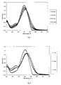
- Changes to solutions of organic semiconductors can e.g. through optical Methods, for example, can be determined by recording a UV / Vis spectrum.
- Holdcroft et. al. were able to show that by adding anthracene, which acts as a scavenger serves for singlet oxygen with the formation of anthraquinone, chain splitting and Shortening the conjugation length when irradiating such poly (3-alkylthiophene) solutions significantly reduced but could not be completely prevented.
- Farther was used to stabilize the complete removal of oxygen from the corresponding Solutions proposed (Macromolecules 1993, 26, 2954-2962).
- the task was therefore to find stable solutions for organic semiconducting compounds to provide, which are suitable for the production of high-quality semiconductor layers.
- organic semiconducting compounds are understood to mean those organic compounds which have an electrical conductivity of at most 10 -2 S / cm, preferably at most 10 -5 S / cm and a charge carrier mobility of at least 10 -5 cm 2 / Vs.
- Charge carrier mobilities are known to the person skilled in the art and can be determined, for example, as described in M.Pope and CESwenberg, Electronic Processes in Organic Crystals and Polymers, 2nd ed., Pp. 709-713 (Oxford University Press, New York Oxford 1999).
- the basic compounds are preferably those that are either easily evaporable or are insoluble or only slightly soluble in the chosen solvent and therefore on easily removed from the organic semiconducting compounds can.
- readily vaporizable basic compounds include those with a boiling point of at most 270 ° C, preferably 50 ° C to 220 ° C, particularly preferably understand 80 to 150 ° C.
- the temperature specifications refer to the Boiling points at atmospheric pressure (1 atm or 1.01325 bar).
- Examples of such basic compounds that are relatively easy to vaporize are primary, secondary or tertiary amines, basic aromatic or aliphatic heterocyclic Compounds or a mixture of two or more of these compounds.
- Such basic compounds are, for example, mono-, di- or trialkylamines, preferably those that are soluble in the solvents used.
- These are, for example n-alkylamines, e.g. Methylamine, ethylamine, propylamine, butylamine, pentylamine, Hexylamine, heptylamine, octylamine, nonylamine, decylamine or dodecylamine, Dialkylamines, e.g. Diethylamine or diisopropylamine, trialkylamines, e.g.
- Trimetylamine dimethylethylamine, triethylamine, tripropylamine, tributhylamine, tripentylamine or trihexylamine, or mixtures thereof, e.g. a mixture of n- or tert-butylamine.
- exemplary of optionally substituted aromatic or optionally substituted saturated or unsaturated aliphatic heterocyclic compounds with 5 to 20 ring C atoms and 1 to 3 identical or different ring heteroatoms the groups nitrogen, oxygen and sulfur are pyridine, pyrazole, pyrazine, pyridazine, Pyrimidine, pyrrole and 3-pyrroline called.
- the preceding lists serve only the exemplary explanation of the invention and are not intended to be exhaustive understand.
- Suitable substituents for R 1 , R 2 and R 3 are, for example, linear or branched C 1 -C 20 alkyl radicals, C 5 -C 12 cycloalkyl radicals or C 6 -C 14 aryl radicals.
- the basic compounds are in a stable solution in a concentration of 0.001% by weight to 20% by weight, preferably from 0.01% by weight to 5% by weight, particularly preferably contain from 0.1% by weight to 2% by weight.
- Basic compounds that are insoluble or only slightly soluble in the chosen solvent are, for example, alkali or alkaline earth metal hydroxides or carbonates or alkali or Alkaline earth salts of weak acids such as Formic acid, acetic acid, propionic acid etc., or polymers containing basic groups such as e.g. Ion-exchange polymers.
- Ion exchange polymers can, for example, organic anion exchangers such as Polycondensates, e.g. from phenol and formaldehyde, or polymers, e.g. by Copolymerization available from styrene, acrylates or methacrylates and divinylbenzene, which were subsequently functionalized accordingly. But others can too appropriately functionalized macromolecules, such as those of natural origin such as celluloses, dextrans and aragoses can be used.
- As basic groups can such anion exchangers functional basic groups, such as primary have secondary or tertiary amine groups or quaternary ammonium groups. Depending on The type and combination of the functional groups can determine the basicity of the ion exchangers vary.
- strongly basic ion exchangers usually contain quaternary ones Ammonium groups, while weakly basic ion exchangers often the less carry basic primary, secondary and / or tertiary amine groups.
- weakly basic ion exchangers often the less carry basic primary, secondary and / or tertiary amine groups.
- Examples of ion exchangers containing basic groups are those with tertiary ones Amines functionalized macroporous polymers from stryrene and divinylbenzene like them e.g. are sold under the trade name Lewatit® by Bayer AG, Leverkusen.
- Organic semiconducting compounds include organic in the context of the invention understand semiconducting polymers.
- polymers are all Compounds with more than one repeating unit, preferably with 4 to 100,000, particularly preferably with 4 to 100, very particularly preferably with 4 to 10 identical or to understand different repetition units.
- Organic semiconducting polymers with up to 10 repeat units are also known to the person skilled in the art as organic semiconducting Oligomers known, so the term organic semiconducting polymers organic includes semiconducting oligomers.
- the organic semiconducting polymers can be have a defined molecular weight or have a molecular weight distribution. In preferred embodiments of the present invention, the organic ones semiconducting compounds semiconducting oligomers with a defined Molecular weight.
- organic semiconducting compounds semiconducting polymers with a Molecular weight distribution.
- organic semiconducting compounds are in principle those which are known to the person skilled in the art are known.
- polythiophenes for example, optionally substituted polythiophenes, Polyphenylenes, polyfluorenes, copolymers of optionally substituted phenylene, Fluorene, vinylene, thiophene units, such as polyphenylene vinylenes, polyvinyl thienylenes, wherein the copolymers are of two or more different ones from the foregoing listed units can be constructed and the different units alternately, can be distributed in blocks, randomly or in any other way in the copolymer.
- substituents for Ar are linear or branched C 1 -C 20 -alkyl radicals, preferably C 1 -C 12 -alkyl radicals, C 1 -C 20 -alkoxy radicals, linear C 1 -C 20 -alkyl radicals interrupted by one or more O atoms or C 1 -C 6 dioxyalkylene radicals in question. Any substituents (one or more) present on the 2,7-fluorene units are preferably located at the 9 position.
- Suitable substituents for R 5 and R 6 are, for example, linear or branched, optionally substituted C 1 -C 20 -alkyl radicals, optionally substituted C 5 -C 12 -cycloalkyl radicals, optionally substituted C 6 -C 14 -aryl radicals.
- Very particularly preferred organic semiconducting compounds are ⁇ , ⁇ '-dialkyl oligothiophenes, such as. ⁇ , ⁇ '-Dialkylquaterthiophene, ⁇ , ⁇ '-Dialkylquinquethiophene, or ⁇ , ⁇ '-dialkyl exithiophenes, and regioregular poly (3-alkylthiophenes).
- the semiconducting compounds are in a stable solution in a concentration of 0.001% by weight to 10% by weight, preferably from 0.01% by weight to 5% by weight, particularly preferably contain from 0.1% by weight to 1% by weight. Mixtures can also be used various organic semiconducting compounds can be used.
- the preparation of the semiconducting organic compounds is known to the person skilled in the art and can, for example, by coupling organolithium compounds with iron (III) salts according to J. Am. Chem. Soc. 1993, 115, p. 12214, from Grignard compounds (JP-A 02 250 881, EP 1 028 136 A2, J. Chem. Soc., Chem. Commun. 1992, p. 70) or organic zinc compounds (US-A 5,546,889, Synth. Meth. 1993, B. 60, p. 175) in Presence of nickel catalysts by means of oxidative coupling of organolithium Compounds with copper salts (Heterocycles 1983, 20, p. 1937 or not yet published German application DE 10 248 876).
- the solutions according to the invention contain organic semiconducting compounds in addition solvents that dissolve the organic semiconducting compounds.
- the or the Stabilizer (s) dissolve completely or partially in the solvent (s) or - for the case that it is liquid stabilizers - with the solvent or solvents are completely or partially miscible.
- solvents Question which solve the organic semiconducting compounds. Adequate solubility is already given when at least 100 ppm of the organic semiconducting compounds are dissolved in the chosen solvent.
- Solvents organic solvents especially halogenated aromatic or aliphatic compounds, aromatic or aliphatic compounds containing ether or keto groups Compounds or mixtures of two or more of these compounds in Question.
- Preferred solvents are, for example, chlorine-containing compounds such as Chloroform, dichloromethane, 1,2-dichloroethane, chlorobenzene and 1,2,4-trichlorobenzene, aromatic compounds such as benzene, toluene or xylenes, compounds containing ether groups such as diethyl ether, tert. Butyl methyl ether, dioxane or tetrahydrofuran and Compounds containing keto groups, such as acetone or methyl ethyl ketone or mixtures from two or more of these solvents.
- Particularly preferred solvents are Chloroform, chlorobenzene, 1,2,4-trichlorobenzene or toluene, is very particularly preferred Chloroform.
- the solution according to the invention contains at least a solvent which contains both the semiconducting compound and the stabilizer solves.
- the Stabilizer is not released. In such cases, such a procedure can be carried out by Be an advantage in which the stabilizer by simple methods, for example by Decanting or filtration can or should be removed before generating the layer.
- the solutions according to the invention have organic semiconducting compounds the advantage over known non-stabilized solutions that they are stable and themselves even after a long time, i.e. up to several days, weeks or even months, even in Do not change the presence of oxygen.
- the solutions according to the invention are for example at temperatures up to 80 ° C, preferably up to 40 ° C, particularly preferably at Room temperature stable for several days, weeks or even months.
- solutions according to the invention could last at room temperature (23 ° C.) for 14 days and longer Air, i.e. in the presence of oxygen, without significant changes were observed.
- chloroform as a solvent for semiconducting organic compounds is particularly advantageous because, for example Chloroform not only has excellent solvency for semiconducting compounds, but also usually layers, in the production of which chloroform as a solvent was used as such, which are, for example, high Charge mobility or have a high "on / off ratio" (see Appl. Phys. Lett. 1996, B.69, p.4108-4110).
- the organic can either semiconducting compounds dissolved in the solvent and then the stabilizer can be added or, conversely, a solution, mixture or suspension of the stabilizer and then the organic semiconducting compounds be added.
- organic semiconducting polymer and Stabilizer combined and only then mixed with solvent or organic semiconducting polymer, stabilizer and solvent can also be put together at the same time.
- the production can be continuous or discontinuous respectively.
- the solutions according to the invention are particularly suitable for the production of semiconductor layers in active and light-emitting electronic Components such as field effect transistors, organic luminescent diodes, photovoltaic Cells, lasers or sensors.
- the present invention therefore furthermore relates to the use of solutions according to the invention for the production of semiconducting layers.
- the solutions of organic semiconducting compounds according to the invention in the form of layers on suitable substrates for example with electrical or electronic structures provided silicon wafers, polymer films or glass panes applied, wherein the solvent is then evaporated.
- Applying from Solution can be made by the known methods, for example by spraying, dipping, Printing and knife coating, spin coating and ink jet printing.
- the removal of the Basic compound (s) can be applied to the appropriate substrates before applying the solutions or together with the solvent after application. In the event that basic compound (s) boiling higher than the solvent can remove the basic compound (s) also after removing the solvent.
- Both solvent and easily vaporizable basic compound (s) can be removed at reduced pressure or atmospheric pressure. The distance can take place, for example, at room temperature or at an elevated temperature. Prefers the basic compounds become almost complete in the production of the layers removed to achieve particularly good semiconductor properties of the layers. It can but also residual amounts of basic compound (s) remain in the layers.
- the solutions according to the invention can be processed into high-quality semiconducting layers. These preferably have charge mobilities of 10 -3 cm 2 / Vs, particularly preferably 10 -2 cm 2 / Vs. Charge mobilities can be determined, for example, as described in M.Pope and CESwenberg, Electronic Processes in Organic Crystals and Polymers, 2nd ed., Pp. 709-713 (Oxford University Press, New York Oxford 1999).
- the layers according to the invention are particularly suitable for use in active and light-emitting electronic components such as field-effect transistors, organic Luminescent diodes, photovoltaic cells, lasers or sensors.
- the present invention therefore furthermore relates to the use of Layers according to the invention as semiconductors in active and light-emitting electronic Components such as field effect transistors, organic luminescent diodes, photovoltaic cells, lasers or sensors.
- active and light-emitting electronic Components such as field effect transistors, organic luminescent diodes, photovoltaic cells, lasers or sensors.
- the layers according to the invention can be further modified after application, for example by heat treatment, e.g. passing through a liquid crystalline Phase, or for structuring e.g. by laser ablation.
- UV / Vis measurements were carried out with a commercially available UV / Vis spectrometer (Perkin-Elmer Lambda 9) at room temperature (23 ° C). Measurements were taken from fresh Solutions, i.e. directly after production, then at intervals of 15 minutes until 2 hours from production, and then every hour from 7 hours Production and carried out daily after 1 to 9 or 1 to 14 days from production.
Landscapes
- Engineering & Computer Science (AREA)
- Chemical & Material Sciences (AREA)
- Materials Engineering (AREA)
- Manufacturing & Machinery (AREA)
- Thin Film Transistor (AREA)
- Medicinal Preparation (AREA)
- Electroluminescent Light Sources (AREA)
- Application Of Or Painting With Fluid Materials (AREA)
- Organic Low-Molecular-Weight Compounds And Preparation Thereof (AREA)
- Heterocyclic Carbon Compounds Containing A Hetero Ring Having Oxygen Or Sulfur (AREA)
Applications Claiming Priority (2)
| Application Number | Priority Date | Filing Date | Title |
|---|---|---|---|
| DE10324533 | 2003-05-28 | ||
| DE10324533A DE10324533A1 (de) | 2003-05-28 | 2003-05-28 | Stabile Lösungen von organischen halbleitenden Verbindungen |
Publications (3)
| Publication Number | Publication Date |
|---|---|
| EP1482575A2 true EP1482575A2 (fr) | 2004-12-01 |
| EP1482575A3 EP1482575A3 (fr) | 2005-10-05 |
| EP1482575B1 EP1482575B1 (fr) | 2011-11-09 |
Family
ID=33103651
Family Applications (1)
| Application Number | Title | Priority Date | Filing Date |
|---|---|---|---|
| EP04011625A Expired - Lifetime EP1482575B1 (fr) | 2003-05-28 | 2004-05-15 | Solutions stables de matériaux organique semiconducteur |
Country Status (7)
| Country | Link |
|---|---|
| US (1) | US20050012068A1 (fr) |
| EP (1) | EP1482575B1 (fr) |
| JP (1) | JP2005007391A (fr) |
| KR (1) | KR20040103335A (fr) |
| AT (1) | ATE533193T1 (fr) |
| DE (1) | DE10324533A1 (fr) |
| TW (1) | TWI349025B (fr) |
Families Citing this family (6)
| Publication number | Priority date | Publication date | Assignee | Title |
|---|---|---|---|---|
| US7317048B2 (en) * | 2003-01-06 | 2008-01-08 | E.I. Du Pont De Nemours And Company | Variable resistance poly(3,4-ethylenedioxythiophene)/poly(styrene sulfonate) for use in electronic devices |
| KR101312269B1 (ko) | 2007-01-05 | 2013-09-25 | 삼성전자주식회사 | 고분자 태양전지 및 그의 제조방법 |
| JP2009010102A (ja) * | 2007-06-27 | 2009-01-15 | Gunze Ltd | 半導体素子 |
| JP6073216B2 (ja) * | 2010-04-12 | 2017-02-01 | メルク パテント ゲーエムベーハー | 有機電子デバイスを作製するための組成物および方法 |
| US20170267515A1 (en) * | 2016-03-18 | 2017-09-21 | Dusty Road Saddlery And Repair, Llc | Saddle anchor and detachable stirrup system |
| JP2017208552A (ja) * | 2017-06-12 | 2017-11-24 | 日産化学工業株式会社 | 電荷輸送性ワニス |
Family Cites Families (31)
| Publication number | Priority date | Publication date | Assignee | Title |
|---|---|---|---|---|
| US2586414A (en) * | 1946-08-14 | 1952-02-19 | Gen Electric | Trolley for electric power distribution system |
| JP2578881B2 (ja) * | 1987-02-25 | 1997-02-05 | 昭和電工株式会社 | ラジカル重合性組成物 |
| DE3717668A1 (de) * | 1987-05-26 | 1988-12-15 | Hoechst Ag | Elektrisch leitende beschichtungsmasse, verfahren zu ihrer herstellung und ihre verwendung |
| US5286414A (en) * | 1987-05-26 | 1994-02-15 | Hoechst Aktiengesellschaft | Electroconductive coating composition, a process for the production thereof and the use thereof |
| US4886625A (en) * | 1987-10-29 | 1989-12-12 | Miles Inc. | Functionalized conducting polymers and their use in diagnostic devices |
| US5475341A (en) * | 1992-06-01 | 1995-12-12 | Yale University | Sub-nanoscale electronic systems and devices |
| TW278096B (fr) * | 1992-09-24 | 1996-06-11 | Dsm Nv | |
| ATE171560T1 (de) * | 1993-03-09 | 1998-10-15 | Koninkl Philips Electronics Nv | Herstellungsverfahren eines musters von einem elektrisch leitfähigen polymer auf einer substratoberfläche und metallisierung eines solchen musters |
| US5965241A (en) * | 1993-08-25 | 1999-10-12 | Polaroid Corp | Electroluminescent devices and processes using polythiophenes |
| US5556706A (en) * | 1993-10-06 | 1996-09-17 | Matsushita Electric Industrial Co., Ltd. | Conductive layered product and method of manufacturing the same |
| US5583169A (en) * | 1995-03-10 | 1996-12-10 | The Regents Of The University Of California Office Of Technology Transfer | Stabilization of polyaniline solutions through additives |
| JP3865406B2 (ja) * | 1995-07-28 | 2007-01-10 | 住友化学株式会社 | 2,7−アリール−9−置換フルオレン及び9−置換フルオレンオリゴマー及びポリマー |
| JP3327558B2 (ja) * | 1995-11-28 | 2002-09-24 | インターナショナル・ビジネス・マシーンズ・コーポレーション | 有機エレクトロルミネセント・デバイスを改良するために使用される有機/無機合金 |
| US6429282B1 (en) * | 1996-05-31 | 2002-08-06 | The Regents Of The University Of California | Stable, concentrated solutions of polyaniline using amines as gel inhibitors |
| US5853906A (en) * | 1997-10-14 | 1998-12-29 | Xerox Corporation | Conductive polymer compositions and processes thereof |
| KR19990066248A (ko) * | 1998-01-23 | 1999-08-16 | 구본준 | 전압분배방식의 디/에이 변환기 |
| DE19839947A1 (de) * | 1998-09-02 | 2000-03-09 | Bayer Ag | Elektrolumineszierende Anordnungen mit Thiophencarboxylat-Metallkomplexen |
| US6166172A (en) * | 1999-02-10 | 2000-12-26 | Carnegie Mellon University | Method of forming poly-(3-substituted) thiophenes |
| US6498114B1 (en) * | 1999-04-09 | 2002-12-24 | E Ink Corporation | Method for forming a patterned semiconductor film |
| DE10016723A1 (de) * | 2000-04-04 | 2001-10-11 | Bayer Ag | Verfahren zur Herstellung von Dialkoxythiophenen und Alkylendioxythiophenen |
| US20020058271A1 (en) * | 2000-07-07 | 2002-05-16 | Johnson Mark K. | Process for detecting a nucleic acid target |
| US6414164B1 (en) * | 2000-07-12 | 2002-07-02 | International Business Machines Corporation | Synthesis of soluble derivatives of sexithiophene and their use as the semiconducting channels in thin-film filed-effect transistors |
| DE10058116A1 (de) * | 2000-11-22 | 2002-05-23 | Bayer Ag | Polythiophene |
| US6692663B2 (en) * | 2001-02-16 | 2004-02-17 | Elecon, Inc. | Compositions produced by solvent exchange methods and uses thereof |
| US6692662B2 (en) * | 2001-02-16 | 2004-02-17 | Elecon, Inc. | Compositions produced by solvent exchange methods and uses thereof |
| EP1370619B1 (fr) * | 2001-03-10 | 2006-06-21 | MERCK PATENT GmbH | Solutions et dispersions de semi-conducteurs organiques |
| US6623903B2 (en) * | 2001-06-22 | 2003-09-23 | Agfa-Gevaert | Material and method for making an electroconductive pattern |
| US6794220B2 (en) * | 2001-09-05 | 2004-09-21 | Konica Corporation | Organic thin-film semiconductor element and manufacturing method for the same |
| JP3963693B2 (ja) * | 2001-10-15 | 2007-08-22 | 富士通株式会社 | 導電性有機化合物及び電子素子 |
| WO2003087222A1 (fr) * | 2002-04-08 | 2003-10-23 | Elecon, Inc. | Compositions polymeres conductrices presentant une conduction de type n |
| US7098525B2 (en) * | 2003-05-08 | 2006-08-29 | 3M Innovative Properties Company | Organic polymers, electronic devices, and methods |
-
2003
- 2003-05-28 DE DE10324533A patent/DE10324533A1/de not_active Withdrawn
-
2004
- 2004-05-15 EP EP04011625A patent/EP1482575B1/fr not_active Expired - Lifetime
- 2004-05-15 AT AT04011625T patent/ATE533193T1/de active
- 2004-05-26 JP JP2004156607A patent/JP2005007391A/ja active Pending
- 2004-05-26 US US10/853,844 patent/US20050012068A1/en not_active Abandoned
- 2004-05-27 TW TW093115017A patent/TWI349025B/zh not_active IP Right Cessation
- 2004-05-27 KR KR1020040037712A patent/KR20040103335A/ko not_active Abandoned
Also Published As
| Publication number | Publication date |
|---|---|
| DE10324533A1 (de) | 2004-12-16 |
| KR20040103335A (ko) | 2004-12-08 |
| TW200512263A (en) | 2005-04-01 |
| TWI349025B (en) | 2011-09-21 |
| US20050012068A1 (en) | 2005-01-20 |
| ATE533193T1 (de) | 2011-11-15 |
| JP2005007391A (ja) | 2005-01-13 |
| EP1482575A3 (fr) | 2005-10-05 |
| EP1482575B1 (fr) | 2011-11-09 |
Similar Documents
| Publication | Publication Date | Title |
|---|---|---|
| EP1370619B1 (fr) | Solutions et dispersions de semi-conducteurs organiques | |
| EP1716604B1 (fr) | Solutions de semi-conducteurs organiques | |
| EP1339772B1 (fr) | Poudres polymeres dispersibles | |
| EP1719193B1 (fr) | Procede de reticulation de semi-conducteurs organiques | |
| DE60125819T2 (de) | Feldeffekttransistoren und materialien und verfahren zu ihrer herstellung | |
| EP2002492B1 (fr) | Utilisation de radicaux heterocycliques pour le dopage de semi-conducteurs organiques | |
| DE10347856B4 (de) | Halbleiterdotierung | |
| EP1837926A1 (fr) | Radicaux ou diradicaux hétérocycliques, leur dimères, oligomères, polymères, composés spiro et polycycliques. Leur usage dans des semi-conducteurs organiques et dispositifs électroniques. | |
| DE10037391A1 (de) | Strukturierbare Materialien, Verfahren zu deren Herstellung und deren Verwendung | |
| DE112011104381T5 (de) | Halbleitermischung | |
| EP1482575B1 (fr) | Solutions stables de matériaux organique semiconducteur | |
| EP1907446B1 (fr) | Structures de 4,4 -bipyridinium polymeres, formulations destinees a une couche electrochrome active et utilisation | |
| DE3701495A1 (de) | Polymer einer fuenfgliedrigen heterocyclischen verbindung und dessen herstellung | |
| EP1631611B1 (fr) | Polythiophenes semi-conducteurs a haute purete et exempts d'ions, procede de production desdits polythiophenes et leur utilisation pour la fabrication de composants electroniques | |
| WO2009056462A9 (fr) | Procédé de dépôt de couches comportant des polyaromates non polaires | |
| EP2824158B1 (fr) | Copolymère semi-conducteur et son procédé de fabrication, mélange de substances, composant électrique ou électronique et son procédé de fabrication | |
| EP1917666B1 (fr) | Composition comprenant un polymere intrinsequement conducteur qui contient de l'indium | |
| EP3401312B1 (fr) | Procédé de stabilisation de 5-hydroxyméthylfurfural (hmf) | |
| EP1979972A2 (fr) | Électrolyte contenant de l'acide phosphonique | |
| DE60122511T2 (de) | Verfahren zum Zubereiten eines Polymers | |
| DE60015286T2 (de) | Kompensierte sulfonierte Polyaniline und Verfahren zu deren Herstellung | |
| EP1448808B1 (fr) | Procede de fabrication de revetements fins peu solubles | |
| DE2947797A1 (de) | Verfahren zur herstellung elektrisch leitfaehiger polyene und deren verwendung in der elektrotechnik und zur antistatischen ausruestung von kunststoffen | |
| DE102024001802A1 (de) | Nickelmonoxid als lochleitendes Material, Perowskit-Solarzelle und Verfahren zur Herstellung von Nickelmonoxid als lochleitendes Material | |
| WO2025172225A1 (fr) | Tranche de silicium recyclable et procédé de recyclage |
Legal Events
| Date | Code | Title | Description |
|---|---|---|---|
| PUAI | Public reference made under article 153(3) epc to a published international application that has entered the european phase |
Free format text: ORIGINAL CODE: 0009012 |
|
| AK | Designated contracting states |
Kind code of ref document: A2 Designated state(s): AT BE BG CH CY CZ DE DK EE ES FI FR GB GR HU IE IT LI LU MC NL PL PT RO SE SI SK TR |
|
| AX | Request for extension of the european patent |
Extension state: AL HR LT LV MK |
|
| PUAL | Search report despatched |
Free format text: ORIGINAL CODE: 0009013 |
|
| AK | Designated contracting states |
Kind code of ref document: A3 Designated state(s): AT BE BG CH CY CZ DE DK EE ES FI FR GB GR HU IE IT LI LU MC NL PL PT RO SE SI SK TR |
|
| AX | Request for extension of the european patent |
Extension state: AL HR LT LV MK |
|
| RIC1 | Information provided on ipc code assigned before grant |
Ipc: 7H 01L 51/40 B Ipc: 7H 01L 51/30 A Ipc: 7C 08G 61/12 B |
|
| 17P | Request for examination filed |
Effective date: 20060405 |
|
| AKX | Designation fees paid |
Designated state(s): AT BE BG CH CY CZ DE DK EE ES FI FR GB GR HU IE IT LI LU MC NL PL PT RO SE SI SK TR |
|
| RAP1 | Party data changed (applicant data changed or rights of an application transferred) |
Owner name: H.C. STARCK GMBH & CO. KG |
|
| RAP1 | Party data changed (applicant data changed or rights of an application transferred) |
Owner name: H.C. STARCK GMBH |
|
| 17Q | First examination report despatched |
Effective date: 20090224 |
|
| RAP1 | Party data changed (applicant data changed or rights of an application transferred) |
Owner name: H.C. STARCK CLEVIOS GMBH |
|
| GRAP | Despatch of communication of intention to grant a patent |
Free format text: ORIGINAL CODE: EPIDOSNIGR1 |
|
| RAP1 | Party data changed (applicant data changed or rights of an application transferred) |
Owner name: HERAEUS CLEVIOS GMBH |
|
| GRAS | Grant fee paid |
Free format text: ORIGINAL CODE: EPIDOSNIGR3 |
|
| GRAA | (expected) grant |
Free format text: ORIGINAL CODE: 0009210 |
|
| AK | Designated contracting states |
Kind code of ref document: B1 Designated state(s): AT BE BG CH CY CZ DE DK EE ES FI FR GB GR HU IE IT LI LU MC NL PL PT RO SE SI SK TR |
|
| REG | Reference to a national code |
Ref country code: GB Ref legal event code: FG4D Free format text: NOT ENGLISH |
|
| REG | Reference to a national code |
Ref country code: CH Ref legal event code: EP |
|
| REG | Reference to a national code |
Ref country code: IE Ref legal event code: FG4D Free format text: LANGUAGE OF EP DOCUMENT: GERMAN |
|
| RAP2 | Party data changed (patent owner data changed or rights of a patent transferred) |
Owner name: HERAEUS PRECIOUS METALS GMBH & CO. KG |
|
| REG | Reference to a national code |
Ref country code: DE Ref legal event code: R096 Ref document number: 502004013037 Country of ref document: DE Effective date: 20111229 |
|
| REG | Reference to a national code |
Ref country code: GB Ref legal event code: 732E Free format text: REGISTERED BETWEEN 20120112 AND 20120118 |
|
| REG | Reference to a national code |
Ref country code: NL Ref legal event code: VDEP Effective date: 20111109 |
|
| PG25 | Lapsed in a contracting state [announced via postgrant information from national office to epo] |
Ref country code: PL Free format text: LAPSE BECAUSE OF FAILURE TO SUBMIT A TRANSLATION OF THE DESCRIPTION OR TO PAY THE FEE WITHIN THE PRESCRIBED TIME-LIMIT Effective date: 20111109 Ref country code: GR Free format text: LAPSE BECAUSE OF FAILURE TO SUBMIT A TRANSLATION OF THE DESCRIPTION OR TO PAY THE FEE WITHIN THE PRESCRIBED TIME-LIMIT Effective date: 20120210 Ref country code: PT Free format text: LAPSE BECAUSE OF FAILURE TO SUBMIT A TRANSLATION OF THE DESCRIPTION OR TO PAY THE FEE WITHIN THE PRESCRIBED TIME-LIMIT Effective date: 20120309 Ref country code: NL Free format text: LAPSE BECAUSE OF FAILURE TO SUBMIT A TRANSLATION OF THE DESCRIPTION OR TO PAY THE FEE WITHIN THE PRESCRIBED TIME-LIMIT Effective date: 20111109 Ref country code: SE Free format text: LAPSE BECAUSE OF FAILURE TO SUBMIT A TRANSLATION OF THE DESCRIPTION OR TO PAY THE FEE WITHIN THE PRESCRIBED TIME-LIMIT Effective date: 20111109 Ref country code: SI Free format text: LAPSE BECAUSE OF FAILURE TO SUBMIT A TRANSLATION OF THE DESCRIPTION OR TO PAY THE FEE WITHIN THE PRESCRIBED TIME-LIMIT Effective date: 20111109 |
|
| REG | Reference to a national code |
Ref country code: IE Ref legal event code: FD4D |
|
| PG25 | Lapsed in a contracting state [announced via postgrant information from national office to epo] |
Ref country code: CY Free format text: LAPSE BECAUSE OF FAILURE TO SUBMIT A TRANSLATION OF THE DESCRIPTION OR TO PAY THE FEE WITHIN THE PRESCRIBED TIME-LIMIT Effective date: 20111109 |
|
| PG25 | Lapsed in a contracting state [announced via postgrant information from national office to epo] |
Ref country code: SK Free format text: LAPSE BECAUSE OF FAILURE TO SUBMIT A TRANSLATION OF THE DESCRIPTION OR TO PAY THE FEE WITHIN THE PRESCRIBED TIME-LIMIT Effective date: 20111109 Ref country code: IE Free format text: LAPSE BECAUSE OF FAILURE TO SUBMIT A TRANSLATION OF THE DESCRIPTION OR TO PAY THE FEE WITHIN THE PRESCRIBED TIME-LIMIT Effective date: 20111109 Ref country code: BG Free format text: LAPSE BECAUSE OF FAILURE TO SUBMIT A TRANSLATION OF THE DESCRIPTION OR TO PAY THE FEE WITHIN THE PRESCRIBED TIME-LIMIT Effective date: 20120209 Ref country code: DK Free format text: LAPSE BECAUSE OF FAILURE TO SUBMIT A TRANSLATION OF THE DESCRIPTION OR TO PAY THE FEE WITHIN THE PRESCRIBED TIME-LIMIT Effective date: 20111109 Ref country code: CZ Free format text: LAPSE BECAUSE OF FAILURE TO SUBMIT A TRANSLATION OF THE DESCRIPTION OR TO PAY THE FEE WITHIN THE PRESCRIBED TIME-LIMIT Effective date: 20111109 Ref country code: EE Free format text: LAPSE BECAUSE OF FAILURE TO SUBMIT A TRANSLATION OF THE DESCRIPTION OR TO PAY THE FEE WITHIN THE PRESCRIBED TIME-LIMIT Effective date: 20111109 |
|
| PG25 | Lapsed in a contracting state [announced via postgrant information from national office to epo] |
Ref country code: RO Free format text: LAPSE BECAUSE OF FAILURE TO SUBMIT A TRANSLATION OF THE DESCRIPTION OR TO PAY THE FEE WITHIN THE PRESCRIBED TIME-LIMIT Effective date: 20111109 Ref country code: IT Free format text: LAPSE BECAUSE OF FAILURE TO SUBMIT A TRANSLATION OF THE DESCRIPTION OR TO PAY THE FEE WITHIN THE PRESCRIBED TIME-LIMIT Effective date: 20111109 |
|
| PLBE | No opposition filed within time limit |
Free format text: ORIGINAL CODE: 0009261 |
|
| STAA | Information on the status of an ep patent application or granted ep patent |
Free format text: STATUS: NO OPPOSITION FILED WITHIN TIME LIMIT |
|
| 26N | No opposition filed |
Effective date: 20120810 |
|
| REG | Reference to a national code |
Ref country code: DE Ref legal event code: R097 Ref document number: 502004013037 Country of ref document: DE Effective date: 20120810 |
|
| PG25 | Lapsed in a contracting state [announced via postgrant information from national office to epo] |
Ref country code: MC Free format text: LAPSE BECAUSE OF NON-PAYMENT OF DUE FEES Effective date: 20120531 |
|
| REG | Reference to a national code |
Ref country code: CH Ref legal event code: PL |
|
| PG25 | Lapsed in a contracting state [announced via postgrant information from national office to epo] |
Ref country code: LI Free format text: LAPSE BECAUSE OF NON-PAYMENT OF DUE FEES Effective date: 20120531 Ref country code: CH Free format text: LAPSE BECAUSE OF NON-PAYMENT OF DUE FEES Effective date: 20120531 |
|
| PG25 | Lapsed in a contracting state [announced via postgrant information from national office to epo] |
Ref country code: ES Free format text: LAPSE BECAUSE OF FAILURE TO SUBMIT A TRANSLATION OF THE DESCRIPTION OR TO PAY THE FEE WITHIN THE PRESCRIBED TIME-LIMIT Effective date: 20120220 |
|
| PG25 | Lapsed in a contracting state [announced via postgrant information from national office to epo] |
Ref country code: FI Free format text: LAPSE BECAUSE OF FAILURE TO SUBMIT A TRANSLATION OF THE DESCRIPTION OR TO PAY THE FEE WITHIN THE PRESCRIBED TIME-LIMIT Effective date: 20111109 |
|
| REG | Reference to a national code |
Ref country code: AT Ref legal event code: MM01 Ref document number: 533193 Country of ref document: AT Kind code of ref document: T Effective date: 20120515 |
|
| PG25 | Lapsed in a contracting state [announced via postgrant information from national office to epo] |
Ref country code: AT Free format text: LAPSE BECAUSE OF NON-PAYMENT OF DUE FEES Effective date: 20120515 |
|
| PGFP | Annual fee paid to national office [announced via postgrant information from national office to epo] |
Ref country code: GB Payment date: 20130521 Year of fee payment: 10 Ref country code: DE Payment date: 20130522 Year of fee payment: 10 |
|
| PGFP | Annual fee paid to national office [announced via postgrant information from national office to epo] |
Ref country code: FR Payment date: 20130603 Year of fee payment: 10 Ref country code: BE Payment date: 20130521 Year of fee payment: 10 |
|
| PG25 | Lapsed in a contracting state [announced via postgrant information from national office to epo] |
Ref country code: TR Free format text: LAPSE BECAUSE OF FAILURE TO SUBMIT A TRANSLATION OF THE DESCRIPTION OR TO PAY THE FEE WITHIN THE PRESCRIBED TIME-LIMIT Effective date: 20111109 |
|
| PG25 | Lapsed in a contracting state [announced via postgrant information from national office to epo] |
Ref country code: LU Free format text: LAPSE BECAUSE OF NON-PAYMENT OF DUE FEES Effective date: 20120515 |
|
| PG25 | Lapsed in a contracting state [announced via postgrant information from national office to epo] |
Ref country code: HU Free format text: LAPSE BECAUSE OF FAILURE TO SUBMIT A TRANSLATION OF THE DESCRIPTION OR TO PAY THE FEE WITHIN THE PRESCRIBED TIME-LIMIT Effective date: 20040515 |
|
| REG | Reference to a national code |
Ref country code: DE Ref legal event code: R119 Ref document number: 502004013037 Country of ref document: DE |
|
| GBPC | Gb: european patent ceased through non-payment of renewal fee |
Effective date: 20140515 |
|
| REG | Reference to a national code |
Ref country code: FR Ref legal event code: ST Effective date: 20150130 |
|
| REG | Reference to a national code |
Ref country code: DE Ref legal event code: R119 Ref document number: 502004013037 Country of ref document: DE Effective date: 20141202 |
|
| PG25 | Lapsed in a contracting state [announced via postgrant information from national office to epo] |
Ref country code: DE Free format text: LAPSE BECAUSE OF NON-PAYMENT OF DUE FEES Effective date: 20141202 |
|
| PG25 | Lapsed in a contracting state [announced via postgrant information from national office to epo] |
Ref country code: FR Free format text: LAPSE BECAUSE OF NON-PAYMENT OF DUE FEES Effective date: 20140602 Ref country code: GB Free format text: LAPSE BECAUSE OF NON-PAYMENT OF DUE FEES Effective date: 20140515 |
|
| PG25 | Lapsed in a contracting state [announced via postgrant information from national office to epo] |
Ref country code: BE Free format text: LAPSE BECAUSE OF NON-PAYMENT OF DUE FEES Effective date: 20140531 |