EP1482562A2 - Vertical mosfet - Google Patents
Vertical mosfet Download PDFInfo
- Publication number
- EP1482562A2 EP1482562A2 EP04253126A EP04253126A EP1482562A2 EP 1482562 A2 EP1482562 A2 EP 1482562A2 EP 04253126 A EP04253126 A EP 04253126A EP 04253126 A EP04253126 A EP 04253126A EP 1482562 A2 EP1482562 A2 EP 1482562A2
- Authority
- EP
- European Patent Office
- Prior art keywords
- gate
- sgt
- silicon pillar
- semiconductor device
- conductor
- Prior art date
- Legal status (The legal status is an assumption and is not a legal conclusion. Google has not performed a legal analysis and makes no representation as to the accuracy of the status listed.)
- Withdrawn
Links
Images






Classifications
-
- H—ELECTRICITY
- H10—SEMICONDUCTOR DEVICES; ELECTRIC SOLID-STATE DEVICES NOT OTHERWISE PROVIDED FOR
- H10D—INORGANIC ELECTRIC SEMICONDUCTOR DEVICES
- H10D30/00—Field-effect transistors [FET]
- H10D30/60—Insulated-gate field-effect transistors [IGFET]
- H10D30/67—Thin-film transistors [TFT]
- H10D30/6757—Thin-film transistors [TFT] characterised by the structure of the channel, e.g. transverse or longitudinal shape or doping profile
-
- H—ELECTRICITY
- H10—SEMICONDUCTOR DEVICES; ELECTRIC SOLID-STATE DEVICES NOT OTHERWISE PROVIDED FOR
- H10P—GENERIC PROCESSES OR APPARATUS FOR THE MANUFACTURE OR TREATMENT OF DEVICES COVERED BY CLASS H10
- H10P10/00—Bonding of wafers, substrates or parts of devices
-
- H—ELECTRICITY
- H10—SEMICONDUCTOR DEVICES; ELECTRIC SOLID-STATE DEVICES NOT OTHERWISE PROVIDED FOR
- H10D—INORGANIC ELECTRIC SEMICONDUCTOR DEVICES
- H10D30/00—Field-effect transistors [FET]
- H10D30/01—Manufacture or treatment
- H10D30/021—Manufacture or treatment of FETs having insulated gates [IGFET]
- H10D30/031—Manufacture or treatment of FETs having insulated gates [IGFET] of thin-film transistors [TFT]
- H10D30/0321—Manufacture or treatment of FETs having insulated gates [IGFET] of thin-film transistors [TFT] comprising silicon, e.g. amorphous silicon or polysilicon
- H10D30/0323—Manufacture or treatment of FETs having insulated gates [IGFET] of thin-film transistors [TFT] comprising silicon, e.g. amorphous silicon or polysilicon comprising monocrystalline silicon
-
- H—ELECTRICITY
- H10—SEMICONDUCTOR DEVICES; ELECTRIC SOLID-STATE DEVICES NOT OTHERWISE PROVIDED FOR
- H10D—INORGANIC ELECTRIC SEMICONDUCTOR DEVICES
- H10D30/00—Field-effect transistors [FET]
- H10D30/60—Insulated-gate field-effect transistors [IGFET]
- H10D30/67—Thin-film transistors [TFT]
- H10D30/6728—Vertical TFTs
-
- H—ELECTRICITY
- H10—SEMICONDUCTOR DEVICES; ELECTRIC SOLID-STATE DEVICES NOT OTHERWISE PROVIDED FOR
- H10D—INORGANIC ELECTRIC SEMICONDUCTOR DEVICES
- H10D30/00—Field-effect transistors [FET]
- H10D30/60—Insulated-gate field-effect transistors [IGFET]
- H10D30/67—Thin-film transistors [TFT]
- H10D30/6729—Thin-film transistors [TFT] characterised by the electrodes
- H10D30/673—Thin-film transistors [TFT] characterised by the electrodes characterised by the shapes, relative sizes or dispositions of the gate electrodes
Definitions
- the present invention relates to a semiconductor device and, more particularly, to a semiconductor device capable of employing a designing method for a device of nanometer scale.
- MOSFETs with a gate length of 20 nm will be required by the year 2009 for LSIs intended for speed enhancement and by the year 2013 for LSIs intended for consumption power reduction.
- a threshold voltage is lowered
- a subthreshold swing S that decides a switching characteristic is increased and a Drain-Induced Barrier Lowering (DIBL) effect is enhanced.
- DIBL Drain-Induced Barrier Lowering
- the SGT is so constructed that a source, a gate and a drain are arranged perpendicularly to a substrate with the gate surrounding a pillar semiconductor layer.
- the SGT therefore occupies much less area than that a flat-type MOSFET does, and it is highly expected that the SGT will be applied to a DRAM, a Flash EEPROM and a CMOS.
- a pillar semiconductor layer (channel) surrounded by a gate contains a high concentration of impurities for controlling a threshold voltage. It is difficult, however, to increase the impurity concentration of the channel, and thus it is difficult to bring the channel surrounded by the gate to a perfect depletion condition. Further, such problems as a decline in drive current arise due to degradation of carrier mobility in the channel.
- the present invention provides a semiconductor device comprising: a silicon pillar having a high-resistivity region and first and second highly doped regions sandwiching the high-resistivity region therebetween, the high-resistivity region having an impurity concentration of 10 17 cm -3 or less; an insulator surrounding the high-resistivity region; and a conductor surrounding the insulator, wherein the conductor is made of a material which permits a voltage applied to the conductor to control an electric current flowing between the first and second highly doped regions and which has a work function bringing the high-resistivity region to a perfect depletion condition during the flow of the electric current between the first and second highly doped regions.
- the semiconductor device of the present invention with the above constitution has a good stability, achieves both a low off-current and a high on-current and can employ a device-designing method by which an ULSI (ultra large scale integrated circuit) operating at a very high speed and consuming a very low power can be realized, even if a length of the conductor in a direction of a height of the silicon pillar (gate length) is 70 nm or less, particularly 20 nm or less.
- ULSI ultra large scale integrated circuit
- a region of a silicon pillar surrounded by a conductor contains a concentration of impurities as low as 10 17 cm -3 or less (Hereafter, the conductor is referred to as a gate, and the region is referred to as a channel).
- the conductor is referred to as a gate
- the region is referred to as a channel.
- the threshold voltage or the off-current I off is controlled by changing the impurity concentration of the channel, and thus it is difficult to decrease the impurity concentration to 10 17 cm -3 or less.
- a gate voltage applied to start an electric current to flow is referred to as a "threshold voltage,” and the channel is referred to as a "p-type region.”
- an enhancement-type NMOS transistor with a drain current of 0 A at a gate voltage of 0 V is attained by increasing the impurity concentration of the channel, while in the present technique, it is achieved by changing the work function of the gate material.
- the present invention therefore, can reduce the impurity concentration of the channel to as low as 10 17 cm -3 or less, thus increasing the resistivity of the channel, and can realize a high mobility of carriers. Consequently, the present invention can alleviate degradation in drive current.
- the impurity concentration of the channel is preferably 10 10 cm -3 to 1017 cm -3 .
- Exemplary p-type impurities contained in the channel include boron and boron fluoride, and exemplary n-type impurities include phosphorus and arsenic.
- the threshold voltage or the off-current I off is determined by changing the work function of the gate material for adjusting the impurity concentration of the channel to 10 17 cm -3 or less.
- the gate material is not particularly limited so long as it has a desired work function. Examples of the gate material include molybdenum silicide (MoSi 2 ), tungsten silicide (WSi 2 ) and nickel silicide (NiSi 2 ).
- a gate material with a work function of 4.668 eV so that an off-current I off of 10 -12 A/ ⁇ m is realized when the silicon pillar has a diameter of 10 nm, the gate length is 20 nm and the thickness (oxide-film equivalent thickness) of the insulator (gate insulating film) is 1 nm.
- Molybdenum silicide may be mentioned as such a material.
- a gate material with a work function of 4.789 eV so that an off-current I off of 10 -12 A/ ⁇ m is realized when the silicon pillar diameter is 10 nm, the gate length is 20 nm and the thickness (oxide-film equivalent thickness) of the insulator is 1 nm.
- Molybdenum silicide may be mentioned as such a material.
- Molybdenum silicide can vary the work function from 4.6 eV to 4.8 eV.
- the work function of molybdenum silicide may be adjusted by changing the constituent ratio of molybdenum to silicon or by changing, before silicification, the concentration of impurities doped in polysilicon.
- the channel is formed as a high-resistivity region containing a concentration of impurities of 10 17 cm -3 or less
- punchthrough may occur to degrade a controllability of the gate over the channel so that a stable operation is prevented.
- the silicon pillar diameter thickness in the case of a prism silicon pillar
- controlling the silicon pillar diameter assists the gate length to be reduced significantly according to scaling rules.
- the silicon pillar diameter is preferably 0.7 to 35nm, and where the gate length is 20 nm or less, the gate length is preferably 0.2 to 10 nm.
- the subthreshold swing S that decides the switching characteristic will have an ideal value.
- the off-current can be reduced, resulting in a semiconductor device capable of operating with a high current.
- the present invention can provide a semiconductor device capable of realizing such scaling to a gate length of 70 nm or less, particularly 20 nm or less that permits the semiconductor device to operate at a high speed and also to consume a low power. Further, the present invention can be applied not only to a semiconductor device with a gate length of 70 nm or less but also to a semiconductor device with a gate length of more than 70 nm.
- the present semiconductor device comprises a silicon pillar having a high-resistivity region (channel) and first and second highly doped regions (source/drain) sandwiching the high-resistivity region therebetween; an insulator (gate insulating film) surrounding the high-resistivity region and a conductor (gate) surrounding the insulator.
- the gate permits a voltage applied thereto to control an electric current flowing between the source/drain.
- impurities are usable for the source/drain as for the channel, and usually, impurities doped into the source/drain have a conductivity-type opposite to that of impurities doped into the channel.
- the impurity concentrations of the source/drain each are about 10 18 cm -3 to 10 22 cm -3 , though they vary depending on desired characteristics of the semiconductor device,
- the gate insulating film is not particularly limited, therefore a known material can be used for its film.
- Examples of such a gate insulating film include films with a high dielectric constant such as a silicon oxide film, a silicon nitride film, a laminate film of these films (more specifically, an ONO film, etc.), a silicon oxynitride film, an aluminum oxide film, a titanium oxide film, a tantalum oxide film and a hafnium oxide film.
- the thickness (oxide-film equivalent thickness) of the gate insulating film is preferably 0.1 to 10 nm.
- the shape and the size of the silicon pillar are not particularly limited, and may be any necessary to provide a semiconductor device having desired characteristics. Examples of the shape include cylinder, prism (in the case of prism, the silicon pillar may have a triangle, square or polygon cross-section taken along the substrate) and conifer. Further, a plurality of semiconductor devices may be arranged in one silicon pillar. In such a case, the silicon pillar has a height that permits the plurality of semiconductor devices to exist.
- the silicon pillar preferably has a diameter half the gate length or smaller, and more preferably, has a diameter ranging from one-hundredth of the gate length or greater to half the gate length or smaller.
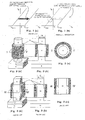
- Fig. 2(a) is a schematic bird's-eye view of the semiconductor device (SGT structure of perfect-depletion type) of the present invention.
- Fig. 2(b) is a schematic cross-section taken along a channel length direction of the semiconductor device illustrated in Fig. 2(a).
- Fig. 2(c) is a schematic cross-section taken along cut-line I-I' of Fig. 2(a).
- the semiconductor device of Fig. 2(a) comprises a silicon oxide film 6, a silicon pillar formed on the silicon oxide film 6, a gate insulating film 2, and a gate 1 surrounding the gate insulating film 2.
- the silicon pillar includes a first highly doped region 3, a high-resistivity region 4 having an impurity concentration of 10 17 cm -3 or less, and a second highly doped region 5.
- the high-resistivity region 4 is surrounded by the gate insulating film 2.
- a current flowing between the first highly doped region 3 and the second highly doped region 5 is controlled by a voltage applied to the gate 1.
- the gate 1 is made of a material having a work function which enables the high-resistivity region 4 to be perfectly depleted while an electric current is flowing between the first highly doped region 3 and the second highly doped region 5.
- the present invention will be explained with reference to this semiconductor device of Fig. 2(a) as an example.
- Fig. 3(a) is a schematic bird's-eye view of the Fin FET to be compared.
- Fig. 3(b) is a schematic cross-section taken along a channel length direction of the Fin FET illustrated in Fig. 3(a).
- Fig. 3(c) is a schematic cross-section taken along cut-line II-II' of Fig. 3(a).
- Fig. 3(a) is a schematic bird's-eye view of the Fin FET to be compared.
- Fig. 3(b) is a schematic cross-section taken along a channel length direction of the Fin FET illustrated in Fig. 3(a).
- Fig. 3(c) is a schematic cross-section taken along cut-line II-II' of Fig. 3(a).
- reference numeral 7 denotes a gate
- 8 denotes a gate insulating film
- 9 denotes a first highly doped region
- 10 denotes a high-resistivity region of rectangular parallelepiped having an impurity concentration of 10 17 cm -3 or less
- 11 denotes a second highly doped region
- 12 denotes a silicon oxide film.
- the first highly doped region 9, the high-resistivity region 10 of rectangular parallelepiped and the second highly doped region 11 constitute a silicon pillar.
- the semiconductor device of the present invention is referred to as a Body Intrinsic Surrounding Gate Transistor (BI-SGT), while the Fin FET for comparison with the semiconductor device of the present invention is called a Body Intrinsic Double Gate MOSFET (BI-DG).
- BI-SGT Body Intrinsic Surrounding Gate Transistor
- BI-DG Body Intrinsic Double Gate MOSFET
- the impurity concentrations of the high-resistivity region 4 (BI-SGT) and the high-resistivity region 10 of rectangular parallelepiped (BI-DG) be each set to 10 17 cm -3 or less so that decrease in mobility of carriers in the respective devices is inhibited. In the three-dimensional device simulation, it is assumed that the impurity concentrations of the high resistivity regions are zero.
- the gate 1 (BI-SGT) and the gate 7 (BI-DG) are each a metal gate or a metal silicide gate.
- the gate insulating film 2 (BI-SGT) and the gate insulating film 8 (BI-DG) each have a thickness of 1 nm. This value of 1 nm, which is an oxide-film equivalent thickness, is appropriate in terms of the generation of a gate length of 20 nm, and it is more preferable to use a film having a higher dielectric constant so that the gate insulating film can have a greater physical thickness.
- Electric characteristics of the BI-SGT and the BI-DG are evaluated by conducting the three-dimensional device simulation on the BI-SGT and the BI-DG each with gate lengths of 10, 20, 30, 40, 50, 60, 70, 80, 90, 100 and 200 nm for each of the lengths of the gate 1 (gate length of the BI-SGT) and the gate 7 (gate length of the BI-DG) when the diameter of a region of the silicon pillar corresponding to the high-resistivity region 4 (hereafter, referred to simply as the silicon pillar diameter) (BI-SGT) and the thickness of a region of the silicon pillar corresponding to the high-resistivity region 10 of rectangular parallelepiped (hereafter, referred to simply as the silicon pillar thickness) (BI-DG) are each 5 nm, 10 nm and 25 nm.
- the results of the three-dimensional device simulation show that the BI-SGT has excellent characteristic to inhibit the short-channel effect and on-current Ion versus off-current
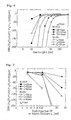
- Fig. 4 is a graph illustrating the dependence of threshold voltage on gate length in each of the BI-SGT and the BI-DG.
- Fig. 5 is a graph illustrating the dependence of subthreshold swing S on gate length in each of the BI-SGT and the BI-DG.
- Fig. 6 is a graph illustrating the dependence of DIBL effect on gate length in each of the BI-SGT and the BI-DG.
- the silicon pillar diameter (BI-SGT) and the silicon pillar thickness (BI-DG) are 5 nm, 10 nm and 25 nm, while the oxide-film equivalent thicknesses of the gate insulating film 2 (BI-SGT) and the gate insulating film 8 (BI-DG) are each 1 nm.
- a threshold voltage shift ⁇ V th has a reference value of zero when the silicon pillar diameter (BI-SGT) is 5 nm.
- the DIBL effect is expressed in a value (DIBL effect value) given by subtracting a threshold voltage obtained at a drain voltage of 0.05 V from a threshold voltage obtained at a drain voltage of 1 V.
- Fig. 4 shows that both the BI-SGT and the BI-DG increase the threshold voltage shift ⁇ V th with reducing gate length, but also that, when the silicon pillar diameter of the BI-SGT is the same as the silicon pillar thickness of the BI-DG, the BI-SGT inhibits a lowering of the threshold voltage more greatly than the BI-DG by one generation of gate length.
- the BI-SGT shows excellent characteristics, i.e., a subthreshold swing S of 63 mV/dec and a DIBL effect value of -17 mV where the gate length is 20 nm and the silicon pillar diameter is 10 nm (see: black dots ⁇ in Figs 5 and 6).
- the BI-DG shows a subthreshold swing S of 77 mV/dec and a DIBL effect value of -75 mV where the silicon pillar thickness is 10 nm (see: white dots ⁇ in Figs 5 and 6).
- the BI-SGT has a minimum gate length of 20 nm while the BI-DG has a minimum gate length of 30 nm when the silicon pillar diameter (BI-SGT) and the silicon pillar thickness (BI-DG) are each 10 nm.
- the BI-SGT in which the channel is surrounded by the gate has a higher controllability of the gate over the channel than the BI-DG in which the channel is interposed between the gates.
- the BI-SGT therefore, can more effectively inhibit the short-channel effect (i.e., lowering of threshold voltage, degradation in subthreshold swing S, increase in DIBL effect and the like generated when the gate length becomes shorter), and can realize more aggressive scaling of the gate length than the BI-DG.
- the BI-SGT with a gate length L may be so designed that the silicon pillar diameter is half the gate length L or smaller where the gate insulating film has an oxide-film equivalent thickness of 1 nm.
- the BI-DG on the other hand, must be so designed that the silicon pillar thickness is one thirds of the gate length L. This means that the BI-DG needs to meet severer process requirements than the BI-SGT when the BI-DG is intended to realize the same gate length as the BI-SGT.
- Fig. 7 is a graph illustrating the dependence of DIBL effect on each of silicon pillar diameter (BI-SGT) and silicon pillar thickness (BI-DG).
- the gate lengths of the BI-SGT and the BI-DG each are 20 nm, 30 nm and 40 nm.
- Fig. 7 shows that each of the BI-SGT and BI-DG reduces the DIBL effect with decreasing silicon pillar diameter (BI-SGT) or silicon pillar thickness (BI-DG). More specifically, by decreasing the silicon pillar diameter (BI-SGT) or silicon pillar thickness (BI-DG), capacities between the source/drain and channel are each decreased, and thereby the controllability of the channel over the gate can be improved. Thus, decreasing the silicon pillar diameter (BI-SGT) or silicon pillar thickness (BI-DG) is critically important in inhibiting the short-channel effect.
- the BI-SGT employs a cylindrical silicon pillar
- the BI-SGT has a higher controllability of the channel over the gate than the BI-DG whose silicon pillar is of rectangular parallelepiped and can inhibit the DIBL effect more effectively than the BI-DG.
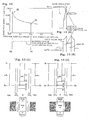
- Figs. 8 and 9 are graphs illustrating the drain current versus gate voltage characteristics (I d -V g characteristics).
- Fig. 8 is plotted with a log scale and
- Fig. 9 is plotted with a linear scale.
- the gate length is 20 nm and the silicon pillar diameter is 10 nm
- the gate length is 20 nm and the silicon pillar thickness is 10 nm.
- the off-current I off is defined as a drain current per unit channel width obtained when the gate voltage Vg is 0 V
- the on-current Ion is defined as a drain current per unit channel width obtained when the gate voltage V g and the drain voltage V d each are 1 V. This time, the off-current I off is set to 1 nA/ ⁇ m in both the BI-SGT and the BI-DG.
- the on-current Ion of the BI-STG is 1.24 times as large as that of the BI-DG (see Fig. 9).
- the BI-STG has a subthreshold swings S of 63 mV/dec, while the BI-DG has a subthreshold swings S of 77 mV/dec (see Fig. 8).
- the high drive-performance of the BI-SGT is attributed to the almost ideal subthreshold swing S (an ideal subthreshold swing S indicative of perfect depletion is 60 mV/dec). Therefore, the BI-SGT can realize a CMOS design with high speed and low power consumption.
- Fig. 10 is a graph illustrating the on-current Ion versus off-current I off characteristics in the BI-SGT and the BI-DG. More specifically, Fig. 10 shows the dependence of on-current Ion on off-current I off in each of the BI-SGT and the BI-DG.
- the silicon pillar diameter is 10 nm
- the oxide-film equivalent thickness of the gate insulating film is 1 nm
- the gate length is 20 nm and the drain voltage is 1 V
- the silicon pillar thickness is 10 nm
- the oxide-film equivalent thickness of the gate insulating film is 1 nm
- the gate length is 20 nm and the drain voltage is 1 V.
- on-current Ion of the BI-SGT can be compare with on-current Ion of the BI-DG when the BI-SGT and the BI-DG have the same off-current I off .
- the off-current I off is 10 -12 A/ ⁇ m, for instance, the on-current Ion of the BI-SGT is 1.52 times as large as that of the BI-DG. This is due to the fact that while the BI-SGT has the almost ideal subthreshold swing S, the BI-DG has the subthreshold swing S of 77 mV/dec.
- the off-current I off As the off-current I off is increased, the difference in on-current Ion between the BI-SGT and the BI-DG narrows.
- the off-current I off is 10 -6 A / ⁇ m
- the on-current I on of the BI-SGT is only 1.05 times as large as that of the BI-DG, since if the BI-SGT is designed to provide such a high off-current I off , it becomes difficult for the BI-SGT to obtain an ideal subthreshold swing S in a subthreshold region.
- the merits of the BI-SGT can be fully utilized. Also, by using the BI-SGT, a high on-current I on of 1170 ⁇ A/ ⁇ m can be realized together with a low off-current I off of 10 -12 A/ ⁇ m. Thus, the BI-SGT can provide a CMOS design with high speed and low power consumption.
- Fig. 11 is a graph illustrating a relation of the gate work function and the off-current in each of the BI-SGT and the BI-DG.
- the silicon pillar diameter is 10 nm
- the oxide-film equivalent thickness of the gate insulating film is 1 nm
- the gate length is 20 nm and the drain voltage is 1 V
- the silicon pillar thickness is 10 nm
- the oxide-film equivalent thickness of the gate insulating film is 1 nm
- the gate length is 20 nm and the drain voltage is 1 V.
- Fig. 11 shows that, by employing a gate material with a work function ranging from 4.2 eV to 4.8 eV, the BI-SGT with a gate length of 20 nm can be realized.
- a gate material with a work function of 4.668 eV may be used when, in the NMOSFET, the silicon pillar diameter is 10 nm, the oxide-film equivalent thickness of the gate insulating film is 1 nm, and the gate length is 20 nm.
- Examples of such a gate material include molybdenum silicide (MoSi 2 ).
- a gate material with a work function of 4.789 eV may be used when, in the PMOSFET, the silicon pillar diameter is 10 nm, the oxide-film equivalent thickness of the gate insulating film is 1 nm, and the gate length is 20 nm.
- Examples of such a gate material include molybdenum silicide (MoSi 2 ).
- Molybdenum silicide (MoSi 2 ) can vary the work function from 4.6 eV to 4.8 eV.
- the threshold voltage or the off-current I off in the BI-SGT can be determined by the work function of the gate.
- Fig. 12 is a graph illustrating the relation between the surface electric field and the electron mobility of a MOSFET structure.
- Fig. 12(A) is a band-gap diagram showing that a charge-neutral region is created in a p-type region (high resistivity region) when an applied gate voltage equal to or greater than the threshold voltage causes the electric current to flow.
- Fig. 12(B) is a band-gap diagram showing that the p-type region is perfectly depleted when the applied gate voltage equal to or greater than the threshold voltage causes the electric current to flow.
- the surface electric field of the MOS structure means an electric field that is applied in a direction perpendicular to the interface between the gate oxide film and the channel in the SGT structure of perfect-depletion type of the present invention shown in the schematic cross-section of Fig. 2(b).
- Fig. 12 shows that electron mobility increases with decreasing surface electric field of the MOS structure.
- the BI-SGT of the present invention compare the case where a charge-neutral region is created in a p-type region (high resistivity region) when an applied gate voltage equal to or greater than the threshold voltage causes the electric current to flow (Fig. 12(A)), with the case where the p-type region is perfectly depleted when an applied gate voltage equal to or greater than the threshold voltage causes the electric current to flow (Fig. 12(B)), the surface electric field of the MOS structure in the former case is smaller than that in the latter case. Therefore, the BI-SGT of the present invention can improve the electron mobility, and as a result, can increase the electric current flowing through the channel, i.e., drive current.
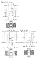
- FIG. 13(4) is an energy-band diagram when a potential of the p - -type region is shifted parallel in response to the gate voltage.
- Fig. 13(5) is an energy-band diagram when the p - -type region is strongly inverted to cause the electric current to flow and when the p - -type region is perfectly depleted.
- a positive gate-voltage is applied, a depletion layer in the p - -type region expands in a concentric configuration to the center of the silicon pillar until the p - -type region is just perfectly depleted (see Fig. 13(3)).
- the applied gate voltage is divided into two and applied to the gate insulating film and to the p - -type region, since electric lines of force emanating from the gate charge is terminated due to ionized impurity atoms present in the p--type region.
- Fig. 14(4) is an energy-band diagram when the potential of the p - -type region is shifted parallel in response to the gate voltage.
- Fig. 14 (5) is an energy-band diagram when the p - -type region is strongly inverted to cause the electric current to flow and when the p - -type region is perfectly depleted.
- Fig. 15(4) is an energy-band diagram when the potential of the p - -type region is shifted parallel in response to the gate voltage.
- Fig. 15 (5) is an energy-band diagram when the p - -type region is strongly inverted to cause the electric current to flow and when the p - -type region is perfectly depleted.
- the present invention can form the channel as a high-resistivity region containing a concentration of impurities of 10 17 cm -3 or less by selecting a work function of the gate material. Therefore, the present invention can easily bring the channel to the perfect depletion condition and can optimize the mobility of carriers. Consequently, the present technique can realize a high drive-current.
- the present invention can inhibit a lowering of threshold voltage, realize an ideal subthreshold swing S and inhibit an enhancement of the DIBL by reducing the diameter of the silicon pillar even if the gate length is scaled down to 70 nm or less, particularly 20 nm or less. Therefore, the present invention can achieve both a low off-current and a high on-current.
- the gate length of the semiconductor device of the present invention is not limited to 70 nm or less.
- the present invention can realize an ULSI operating at a very high speed and consuming a very low power.
Landscapes
- Thin Film Transistor (AREA)
- Insulated Gate Type Field-Effect Transistor (AREA)
- Electrodes Of Semiconductors (AREA)
- Semiconductor Integrated Circuits (AREA)
Abstract
Description

Claims (8)
- A semiconductor device comprising:wherein the conductor is made of a material which permits a voltage applied to the conductor to control an electric current flowing between the first and second highly doped regions and which has a work function bringing the high-resistivity region to a perfect depletion condition during the flow of the electric current between the first and second highly doped regions.a silicon pillar having a high-resistivity region and first and second highly doped regions sandwiching the high-resistivity region therebetween, the high-resistivity region having an impurity concentration of 1017 cm-3 or less;an insulator surrounding the high-resistivity region; anda conductor surrounding the insulator,
- The semiconductor device of claim 1, wherein the high-resistivity region has an impurity concentration of 1010 cm-3 to 1017 cm-3.
- The semiconductor device of claim 1, wherein the conductor is made of a material with a work function ranging from 4.2 eV to 4.8 eV.
- The semiconductor device of claim 3, wherein the conductor is made of MoSi2.
- The semiconductor device of claim 1, wherein the silicon pillar has a diameter half a length of the conductor in a direction of a height of the silicon pillar or smaller.
- The semiconductor device of claim 5, wherein the silicon pillar has a diameter ranging from one-hundredth of the length of the conductor in the direction of the height of the silicon pillar or greater to half the length or smaller.
- The semiconductor device of claim 1, wherein the first and second highly doped regions each have an impurity concentration of 1018 cm-3 to 1022 cm-3.
- A semiconductor device comprising a silicon pillar in which a channel region is disposed lengthwise of the pillar between source and drain regions, wherein a gate insulating film surrounds the channel region, a gate conductor surrounds the gate insulating film, and the gate conductor is arranged to permit a voltage applied thereto to control the flow of an electric current between the source and drain regions.
Applications Claiming Priority (2)
| Application Number | Priority Date | Filing Date | Title |
|---|---|---|---|
| JP2003151177 | 2003-05-28 | ||
| JP2003151177A JP4108537B2 (en) | 2003-05-28 | 2003-05-28 | Semiconductor device |
Publications (2)
| Publication Number | Publication Date |
|---|---|
| EP1482562A2 true EP1482562A2 (en) | 2004-12-01 |
| EP1482562A3 EP1482562A3 (en) | 2005-08-31 |
Family
ID=33128252
Family Applications (1)
| Application Number | Title | Priority Date | Filing Date |
|---|---|---|---|
| EP04253126A Withdrawn EP1482562A3 (en) | 2003-05-28 | 2004-05-27 | Vertical mosfet |
Country Status (5)
| Country | Link |
|---|---|
| US (1) | US20040262681A1 (en) |
| EP (1) | EP1482562A3 (en) |
| JP (1) | JP4108537B2 (en) |
| KR (1) | KR100545161B1 (en) |
| TW (1) | TW200505028A (en) |
Cited By (6)
| Publication number | Priority date | Publication date | Assignee | Title |
|---|---|---|---|---|
| WO2006087044A1 (en) * | 2005-02-21 | 2006-08-24 | Infineon Technologies Ag | Integrated circuit arrangement comprising a field effect transistor, especially a tunnel field effect transistor |
| DE102006044840A1 (en) * | 2006-09-22 | 2008-04-03 | Qimonda Ag | Integrated transistor device has semiconductor substrate, where column is formed in semiconductor substrate, and source or drain area is formed within upper area of column |
| US7642586B2 (en) | 2006-09-08 | 2010-01-05 | Qimonda Ag | Integrated memory cell array |
| EP2718973A4 (en) * | 2011-06-06 | 2015-04-15 | Micron Technology Inc | METHOD FOR PROVIDING A SEMICONDUCTOR MEMORY DEVICE |
| US9379238B2 (en) | 2010-11-26 | 2016-06-28 | Centre National De La Recherche Scientifique (C.N.R.S.) | Process for fabricating a field-effect transistor device implemented on a network of vertical nanowires, the resulting transistor device, an electronic device comprising such transistor devices and a processor comprising at least one such device |
| JP2023146053A (en) * | 2022-03-29 | 2023-10-12 | セイコーエプソン株式会社 | Semiconductor equipment and power devices |
Families Citing this family (128)
| Publication number | Priority date | Publication date | Assignee | Title |
|---|---|---|---|---|
| JP2007158300A (en) * | 2005-12-07 | 2007-06-21 | Korea Electronics Telecommun | Low Schottky barrier through transistor and method of manufacturing the same |
| WO2007106424A2 (en) * | 2006-03-10 | 2007-09-20 | The Trustees Of Boston University | Treating cancers with activated ras through inhibition of pkc delta |
| JP5016832B2 (en) | 2006-03-27 | 2012-09-05 | 株式会社東芝 | Nonvolatile semiconductor memory device and manufacturing method thereof |
| US8354311B2 (en) | 2006-04-04 | 2013-01-15 | Micron Technology, Inc. | Method for forming nanofin transistors |
| US7491995B2 (en) | 2006-04-04 | 2009-02-17 | Micron Technology, Inc. | DRAM with nanofin transistors |
| US8734583B2 (en) | 2006-04-04 | 2014-05-27 | Micron Technology, Inc. | Grown nanofin transistors |
| JP5229587B2 (en) * | 2006-04-04 | 2013-07-03 | マイクロン テクノロジー, インク. | Growth type nano fin transistor |
| EP1900681B1 (en) * | 2006-09-15 | 2017-03-15 | Imec | Tunnel Field-Effect Transistors based on silicon nanowires |
| JP5100080B2 (en) | 2006-10-17 | 2012-12-19 | 株式会社東芝 | Nonvolatile semiconductor memory device and manufacturing method thereof |
| JP5221024B2 (en) * | 2006-11-06 | 2013-06-26 | 株式会社Genusion | Nonvolatile semiconductor memory device |
| JP2008130712A (en) * | 2006-11-20 | 2008-06-05 | Hitachi Maxell Ltd | 3-terminal crystal silicon element |
| JP5130596B2 (en) | 2007-05-30 | 2013-01-30 | 国立大学法人東北大学 | Semiconductor device |
| JP2009004425A (en) * | 2007-06-19 | 2009-01-08 | Elpida Memory Inc | Semiconductor device and manufacturing method of semiconductor device |
| JP2009038201A (en) * | 2007-08-01 | 2009-02-19 | Elpida Memory Inc | Semiconductor device and manufacturing method of semiconductor device |
| JP5466816B2 (en) * | 2007-08-09 | 2014-04-09 | ピーエスフォー ルクスコ エスエイアールエル | Manufacturing method of vertical MOS transistor |
| JP5466818B2 (en) * | 2007-09-27 | 2014-04-09 | ピーエスフォー ルクスコ エスエイアールエル | Semiconductor device |
| TWI459559B (en) * | 2007-10-29 | 2014-11-01 | Unisantis Elect Singapore Pte | Semiconductor structure and method of manufacturing the same |
| US8183628B2 (en) * | 2007-10-29 | 2012-05-22 | Unisantis Electronics Singapore Pte Ltd. | Semiconductor structure and method of fabricating the semiconductor structure |
| US8896056B2 (en) * | 2007-12-05 | 2014-11-25 | Unisantis Electronics Singapore Pte Ltd. | Surrounding gate transistor semiconductor device |
| JP2009141110A (en) * | 2007-12-06 | 2009-06-25 | Elpida Memory Inc | Semiconductor device and manufacturing method of semiconductor device |
| JP5317343B2 (en) | 2009-04-28 | 2013-10-16 | ユニサンティス エレクトロニクス シンガポール プライベート リミテッド | Semiconductor device and manufacturing method thereof |
| US8598650B2 (en) * | 2008-01-29 | 2013-12-03 | Unisantis Electronics Singapore Pte Ltd. | Semiconductor device and production method therefor |
| US7759729B2 (en) * | 2008-02-07 | 2010-07-20 | International Business Machines Corporation | Metal-oxide-semiconductor device including an energy filter |
| US8129763B2 (en) * | 2008-02-07 | 2012-03-06 | International Business Machines Corporation | Metal-oxide-semiconductor device including a multiple-layer energy filter |
| DE102008030853B4 (en) * | 2008-06-30 | 2014-04-30 | Globalfoundries Dresden Module One Limited Liability Company & Co. Kg | Three-dimensional transistor with a dual-channel configuration |
| US7750400B2 (en) * | 2008-08-15 | 2010-07-06 | Texas Instruments Incorporated | Integrated circuit modeling, design, and fabrication based on degradation mechanisms |
| US8278691B2 (en) * | 2008-12-11 | 2012-10-02 | Micron Technology, Inc. | Low power memory device with JFET device structures |
| JP4530098B1 (en) * | 2009-05-29 | 2010-08-25 | 日本ユニサンティスエレクトロニクス株式会社 | Semiconductor device |
| JP5356970B2 (en) | 2009-10-01 | 2013-12-04 | ユニサンティス エレクトロニクス シンガポール プライベート リミテッド | Semiconductor device |
| JP5635256B2 (en) * | 2009-11-24 | 2014-12-03 | ピーエスフォー ルクスコ エスエイアールエルPS4 Luxco S.a.r.l. | Semiconductor device and manufacturing method thereof |
| WO2011111662A1 (en) | 2010-03-08 | 2011-09-15 | 日本ユニサンティスエレクトロニクス株式会社 | Solid-state image pickup device |
| US8487357B2 (en) | 2010-03-12 | 2013-07-16 | Unisantis Electronics Singapore Pte Ltd. | Solid state imaging device having high sensitivity and high pixel density |
| JP5128630B2 (en) * | 2010-04-21 | 2013-01-23 | ユニサンティス エレクトロニクス シンガポール プライベート リミテッド | Semiconductor device |
| JP5066590B2 (en) | 2010-06-09 | 2012-11-07 | ユニサンティス エレクトロニクス シンガポール プライベート リミテッド | Semiconductor device and manufacturing method thereof |
| JP5087655B2 (en) | 2010-06-15 | 2012-12-05 | ユニサンティス エレクトロニクス シンガポール プライベート リミテッド | Semiconductor device and manufacturing method thereof |
| JP2012023305A (en) * | 2010-07-16 | 2012-02-02 | Elpida Memory Inc | Semiconductor device and semiconductor device manufacturing method |
| US20120168819A1 (en) * | 2011-01-03 | 2012-07-05 | Fabio Alessio Marino | Semiconductor pillar power MOS |
| US9401436B2 (en) | 2011-05-05 | 2016-07-26 | Qualcomm Incorporated | Multiple control transcap variable capacitor |
| US8564034B2 (en) | 2011-09-08 | 2013-10-22 | Unisantis Electronics Singapore Pte. Ltd. | Solid-state imaging device |
| US8669601B2 (en) | 2011-09-15 | 2014-03-11 | Unisantis Electronics Singapore Pte. Ltd. | Method for producing semiconductor device and semiconductor device having pillar-shaped semiconductor |
| US8916478B2 (en) | 2011-12-19 | 2014-12-23 | Unisantis Electronics Singapore Pte. Ltd. | Method for manufacturing semiconductor device and semiconductor device |
| US8772175B2 (en) | 2011-12-19 | 2014-07-08 | Unisantis Electronics Singapore Pte. Ltd. | Method for manufacturing semiconductor device and semiconductor device |
| US8748938B2 (en) | 2012-02-20 | 2014-06-10 | Unisantis Electronics Singapore Pte. Ltd. | Solid-state imaging device |
| JP6100559B2 (en) | 2012-03-05 | 2017-03-22 | 株式会社半導体エネルギー研究所 | Semiconductor memory device |
| US9041095B2 (en) * | 2013-01-24 | 2015-05-26 | Unisantis Electronics Singapore Pte. Ltd. | Vertical transistor with surrounding gate and work-function metal around upper sidewall, and method for manufacturing the same |
| US9024376B2 (en) | 2013-01-25 | 2015-05-05 | Unisantis Electronics Singapore Pte. Ltd. | Vertical transistor with dielectrically-isolated work-function metal electrodes surrounding the semiconductor pillar |
| US9112047B2 (en) * | 2013-02-28 | 2015-08-18 | Freescale Semiconductor, Inc. | Split gate non-volatile memory (NVM) cell and method therefor |
| JP5654184B1 (en) | 2013-04-16 | 2015-01-14 | ユニサンティス エレクトロニクス シンガポール プライベート リミテッドUnisantis Electronics Singapore Pte Ltd. | Semiconductor device manufacturing method and semiconductor device |
| WO2014174672A1 (en) | 2013-04-26 | 2014-10-30 | ユニサンティス エレクトロニクス シンガポール プライベート リミテッド | Semiconductor device production method and semiconductor device |
| WO2014203304A1 (en) | 2013-06-17 | 2014-12-24 | ユニサンティス エレクトロニクス シンガポール プライベート リミテッド | Semiconductor device manufacturing method and semiconductor device |
| WO2015008387A1 (en) | 2013-07-19 | 2015-01-22 | ユニサンティス エレクトロニクス シンガポール プライベート リミテッド | Method for manufacturing semiconductor device, and semiconductor device |
| JP5759077B1 (en) | 2013-08-07 | 2015-08-05 | ユニサンティス エレクトロニクス シンガポール プライベート リミテッドUnisantis Electronics Singapore Pte Ltd. | Semiconductor device manufacturing method and semiconductor device |
| WO2015045054A1 (en) | 2013-09-26 | 2015-04-02 | ユニサンティス エレクトロニクス シンガポール プライベート リミテッド | Semiconductor device and manufacturing method for semiconductor device |
| WO2015049773A1 (en) | 2013-10-03 | 2015-04-09 | ユニサンティス エレクトロニクス シンガポール プライベート リミテッド | Semiconductor device and method for manufacturing semiconductor device |
| JP5707003B1 (en) | 2013-11-07 | 2015-04-22 | ユニサンティス エレクトロニクス シンガポール プライベート リミテッドUnisantis Electronics Singapore Pte Ltd. | STORAGE DEVICE, SEMICONDUCTOR DEVICE, STORAGE DEVICE, AND SEMICONDUCTOR DEVICE MANUFACTURING METHOD |
| WO2015071983A1 (en) | 2013-11-13 | 2015-05-21 | ユニサンティス エレクトロニクス シンガポール プライベート リミテッド | Semiconductor device and semiconductor device manufacturing method |
| WO2015075819A1 (en) | 2013-11-22 | 2015-05-28 | ユニサンティス エレクトロニクス シンガポール プライベート リミテッド | Semiconductor device, and manufacturing method for semiconductor device |
| JP5676786B1 (en) | 2014-01-15 | 2015-02-25 | ユニサンティス エレクトロニクス シンガポール プライベート リミテッドUnisantis Electronics Singapore Pte Ltd. | Semiconductor device and manufacturing method of semiconductor device |
| JP5657151B1 (en) | 2014-01-23 | 2015-01-21 | ユニサンティス エレクトロニクス シンガポール プライベート リミテッドUnisantis Electronics Singapore Pte Ltd. | Semiconductor device and manufacturing method of semiconductor device |
| US10276664B2 (en) * | 2014-02-10 | 2019-04-30 | Taiwan Semiconductor Manufacturing Company Limited | Semiconductor structures and methods for multi-dimension of nanowire diameter to improve drive current |
| JP5885050B2 (en) | 2014-02-12 | 2016-03-15 | ユニサンティス エレクトロニクス シンガポール プライベート リミテッドUnisantis Electronics Singapore Pte Ltd. | Semiconductor device and manufacturing method of semiconductor device |
| JP5867951B2 (en) | 2014-02-14 | 2016-02-24 | ユニサンティス エレクトロニクス シンガポール プライベート リミテッドUnisantis Electronics Singapore Pte Ltd. | Semiconductor device and manufacturing method of semiconductor device |
| JP5822326B1 (en) | 2014-02-18 | 2015-11-24 | ユニサンティス エレクトロニクス シンガポール プライベート リミテッドUnisantis Electronics Singapore Pte Ltd. | Semiconductor device manufacturing method and semiconductor device |
| WO2015125204A1 (en) * | 2014-02-18 | 2015-08-27 | ユニサンティス エレクトロニクス シンガポール プライベート リミテッド | Semiconductor device manufacturing method and semiconductor device |
| JP5832057B1 (en) | 2014-02-24 | 2015-12-16 | ユニサンティス エレクトロニクス シンガポール プライベート リミテッドUnisantis Electronics Singapore Pte Ltd. | STORAGE DEVICE, SEMICONDUCTOR DEVICE, STORAGE DEVICE, AND SEMICONDUCTOR DEVICE MANUFACTURING METHOD |
| JP6264088B2 (en) * | 2014-02-25 | 2018-01-24 | 富士通株式会社 | Semiconductor device |
| JP5838012B1 (en) | 2014-02-28 | 2015-12-24 | ユニサンティス エレクトロニクス シンガポール プライベート リミテッドUnisantis Electronics Singapore Pte Ltd. | Semiconductor device and manufacturing method of semiconductor device |
| WO2015132851A1 (en) | 2014-03-03 | 2015-09-11 | ユニサンティス エレクトロニクス シンガポール プライベート リミテッド | Semiconductor device |
| WO2015132913A1 (en) | 2014-03-05 | 2015-09-11 | ユニサンティス エレクトロニクス シンガポール プライベート リミテッド | Semiconductor device manufacturing method, and semiconductor device |
| US9153647B1 (en) | 2014-03-17 | 2015-10-06 | International Business Machines Corporation | Integrated circuit having heterostructure FinFET with tunable device parameters and method to fabricate same |
| WO2015147866A1 (en) * | 2014-03-28 | 2015-10-01 | Intel Corporation | Selectively regrown top contact for vertical semiconductor devices |
| JP5676807B1 (en) * | 2014-06-09 | 2015-02-25 | ユニサンティス エレクトロニクス シンガポール プライベート リミテッドUnisantis Electronics Singapore Pte Ltd. | Semiconductor device |
| US9711596B2 (en) | 2014-06-24 | 2017-07-18 | Taiwan Semiconductor Manufacturing Company Limited | Semiconductor device including a semiconductor sheet interconnecting a source region and a drain region |
| JP5954597B2 (en) * | 2014-09-22 | 2016-07-20 | ユニサンティス エレクトロニクス シンガポール プライベート リミテッドUnisantis Electronics Singapore Pte Ltd. | Semiconductor device |
| JP5897676B2 (en) * | 2014-09-22 | 2016-03-30 | ユニサンティス エレクトロニクス シンガポール プライベート リミテッドUnisantis Electronics Singapore Pte Ltd. | Semiconductor device |
| JP5980288B2 (en) * | 2014-10-09 | 2016-08-31 | ユニサンティス エレクトロニクス シンガポール プライベート リミテッドUnisantis Electronics Singapore Pte Ltd. | Semiconductor device |
| JP5917672B2 (en) * | 2014-12-17 | 2016-05-18 | ユニサンティス エレクトロニクス シンガポール プライベート リミテッドUnisantis Electronics Singapore Pte Ltd. | Semiconductor device |
| JP5911948B2 (en) * | 2014-12-25 | 2016-04-27 | ユニサンティス エレクトロニクス シンガポール プライベート リミテッドUnisantis Electronics Singapore Pte Ltd. | Semiconductor device |
| US12537057B2 (en) | 2015-09-30 | 2026-01-27 | Sunrise Memory Corporation | Three-dimensional vertical nor flash thin film transistor strings |
| US9892800B2 (en) | 2015-09-30 | 2018-02-13 | Sunrise Memory Corporation | Multi-gate NOR flash thin-film transistor strings arranged in stacked horizontal active strips with vertical control gates |
| US11120884B2 (en) | 2015-09-30 | 2021-09-14 | Sunrise Memory Corporation | Implementing logic function and generating analog signals using NOR memory strings |
| US9842651B2 (en) | 2015-11-25 | 2017-12-12 | Sunrise Memory Corporation | Three-dimensional vertical NOR flash thin film transistor strings |
| US10121553B2 (en) | 2015-09-30 | 2018-11-06 | Sunrise Memory Corporation | Capacitive-coupled non-volatile thin-film transistor NOR strings in three-dimensional arrays |
| JP6339230B2 (en) | 2015-10-09 | 2018-06-06 | ユニサンティス エレクトロニクス シンガポール プライベート リミテッドUnisantis Electronics Singapore Pte Ltd. | Semiconductor device |
| JP6200103B2 (en) | 2015-10-15 | 2017-09-20 | ユニサンティス エレクトロニクス シンガポール プライベート リミテッドUnisantis Electronics Singapore Pte Ltd. | Semiconductor device |
| JP6527831B2 (en) * | 2016-03-02 | 2019-06-05 | ユニサンティス エレクトロニクス シンガポール プライベート リミテッドUnisantis Electronics Singapore Pte Ltd. | Semiconductor device |
| JP6082489B2 (en) * | 2016-03-30 | 2017-02-15 | ユニサンティス エレクトロニクス シンガポール プライベート リミテッドUnisantis Electronics Singapore Pte Ltd. | Semiconductor device |
| JP6527835B2 (en) * | 2016-04-06 | 2019-06-05 | ユニサンティス エレクトロニクス シンガポール プライベート リミテッドUnisantis Electronics Singapore Pte Ltd. | Semiconductor device |
| US11088033B2 (en) | 2016-09-08 | 2021-08-10 | International Business Machines Corporation | Low resistance source-drain contacts using high temperature silicides |
| JP6250210B2 (en) * | 2017-04-11 | 2017-12-20 | ユニサンティス エレクトロニクス シンガポール プライベート リミテッドUnisantis Electronics Singapore Pte Ltd. | Semiconductor device |
| US10608008B2 (en) | 2017-06-20 | 2020-03-31 | Sunrise Memory Corporation | 3-dimensional nor strings with segmented shared source regions |
| US10692874B2 (en) | 2017-06-20 | 2020-06-23 | Sunrise Memory Corporation | 3-dimensional NOR string arrays in segmented stacks |
| US10608011B2 (en) | 2017-06-20 | 2020-03-31 | Sunrise Memory Corporation | 3-dimensional NOR memory array architecture and methods for fabrication thereof |
| JP7274148B2 (en) | 2017-07-19 | 2023-05-16 | グローバルウェーハズ・ジャパン株式会社 | Method for manufacturing three-dimensional structure, method for manufacturing vertical transistor, and substrate for vertical transistor |
| EP3676873A4 (en) * | 2017-08-29 | 2021-05-26 | Micron Technology, Inc. | DEVICES AND SYSTEMS WITH CHAIN PILOTS INCLUDING HIGH BAND MATERIAL AND TRAINING PROCEDURES |
| CN111742368B (en) | 2017-12-28 | 2022-09-13 | 日升存储公司 | Three-dimensional NOR memory arrays with very fine pitch: apparatus and method |
| US10475812B2 (en) | 2018-02-02 | 2019-11-12 | Sunrise Memory Corporation | Three-dimensional vertical NOR flash thin-film transistor strings |
| US11069696B2 (en) * | 2018-07-12 | 2021-07-20 | Sunrise Memory Corporation | Device structure for a 3-dimensional NOR memory array and methods for improved erase operations applied thereto |
| US11751391B2 (en) | 2018-07-12 | 2023-09-05 | Sunrise Memory Corporation | Methods for fabricating a 3-dimensional memory structure of nor memory strings |
| US10741581B2 (en) | 2018-07-12 | 2020-08-11 | Sunrise Memory Corporation | Fabrication method for a 3-dimensional NOR memory array |
| TWI713195B (en) | 2018-09-24 | 2020-12-11 | 美商森恩萊斯記憶體公司 | Wafer bonding in fabrication of 3-dimensional nor memory circuits and integrated circuit formed therefrom |
| CN113169041B (en) | 2018-12-07 | 2024-04-09 | 日升存储公司 | Method for forming a multi-layer vertical NOR type memory string array |
| JP7425069B2 (en) | 2019-01-30 | 2024-01-30 | サンライズ メモリー コーポレイション | High-bandwidth, large-capacity memory embedded electronic device using substrate bonding |
| CN109888001B (en) * | 2019-02-03 | 2021-02-02 | 中国科学院微电子研究所 | Semiconductor device, method for manufacturing the same, and electronic equipment including the same |
| JP7655853B2 (en) | 2019-02-11 | 2025-04-02 | サンライズ メモリー コーポレイション | Vertical thin film transistor and memory circuit method for application of vertical thin film transistor as bit line connector for three-dimensional memory arrays |
| WO2021127218A1 (en) | 2019-12-19 | 2021-06-24 | Sunrise Memory Corporation | Process for preparing a channel region of a thin-film transistor |
| US12550382B2 (en) | 2020-01-22 | 2026-02-10 | Sunrise Memory Corporation | Thin-film storage transistor with ferroelectric storage layer |
| TWI767512B (en) | 2020-01-22 | 2022-06-11 | 美商森恩萊斯記憶體公司 | Cool electron erasing in thin-film storage transistors |
| TWI836184B (en) | 2020-02-07 | 2024-03-21 | 美商森恩萊斯記憶體公司 | High capacity memory circuit with low effective latency |
| CN115362436A (en) | 2020-02-07 | 2022-11-18 | 日升存储公司 | Quasi-volatile system-level memory |
| US11507301B2 (en) | 2020-02-24 | 2022-11-22 | Sunrise Memory Corporation | Memory module implementing memory centric architecture |
| WO2021173572A1 (en) | 2020-02-24 | 2021-09-02 | Sunrise Memory Corporation | Channel controller for shared memory access |
| WO2021207050A1 (en) | 2020-04-08 | 2021-10-14 | Sunrise Memory Corporation | Charge-trapping layer with optimized number of charge-trapping sites for fast program and erase of a memory cell in a 3-dimensional nor memory string array |
| TW202220191A (en) | 2020-07-21 | 2022-05-16 | 美商日升存儲公司 | Methods for fabricating a 3-dimensional memory structure of nor memory strings |
| US11937424B2 (en) | 2020-08-31 | 2024-03-19 | Sunrise Memory Corporation | Thin-film storage transistors in a 3-dimensional array of nor memory strings and process for fabricating the same |
| US11842777B2 (en) | 2020-11-17 | 2023-12-12 | Sunrise Memory Corporation | Methods for reducing disturb errors by refreshing data alongside programming or erase operations |
| US11848056B2 (en) | 2020-12-08 | 2023-12-19 | Sunrise Memory Corporation | Quasi-volatile memory with enhanced sense amplifier operation |
| WO2022140084A1 (en) | 2020-12-21 | 2022-06-30 | Sunrise Memory Corporation | Bit line and source line connections for a 3-dimensional array of memory circuits |
| CN116547796A (en) | 2021-01-20 | 2023-08-04 | 日升存储公司 | Vertical NOR flash thin film transistor string and fabrication thereof |
| WO2023287908A1 (en) | 2021-07-16 | 2023-01-19 | Sunrise Memory Corporation | 3-dimensional memory string array of thin-film ferroelectric transistors |
| US11839071B2 (en) * | 2021-07-22 | 2023-12-05 | Taiwan Semiconductor Manufacturing Company Limited | Vertical access transistors and methods for forming the same |
| US20230068854A1 (en) * | 2021-09-01 | 2023-03-02 | Tokyo Electron Limited | Method of making a plurality of 3d semiconductor devices with enhanced mobility and conductivity |
| US12615769B2 (en) | 2021-09-03 | 2026-04-28 | Sunrise Memory Corporation | Three-dimensional nor memory string arrays of thin-film ferroelectric transistors |
| US12402319B2 (en) | 2021-09-14 | 2025-08-26 | Sunrise Memory Corporation | Three-dimensional memory string array of thin-film ferroelectric transistors formed with an oxide semiconductor channel |
| US11942536B2 (en) * | 2022-02-14 | 2024-03-26 | Tokyo Electron Limited | Semiconductor device having channel structure with 2D material |
| US20230261067A1 (en) * | 2022-02-15 | 2023-08-17 | Tokyo Electron Limited | Silicon nanosheet and 2d parallel channel vertical fet design with wafer transfer technology and metal first approach |
| TWI854564B (en) * | 2023-03-30 | 2024-09-01 | 華邦電子股份有限公司 | Semiconductor device and method forming the same |
| WO2025094686A1 (en) * | 2023-11-02 | 2025-05-08 | ソニーセミコンダクタソリューションズ株式会社 | Light detection device, imaging device, and electronic apparatus |
Family Cites Families (10)
| Publication number | Priority date | Publication date | Assignee | Title |
|---|---|---|---|---|
| JPH01307270A (en) * | 1988-06-06 | 1989-12-12 | Nippon Telegr & Teleph Corp <Ntt> | Mis type transistor |
| JP2994670B2 (en) * | 1989-12-02 | 1999-12-27 | 忠弘 大見 | Semiconductor device and manufacturing method thereof |
| JPH057003A (en) * | 1991-06-27 | 1993-01-14 | Toshiba Corp | Semiconductor device |
| JP3230846B2 (en) * | 1992-07-30 | 2001-11-19 | 株式会社東芝 | Semiconductor device and semiconductor integrated circuit device |
| DE4327132C2 (en) * | 1993-08-12 | 1997-01-23 | Siemens Ag | Thin film transistor and method for its production |
| KR100331845B1 (en) * | 1998-01-10 | 2002-05-10 | 박종섭 | Method for fabricating of thin film transistor |
| JP2001127302A (en) * | 1999-10-28 | 2001-05-11 | Hitachi Ltd | Semiconductor thin film substrate, semiconductor device, method of manufacturing semiconductor device, and electronic device |
| US6509586B2 (en) * | 2000-03-31 | 2003-01-21 | Fujitsu Limited | Semiconductor device, method for fabricating the semiconductor device and semiconductor integrated circuit |
| JP4058751B2 (en) * | 2000-06-20 | 2008-03-12 | 日本電気株式会社 | Method for manufacturing field effect transistor |
| JP2004349291A (en) * | 2003-05-20 | 2004-12-09 | Renesas Technology Corp | Semiconductor device and method of manufacturing the same |
-
2003
- 2003-05-28 JP JP2003151177A patent/JP4108537B2/en not_active Expired - Lifetime
-
2004
- 2004-05-25 US US10/854,009 patent/US20040262681A1/en not_active Abandoned
- 2004-05-27 EP EP04253126A patent/EP1482562A3/en not_active Withdrawn
- 2004-05-27 TW TW093115028A patent/TW200505028A/en unknown
- 2004-05-28 KR KR1020040038201A patent/KR100545161B1/en not_active Expired - Fee Related
Cited By (10)
| Publication number | Priority date | Publication date | Assignee | Title |
|---|---|---|---|---|
| WO2006087044A1 (en) * | 2005-02-21 | 2006-08-24 | Infineon Technologies Ag | Integrated circuit arrangement comprising a field effect transistor, especially a tunnel field effect transistor |
| US8629500B2 (en) | 2005-02-21 | 2014-01-14 | Infineon Technologies Ag | Integrated circuit arrangement comprising a field effect transistor, especially a tunnel field effect transistor |
| US9219063B2 (en) | 2005-02-21 | 2015-12-22 | Infineon Technologies Ag | Integrated circuit arrangement comprising a field effect transistor, especially a tunnel field effect transistor |
| US7642586B2 (en) | 2006-09-08 | 2010-01-05 | Qimonda Ag | Integrated memory cell array |
| DE102006044840A1 (en) * | 2006-09-22 | 2008-04-03 | Qimonda Ag | Integrated transistor device has semiconductor substrate, where column is formed in semiconductor substrate, and source or drain area is formed within upper area of column |
| DE102006044840B4 (en) * | 2006-09-22 | 2009-11-26 | Qimonda Ag | Integrated transistor device and corresponding manufacturing method |
| US9379238B2 (en) | 2010-11-26 | 2016-06-28 | Centre National De La Recherche Scientifique (C.N.R.S.) | Process for fabricating a field-effect transistor device implemented on a network of vertical nanowires, the resulting transistor device, an electronic device comprising such transistor devices and a processor comprising at least one such device |
| EP2718973A4 (en) * | 2011-06-06 | 2015-04-15 | Micron Technology Inc | METHOD FOR PROVIDING A SEMICONDUCTOR MEMORY DEVICE |
| US9559216B2 (en) | 2011-06-06 | 2017-01-31 | Micron Technology, Inc. | Semiconductor memory device and method for biasing same |
| JP2023146053A (en) * | 2022-03-29 | 2023-10-12 | セイコーエプソン株式会社 | Semiconductor equipment and power devices |
Also Published As
| Publication number | Publication date |
|---|---|
| TW200505028A (en) | 2005-02-01 |
| KR20040103416A (en) | 2004-12-08 |
| KR100545161B1 (en) | 2006-01-24 |
| EP1482562A3 (en) | 2005-08-31 |
| JP4108537B2 (en) | 2008-06-25 |
| JP2004356314A (en) | 2004-12-16 |
| US20040262681A1 (en) | 2004-12-30 |
Similar Documents
| Publication | Publication Date | Title |
|---|---|---|
| EP1482562A2 (en) | Vertical mosfet | |
| US7202517B2 (en) | Multiple gate semiconductor device and method for forming same | |
| Choi et al. | Investigation of gate-induced drain leakage (GIDL) current in thin body devices: single-gate ultra-thin body, symmetrical double-gate, and asymmetrical double-gate MOSFETs | |
| US7824969B2 (en) | Finfet devices and methods for manufacturing the same | |
| US9633911B2 (en) | Simplified multi-threshold voltage scheme for fully depleted SOI MOSFETs | |
| JP5552155B2 (en) | Multiple Vt field effect transistor device | |
| US6563151B1 (en) | Field effect transistors having gate and sub-gate electrodes that utilize different work function materials and methods of forming same | |
| US8643106B2 (en) | Semiconductor device | |
| US20110108908A1 (en) | Multilayered box in fdsoi mosfets | |
| US11322617B2 (en) | Semiconductor device | |
| US7663189B2 (en) | Silicon-on-sapphire semiconductor device with shallow lightly-doped drain | |
| Khan et al. | Leakage suppression approaches in bulk FinFETs | |
| US20130049092A1 (en) | Semiconductor device | |
| US20040256672A1 (en) | Ultra-small MOSFET | |
| Mishra et al. | Simulation of n-FinFET performance reliance on varying combinations of gate material and oxide | |
| Yamamoto et al. | Decananometer surrounding gate transistor (SGT) scalability by using an intrinsically-doped body and gate work function engineering | |
| CN113838911A (en) | FinFET integrated circuit basic unit | |
| CN114400250B (en) | A method for controlling a semiconductor device | |
| Varghese et al. | Effect of variations in fin thickness and self-heating on FinFETs | |
| Joshya et al. | ANALYSIS OF DC CHARACTERISTICS AND SHORT CHANNEL EFFECTS IN DOUBLE GATE JUNCTIONLESS TRANSISTORS | |
| Tiwari et al. | Straddle-gate transistor: A MOSFET in the limit of useful field-effect | |
| Rudenko et al. | Electrical properties of FinFET structures | |
| CN102956699B (en) | Semiconductor device | |
| KR950006485B1 (en) | Offset gate structure transistor and its manufacturing method | |
| Morteza et al. | A Comparison Study of Electrical Characteristics of Schottky Source Drain and Doped Source Drain Double Gate SOI MOSFET |
Legal Events
| Date | Code | Title | Description |
|---|---|---|---|
| PUAI | Public reference made under article 153(3) epc to a published international application that has entered the european phase |
Free format text: ORIGINAL CODE: 0009012 |
|
| AK | Designated contracting states |
Kind code of ref document: A2 Designated state(s): AT BE BG CH CY CZ DE DK EE ES FI FR GB GR HU IE IT LI LU MC NL PL PT RO SE SI SK TR |
|
| AX | Request for extension of the european patent |
Extension state: AL HR LT LV MK |
|
| PUAL | Search report despatched |
Free format text: ORIGINAL CODE: 0009013 |
|
| AK | Designated contracting states |
Kind code of ref document: A3 Designated state(s): AT BE BG CH CY CZ DE DK EE ES FI FR GB GR HU IE IT LI LU MC NL PL PT RO SE SI SK TR |
|
| AX | Request for extension of the european patent |
Extension state: AL HR LT LV MK |
|
| RIC1 | Information provided on ipc code assigned before grant |
Ipc: 7H 01L 29/423 B Ipc: 7H 01L 29/786 B Ipc: 7H 01L 21/336 A |
|
| 17P | Request for examination filed |
Effective date: 20051121 |
|
| AKX | Designation fees paid |
Designated state(s): DE GB NL |
|
| 17Q | First examination report despatched |
Effective date: 20060217 |
|
| STAA | Information on the status of an ep patent application or granted ep patent |
Free format text: STATUS: THE APPLICATION IS DEEMED TO BE WITHDRAWN |
|
| 18D | Application deemed to be withdrawn |
Effective date: 20070623 |