EP1480267A2 - Integrated electronic component - Google Patents
Integrated electronic component Download PDFInfo
- Publication number
- EP1480267A2 EP1480267A2 EP04003767A EP04003767A EP1480267A2 EP 1480267 A2 EP1480267 A2 EP 1480267A2 EP 04003767 A EP04003767 A EP 04003767A EP 04003767 A EP04003767 A EP 04003767A EP 1480267 A2 EP1480267 A2 EP 1480267A2
- Authority
- EP
- European Patent Office
- Prior art keywords
- substrate
- electronic component
- integrated electronic
- ceramic substrate
- segments
- Prior art date
- Legal status (The legal status is an assumption and is not a legal conclusion. Google has not performed a legal analysis and makes no representation as to the accuracy of the status listed.)
- Granted
Links
Images


Classifications
-
- H—ELECTRICITY
- H05—ELECTRIC TECHNIQUES NOT OTHERWISE PROVIDED FOR
- H05K—PRINTED CIRCUITS; CASINGS OR CONSTRUCTIONAL DETAILS OF ELECTRIC APPARATUS; MANUFACTURE OF ASSEMBLAGES OF ELECTRICAL COMPONENTS
- H05K9/00—Screening of apparatus or components against electric or magnetic fields
- H05K9/0007—Casings
- H05K9/002—Casings with localised screening
- H05K9/0022—Casings with localised screening of components mounted on printed circuit boards [PCB]
-
- H—ELECTRICITY
- H10—SEMICONDUCTOR DEVICES; ELECTRIC SOLID-STATE DEVICES NOT OTHERWISE PROVIDED FOR
- H10W—GENERIC PACKAGES, INTERCONNECTIONS, CONNECTORS OR OTHER CONSTRUCTIONAL DETAILS OF DEVICES COVERED BY CLASS H10
- H10W70/00—Package substrates; Interposers; Redistribution layers [RDL]
- H10W70/60—Insulating or insulated package substrates; Interposers; Redistribution layers
- H10W70/62—Insulating or insulated package substrates; Interposers; Redistribution layers characterised by their interconnections
- H10W70/65—Shapes or dispositions of interconnections
- H10W70/657—Shapes or dispositions of interconnections on sidewalls or bottom surfaces of the package substrates, interposers or redistribution layers
-
- H—ELECTRICITY
- H10—SEMICONDUCTOR DEVICES; ELECTRIC SOLID-STATE DEVICES NOT OTHERWISE PROVIDED FOR
- H10W—GENERIC PACKAGES, INTERCONNECTIONS, CONNECTORS OR OTHER CONSTRUCTIONAL DETAILS OF DEVICES COVERED BY CLASS H10
- H10W76/00—Containers; Fillings or auxiliary members therefor; Seals
- H10W76/10—Containers or parts thereof
- H10W76/12—Containers or parts thereof characterised by their shape
Definitions
- the present invention relates to an integrated electronic component and, in particular, to an integrated electronic component in which a metal case is mounted on a ceramic substrate incorporating circuit elements and/or having circuit elements mounted thereon.
- An integrated electronic component disclosed in Japanese Unexamined Patent Application Publication No. 2002-353071 is known as an integrated electronic component incorporating circuit elements, such as capacitors and inductors, and/or having such circuit elements mounted thereon.
- an integrated electronic component has a metal case 5 disposed on top of a substrate 1 which is composed of a plurality of laminated ceramic sheets.
- the substrate 1 incorporates circuit elements (not shown) in its interior and also has circuit elements 4 on its top surface, external electrodes 2 on its front and back surfaces, and external electrodes 3 on its side surfaces.
- the metal case 5 having a substantially box-like shape is mounted on top of the substrate 1. Terminals 6 protruding from the front and back surfaces of the metal case 5 are soldered to the external electrodes 2 to be electrically connected thereto.
- the metal case 5 frequently receives external downward force A.
- a tool used in this process pushes down the top surface of the metal case 5.
- bottom edges of the metal case 5 push against the top surface of the substrate 1 due to the external force A, thereby disadvantageously causing chips or cracks on the comers 1a of the top surface of the substrate 1.
- preferred embodiments of the present invention provide an integrated electronic component whose ceramic substrate is not damaged by external force applied to a metal case of the integrated electronic component.
- an integrated electronic component includes a ceramic substrate incorporating circuit elements and/or having circuit elements mounted thereon, and a metal case having at least a top segment and substrate-facing segments and being mounted on the ceramic substrate.
- the bottom edges of the substrate-facing segments oppose the top surface of the ceramic substrate.
- Notches are formed in the substrate-facing segments at the positions opposing the corners of the top surface of the ceramic substrate, and the notches have a tapered shape having obtuse angles with respect to the bottom edges of the substrate-facing segments.
- an integrated electronic component includes a ceramic substrate incorporating circuit elements and/or having circuit elements mounted thereon, and a metal case having at least a top segment and substrate-facing segments and being mounted on the ceramic substrate.
- the bottom edges of the substrate-facing segments oppose the top surface of the ceramic substrate.
- Notches are formed in the substrate-facing segments at the positions opposing the corners of the top surface of the ceramic substrate, and the notches preferably have a substantially circular arc shape.
- the notches are formed on the substrate-facing segments at the positions opposing the comers of the top surface of the ceramic substrate, and the notches have a tapered shape having obtuse angles with respect to the bottom edges of the substrate-facing segments.
- the notches preferably have a substantially circular arc shape. Therefore, when a downward external force is applied to the metal case, these notches widely distribute the pushing pressure. As a result, damage, such as a chip or a crack, is not caused at the comers of the top surface of the substrate, which are stress concentration spots and also weak spots.
- the substrate-facing segments of the metal case are preferably connected to the side segments of the metal case seamlessly at the positions opposing the comers of the top surface of the ceramic substrate, the substrate-facing segments have spaces between the upper edges of substrate-facing segments and the top segment, and the substrate-facing segments are supported by borders with the side segments in a cantilevered fashion.
- the substrate-facing segments can be elastically deformed by the spaces, thus distributing the pushing pressure more efficiently when the downward external force is applied to the metal case.
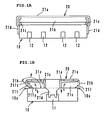
- an integrated electronic component includes a metal case 20 preferably made of phosphor bronze or white metal (nickel silver) mounted on top of a ceramic substrate 10 including a plurality of laminated ceramic sheets.
- the ceramic substrate 10 is preferably made by forming capacitor patterns, inductor patterns, and resistor patterns (none are shown) on ceramic green sheets, laminating these green sheets to define predetermined circuit elements, and then firing the green sheets.
- the incorporated circuit elements are electrically connected to each other by, for example, via holes.
- the ceramic substrate 10 has external ground electrodes 11 on its front and back surfaces and external electrodes 12 for input/output or grounding on its side surfaces. The external electrodes are connected to the incorporated circuit elements.
- the ceramic substrate 10 may have circuit elements, such as capacitors, inductors, and ICs (none are shown), on its top surface.
- the metal case 20 preferably has a substantially box-like shape, which includes a top segment 21a, side segments 21b, substrate-facing segments 21c, and terminal segments 21d.
- the top segment 21a is planar and flexible so that it can deflect by a normal external force.
- the thickness of the top segment 21c is relatively thin, preferably in the range from about 0.05 mm to about 0.15 mm, for example.
- Each of the side segments 21b has a height so that the bottom edge is not in contact with the top surface of the ceramic substrate 10 by a predetermined space therebetween.
- Each side segment 21b is disposed right above the corresponding side edge of the top surface of the ceramic substrate 10 so that each side segment 21 b is flush with each side surface of the ceramic substrate 10. This design facilitates positioning of the metal case when it is attached to the substrate.
- the terminal segments 21d are forked at the ends thereof. The end of each terminal segment 21d is soldered and is electrically and mechanically connected to the external ground electrode 11, which is positioned at the center bottom of the front or back surfaces of the ceramic substrate 10.
- the bottom edges of the substrate-facing segments 21c are in contact with the top surface of the ceramic substrate 10. Side edges of the substrate-facing segments 21c and the side segments 21b are connected at the positions opposing the comers 10a of the ceramic substrate 10. Further, predetermined spaces 21e are formed between top edges of the substrate-facing segments 21c and the top segment 21a.
- the substrate-facing segments 21 c need not be in contact with the top surface of the ceramic substrate 10. Instead, the substrate-facing segments 21c and the top surface of the ceramic substrate 10 may oppose each other with spaces therebetween. The spaces are preferably determined such that the bottom edges of the substrate-facing segments 21c come into contact with the ceramic substrate 10 when a normal downward external force A is applied to the metal case 20.
- the metal case 20 is preferably formed from a single metal plate, which is stamped out into a predetermined developed shape and is processed by bending.
- the substrate-facing segments 21c are bent along borders with the side segments 21b, and have the spaces 21e between their top edges and the top segment 21a. That is, the substrate-facing segments 21c are supported in a cantilevered fashion by only the borders with the side segments 21b, which are located at the positions opposing the comers 10a, and allow elastic-deformation pivoting about the borders as fulcrums in the direction of arrow b shown in Fig. 1B.
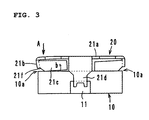
- the substrate-facing segments 21c have tapered notches 21f at the positions opposing the comers 10a of the ceramic substrate 10.
- the tapers of the notches 21 f form angles ⁇ with respect to the bottom edges of the substrate-facing segments 21 c.
- the angles ⁇ which are obtuse, basically prevent the damage of the comers 10a of the ceramic substrate 10.
- the most preferable design will be described as follows.
- the downward external force A elastically deforms the substrate-facing segments 21c as indicated by arrow b shown in Fig. 3. Accordingly, the pushing pressure on the ceramic substrate 10 is more effectively distributed.
- the optimum size of the notch 21f is determined by adjusting the angle ⁇ . That is, the range of angle ⁇ is preferably 145° ⁇ 170°. If the angle ⁇ exceeds about 170°, a tapered portion of the notches 21f easily comes into contact with the comer 10a even if deformation of the substrate-facing segments 21c, indicated by the arrow b, is small. This reduces the desirable effect. On the other hand, if the angle ⁇ is smaller than about 145°, the length of the border between the substrate-facing segment 21c and the side segment 21b is reduced, thus reducing the strength of the border portion.
- the most suitable lengths 21fx in the X direction and 21 fy in the Y direction of the notch 21 f are determined by the size of the ceramic substrate 10 under the above-described preferable range of the angle ⁇ . That is, the range of the length 21fx is preferably 0.25 mm ⁇ 21fx ⁇ 0.30 mm, for example, and the range of the length 21 fy is preferably 0.05 mm ⁇ 21fy ⁇ 0.15 mm, for example.
- the length of the ceramic substrate 10, shown in Fig. 1A preferably ranges from about 5.0 mm to about 6.5 mm, for example, and the width, shown in Fig. 1B, preferably ranges from about 4.0 mm to about 4.5 mm, for example.
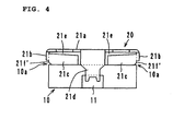
- the substrate-facing segments 21c of the metal case 20 have notches 21f' preferably having a substantially circular arc shape at the positions opposing the comers 10a of the top surface of the ceramic substrate 10.
- Other elements are identical to those in the above-described first preferred embodiment.
- the same reference numerals are used in Fig. 4 and Figs. 1 to 3 to identify the same elements and blocks, and duplicated descriptions are omitted.
- a radius of curvature R of the notches 21f' is preferably about 0.05 mm to about 0.2 mm, for example, about 0.1 mm. If the radius of curvature R is smaller than about 0.05 mm, the substantially circular arc portion of the notches 21f' easily comes into contact with the comer 10a even if the deformation of the substrate-facing segments 21c is small. This reduces the desirable effect. On the other hand, a radius of curvature R exceeding about 0.2 mm reduces the length of the border between the substrate-facing segment 21c and the side segment 21b, and thus reduces the strength of the border portion.
- the notches 21 f instead of the notches 21 f having a linear shape, the notches 21f' having a substantially circular arc shape are formed.
- the stress normally concentrated on the comers 10a of the top surface of the ceramic substrate 10 is more smoothly distributed.
- the substrate-facing segments 21c are elastically deformed by the external force as in the first preferred embodiment.
- the structure of the ceramic substrate and the detailed shape of the metal case can be determined freely.
- the terminal segments 21d are soldered to the external electrodes 11 in the above-described preferred embodiments, a method for securing the metal case and the ceramic substrate can be determined freely.
- various types of circuit elements, which are incorporated in the ceramic substrate or mounted on the ceramic substrate, can be used.
Landscapes
- Engineering & Computer Science (AREA)
- Microelectronics & Electronic Packaging (AREA)
- Structure Of Printed Boards (AREA)
- Casings For Electric Apparatus (AREA)
Abstract

Description
Claims (19)
- An integrated electronic component comprising:wherein bottom edges of the substrate-facing segments oppose a top surface of the ceramic substrate, the substrate-facing segments have notches at positions opposing comers of the top surface of the ceramic substrate, and the notches have a tapered shape having obtuse angles with respect to the bottom edges of the substrate-facing segments.a ceramic substrate including circuit elements; anda metal case having a top segment and substrate-facing segments and being mounted on the ceramic substrate;
- An integrated electronic component according to Claim 1, wherein the metal case includes side segments, the substrate-facing segments are seamlessly connected to the side segments at positions opposing the comers of the top surface of the ceramic substrate, and the substrate-facing segments are separated from the top surface, thereby the substrate-facing segments being supported at borders with the side segments in a cantilevered fashion.
- An integrated electronic component according to Claim 1, wherein the circuit elements are disposed within the ceramic substrate.
- An integrated electronic component according to Claim 1, wherein the circuit elements are mounted on the ceramic substrate.
- An integrated electronic component according to Claim 1, wherein the metal case is of at least one of phosphor bronze and nickel silver.
- An integrated electronic component according to Claim 1, wherein the ceramic substrate includes a plurality of laminated ceramic sheets.
- An integrated electronic component according to Claim 1, wherein the metal case has a substantially box-like shape.
- An integrated electronic component according to Claim 1, wherein the obtuse angles are within the range of 145°≤≤170°.
- An integrated electronic component according to Claim 1, wherein each of the notches has a length in a first direction that is within the range of about 0.25 mm to about 0.30 mm and a length in a second direction that is within the range of about 0.05 mm to about 0.15 mm.
- An integrated electronic component according to Claim 1, wherein the ceramic substrate has a length of about 5.0 mm to about 6.5 mm, and has a width of about 4.0 mm to about 4.5 mm.
- An integrated electronic component comprising:wherein bottom edges of the substrate-facing segments oppose a top surface of the ceramic substrate, the substrate-facing segments have notches at positions opposing comers of the top surface of the ceramic substrate, and the notches have a substantially circular arc shape.a ceramic substrate including circuit elements; anda metal case having a top segment and substrate-facing segments and being mounted on the ceramic substrate;
- An integrated electronic component according to Claim 11, wherein the metal case includes side segments, the substrate-facing segments are seamlessly connected to the side segments at positions opposing the comers of the top surface of the ceramic substrate, and the substrate-facing segments are separated from the top surface, thereby the substrate-facing segments being supported at borders with the side segments in a cantilevered fashion.
- An integrated electronic component according to Claim 11, wherein the circuit elements are disposed within the ceramic substrate.
- An integrated electronic component according to Claim 11, wherein the circuit elements are mounted on the ceramic substrate.
- An integrated electronic component according to Claim 11, wherein the metal case is of at least one of phosphor bronze and nickel silver.
- An integrated electronic component according to Claim 11, wherein the ceramic substrate includes a plurality of laminated ceramic sheets.
- An integrated electronic component according to Claim 11, wherein the metal case has a substantially box-like shape.
- An integrated electronic component according to Claim 1, wherein a radius of curvature R of the notches is about 0.05 mm to about 0.2 mm.
- An integrated electronic component according to Claim 11, wherein the ceramic substrate has a length of about 5.0 mm to about 6.5 mm, and has a width of about 4.0 mm to about 4.5 mm.
Applications Claiming Priority (2)
| Application Number | Priority Date | Filing Date | Title |
|---|---|---|---|
| JP2003146550 | 2003-05-23 | ||
| JP2003146550A JP4107160B2 (en) | 2003-05-23 | 2003-05-23 | Composite electronic components |
Publications (3)
| Publication Number | Publication Date |
|---|---|
| EP1480267A2 true EP1480267A2 (en) | 2004-11-24 |
| EP1480267A3 EP1480267A3 (en) | 2008-07-09 |
| EP1480267B1 EP1480267B1 (en) | 2012-01-11 |
Family
ID=33095494
Family Applications (1)
| Application Number | Title | Priority Date | Filing Date |
|---|---|---|---|
| EP04003767A Expired - Lifetime EP1480267B1 (en) | 2003-05-23 | 2004-02-19 | Integrated electronic component |
Country Status (5)
| Country | Link |
|---|---|
| US (1) | US7126057B2 (en) |
| EP (1) | EP1480267B1 (en) |
| JP (1) | JP4107160B2 (en) |
| CN (1) | CN100466121C (en) |
| AT (1) | ATE541311T1 (en) |
Families Citing this family (6)
| Publication number | Priority date | Publication date | Assignee | Title |
|---|---|---|---|---|
| JP4301071B2 (en) * | 2004-05-07 | 2009-07-22 | 株式会社村田製作所 | Electronic component with shield case and method of manufacturing the same |
| DE102005004158B4 (en) * | 2005-01-28 | 2006-11-30 | Siemens Ag | Arrangement for shielding base boards with a shroud |
| US8336200B2 (en) * | 2006-05-26 | 2012-12-25 | Sg Design Technologies | Apparatus, system, and method for maintaining part orientation during manufacturing |
| US7875228B2 (en) * | 2006-05-26 | 2011-01-25 | Sg Design Technologies | Apparatus, system, and method for maintaining part orientation during manufacturing |
| JP4020149B1 (en) * | 2006-06-19 | 2007-12-12 | 株式会社村田製作所 | Electronic component module |
| JP2020155517A (en) * | 2019-03-19 | 2020-09-24 | キオクシア株式会社 | Semiconductor device |
Family Cites Families (7)
| Publication number | Priority date | Publication date | Assignee | Title |
|---|---|---|---|---|
| JPH0411349Y2 (en) * | 1985-12-03 | 1992-03-19 | ||
| JP2850860B2 (en) * | 1996-06-24 | 1999-01-27 | 住友金属工業株式会社 | Electronic component manufacturing method |
| JPH10284935A (en) * | 1997-04-09 | 1998-10-23 | Murata Mfg Co Ltd | Voltage controlled oscillator and method of manufacturing the same |
| JP3714088B2 (en) * | 1999-02-18 | 2005-11-09 | 株式会社村田製作所 | Electronic component and manufacturing method thereof |
| JP2001148594A (en) * | 1999-11-19 | 2001-05-29 | Murata Mfg Co Ltd | Electronic device with shield case |
| JP3698305B2 (en) * | 2000-09-07 | 2005-09-21 | シャープ株式会社 | High frequency module and manufacturing method thereof |
| JP3736387B2 (en) * | 2001-05-25 | 2006-01-18 | 株式会社村田製作所 | Composite electronic component and manufacturing method thereof |
-
2003
- 2003-05-23 JP JP2003146550A patent/JP4107160B2/en not_active Expired - Lifetime
-
2004
- 2004-02-10 US US10/774,440 patent/US7126057B2/en not_active Expired - Lifetime
- 2004-02-19 AT AT04003767T patent/ATE541311T1/en active
- 2004-02-19 EP EP04003767A patent/EP1480267B1/en not_active Expired - Lifetime
- 2004-05-24 CN CNB2004100474790A patent/CN100466121C/en not_active Expired - Lifetime
Also Published As
| Publication number | Publication date |
|---|---|
| CN100466121C (en) | 2009-03-04 |
| JP4107160B2 (en) | 2008-06-25 |
| US20040233647A1 (en) | 2004-11-25 |
| ATE541311T1 (en) | 2012-01-15 |
| CN1574131A (en) | 2005-02-02 |
| US7126057B2 (en) | 2006-10-24 |
| EP1480267A3 (en) | 2008-07-09 |
| EP1480267B1 (en) | 2012-01-11 |
| JP2004349559A (en) | 2004-12-09 |
Similar Documents
| Publication | Publication Date | Title |
|---|---|---|
| US7989045B2 (en) | Elastic sheet structure and array type elastic sheet device using the same | |
| US11895769B2 (en) | Module, terminal assembly, and method for producing module | |
| EP1030323A1 (en) | Ceramic electronic component | |
| EP1050906A1 (en) | Package for electronic components | |
| CN1118203A (en) | double arm contact | |
| EP1473802B1 (en) | Tab terminal | |
| JP6939982B2 (en) | High frequency module | |
| US7126057B2 (en) | Integrated electronic component | |
| US20090176397A1 (en) | Electrical connector having improved load plate | |
| EP1143577B1 (en) | Conductive element and manufacturing method thereof | |
| US5844468A (en) | Chip network electronic component | |
| WO2001022788A1 (en) | Double sided gasket | |
| JP3453631B2 (en) | Connector and its manufacturing and mounting method | |
| JPH09186042A (en) | Laminated electronic component | |
| US20030169583A1 (en) | Shielding structure suitable for use with transmitter-receivers | |
| US5721044A (en) | Multiple substrate | |
| JP2004254251A (en) | Surface mount type piezoelectric vibrator and insulating package | |
| JP4787718B2 (en) | Tab terminal | |
| JP2003257520A (en) | Push-type board connector | |
| JPH113696A (en) | Battery terminals | |
| JPH06310862A (en) | Ceramic multilayered circuit board with cavity | |
| JP2003086969A (en) | Terminal structure of electronic components | |
| JPH05299294A (en) | Manufacture of electronic component | |
| JPH09199242A (en) | Printed wiring board integrated connector and manufacturing method thereof | |
| JP3221350B2 (en) | Multilayer chip components |
Legal Events
| Date | Code | Title | Description |
|---|---|---|---|
| PUAI | Public reference made under article 153(3) epc to a published international application that has entered the european phase |
Free format text: ORIGINAL CODE: 0009012 |
|
| 17P | Request for examination filed |
Effective date: 20040219 |
|
| AK | Designated contracting states |
Kind code of ref document: A2 Designated state(s): AT BE BG CH CY CZ DE DK EE ES FI FR GB GR HU IE IT LI LU MC NL PT RO SE SI SK TR |
|
| AX | Request for extension of the european patent |
Extension state: AL LT LV MK |
|
| RAP1 | Party data changed (applicant data changed or rights of an application transferred) |
Owner name: MURATA MANUFACTURING CO., LTD. |
|
| PUAL | Search report despatched |
Free format text: ORIGINAL CODE: 0009013 |
|
| AK | Designated contracting states |
Kind code of ref document: A3 Designated state(s): AT BE BG CH CY CZ DE DK EE ES FI FR GB GR HU IE IT LI LU MC NL PT RO SE SI SK TR |
|
| AX | Request for extension of the european patent |
Extension state: AL LT LV MK |
|
| AKX | Designation fees paid |
Designated state(s): AT BE BG CH CY CZ DE DK EE ES FI FR GB GR HU IE IT LI LU MC NL PT RO SE SI SK TR |
|
| 17Q | First examination report despatched |
Effective date: 20101015 |
|
| GRAP | Despatch of communication of intention to grant a patent |
Free format text: ORIGINAL CODE: EPIDOSNIGR1 |
|
| GRAS | Grant fee paid |
Free format text: ORIGINAL CODE: EPIDOSNIGR3 |
|
| GRAA | (expected) grant |
Free format text: ORIGINAL CODE: 0009210 |
|
| AK | Designated contracting states |
Kind code of ref document: B1 Designated state(s): AT BE BG CH CY CZ DE DK EE ES FI FR GB GR HU IE IT LI LU MC NL PT RO SE SI SK TR |
|
| REG | Reference to a national code |
Ref country code: GB Ref legal event code: FG4D |
|
| REG | Reference to a national code |
Ref country code: CH Ref legal event code: EP |
|
| REG | Reference to a national code |
Ref country code: AT Ref legal event code: REF Ref document number: 541311 Country of ref document: AT Kind code of ref document: T Effective date: 20120115 |
|
| REG | Reference to a national code |
Ref country code: IE Ref legal event code: FG4D |
|
| REG | Reference to a national code |
Ref country code: DE Ref legal event code: R096 Ref document number: 602004036043 Country of ref document: DE Effective date: 20120308 |
|
| REG | Reference to a national code |
Ref country code: NL Ref legal event code: VDEP Effective date: 20120111 |
|
| PG25 | Lapsed in a contracting state [announced via postgrant information from national office to epo] |
Ref country code: SI Free format text: LAPSE BECAUSE OF FAILURE TO SUBMIT A TRANSLATION OF THE DESCRIPTION OR TO PAY THE FEE WITHIN THE PRESCRIBED TIME-LIMIT Effective date: 20120111 |
|
| PG25 | Lapsed in a contracting state [announced via postgrant information from national office to epo] |
Ref country code: BE Free format text: LAPSE BECAUSE OF FAILURE TO SUBMIT A TRANSLATION OF THE DESCRIPTION OR TO PAY THE FEE WITHIN THE PRESCRIBED TIME-LIMIT Effective date: 20120111 Ref country code: NL Free format text: LAPSE BECAUSE OF FAILURE TO SUBMIT A TRANSLATION OF THE DESCRIPTION OR TO PAY THE FEE WITHIN THE PRESCRIBED TIME-LIMIT Effective date: 20120111 Ref country code: BG Free format text: LAPSE BECAUSE OF FAILURE TO SUBMIT A TRANSLATION OF THE DESCRIPTION OR TO PAY THE FEE WITHIN THE PRESCRIBED TIME-LIMIT Effective date: 20120411 |
|
| PG25 | Lapsed in a contracting state [announced via postgrant information from national office to epo] |
Ref country code: FI Free format text: LAPSE BECAUSE OF FAILURE TO SUBMIT A TRANSLATION OF THE DESCRIPTION OR TO PAY THE FEE WITHIN THE PRESCRIBED TIME-LIMIT Effective date: 20120111 Ref country code: PT Free format text: LAPSE BECAUSE OF FAILURE TO SUBMIT A TRANSLATION OF THE DESCRIPTION OR TO PAY THE FEE WITHIN THE PRESCRIBED TIME-LIMIT Effective date: 20120511 Ref country code: GR Free format text: LAPSE BECAUSE OF FAILURE TO SUBMIT A TRANSLATION OF THE DESCRIPTION OR TO PAY THE FEE WITHIN THE PRESCRIBED TIME-LIMIT Effective date: 20120412 |
|
| REG | Reference to a national code |
Ref country code: AT Ref legal event code: MK05 Ref document number: 541311 Country of ref document: AT Kind code of ref document: T Effective date: 20120111 |
|
| PG25 | Lapsed in a contracting state [announced via postgrant information from national office to epo] |
Ref country code: CY Free format text: LAPSE BECAUSE OF FAILURE TO SUBMIT A TRANSLATION OF THE DESCRIPTION OR TO PAY THE FEE WITHIN THE PRESCRIBED TIME-LIMIT Effective date: 20120111 Ref country code: MC Free format text: LAPSE BECAUSE OF NON-PAYMENT OF DUE FEES Effective date: 20120229 |
|
| REG | Reference to a national code |
Ref country code: CH Ref legal event code: PL |
|
| PG25 | Lapsed in a contracting state [announced via postgrant information from national office to epo] |
Ref country code: CZ Free format text: LAPSE BECAUSE OF FAILURE TO SUBMIT A TRANSLATION OF THE DESCRIPTION OR TO PAY THE FEE WITHIN THE PRESCRIBED TIME-LIMIT Effective date: 20120111 Ref country code: RO Free format text: LAPSE BECAUSE OF FAILURE TO SUBMIT A TRANSLATION OF THE DESCRIPTION OR TO PAY THE FEE WITHIN THE PRESCRIBED TIME-LIMIT Effective date: 20120111 Ref country code: DK Free format text: LAPSE BECAUSE OF FAILURE TO SUBMIT A TRANSLATION OF THE DESCRIPTION OR TO PAY THE FEE WITHIN THE PRESCRIBED TIME-LIMIT Effective date: 20120111 Ref country code: SE Free format text: LAPSE BECAUSE OF FAILURE TO SUBMIT A TRANSLATION OF THE DESCRIPTION OR TO PAY THE FEE WITHIN THE PRESCRIBED TIME-LIMIT Effective date: 20120111 Ref country code: CH Free format text: LAPSE BECAUSE OF NON-PAYMENT OF DUE FEES Effective date: 20120229 Ref country code: EE Free format text: LAPSE BECAUSE OF FAILURE TO SUBMIT A TRANSLATION OF THE DESCRIPTION OR TO PAY THE FEE WITHIN THE PRESCRIBED TIME-LIMIT Effective date: 20120111 Ref country code: LI Free format text: LAPSE BECAUSE OF NON-PAYMENT OF DUE FEES Effective date: 20120229 |
|
| PLBE | No opposition filed within time limit |
Free format text: ORIGINAL CODE: 0009261 |
|
| STAA | Information on the status of an ep patent application or granted ep patent |
Free format text: STATUS: NO OPPOSITION FILED WITHIN TIME LIMIT |
|
| REG | Reference to a national code |
Ref country code: IE Ref legal event code: MM4A |
|
| REG | Reference to a national code |
Ref country code: FR Ref legal event code: ST Effective date: 20121031 |
|
| PG25 | Lapsed in a contracting state [announced via postgrant information from national office to epo] |
Ref country code: IT Free format text: LAPSE BECAUSE OF FAILURE TO SUBMIT A TRANSLATION OF THE DESCRIPTION OR TO PAY THE FEE WITHIN THE PRESCRIBED TIME-LIMIT Effective date: 20120111 Ref country code: SK Free format text: LAPSE BECAUSE OF FAILURE TO SUBMIT A TRANSLATION OF THE DESCRIPTION OR TO PAY THE FEE WITHIN THE PRESCRIBED TIME-LIMIT Effective date: 20120111 |
|
| 26N | No opposition filed |
Effective date: 20121012 |
|
| GBPC | Gb: european patent ceased through non-payment of renewal fee |
Effective date: 20120411 |
|
| PG25 | Lapsed in a contracting state [announced via postgrant information from national office to epo] |
Ref country code: IE Free format text: LAPSE BECAUSE OF NON-PAYMENT OF DUE FEES Effective date: 20120219 Ref country code: GB Free format text: LAPSE BECAUSE OF NON-PAYMENT OF DUE FEES Effective date: 20120411 Ref country code: AT Free format text: LAPSE BECAUSE OF FAILURE TO SUBMIT A TRANSLATION OF THE DESCRIPTION OR TO PAY THE FEE WITHIN THE PRESCRIBED TIME-LIMIT Effective date: 20120111 Ref country code: FR Free format text: LAPSE BECAUSE OF NON-PAYMENT OF DUE FEES Effective date: 20120312 |
|
| REG | Reference to a national code |
Ref country code: DE Ref legal event code: R097 Ref document number: 602004036043 Country of ref document: DE Effective date: 20121012 |
|
| PG25 | Lapsed in a contracting state [announced via postgrant information from national office to epo] |
Ref country code: ES Free format text: LAPSE BECAUSE OF FAILURE TO SUBMIT A TRANSLATION OF THE DESCRIPTION OR TO PAY THE FEE WITHIN THE PRESCRIBED TIME-LIMIT Effective date: 20120422 |
|
| PG25 | Lapsed in a contracting state [announced via postgrant information from national office to epo] |
Ref country code: TR Free format text: LAPSE BECAUSE OF FAILURE TO SUBMIT A TRANSLATION OF THE DESCRIPTION OR TO PAY THE FEE WITHIN THE PRESCRIBED TIME-LIMIT Effective date: 20120111 |
|
| PG25 | Lapsed in a contracting state [announced via postgrant information from national office to epo] |
Ref country code: LU Free format text: LAPSE BECAUSE OF NON-PAYMENT OF DUE FEES Effective date: 20120219 |
|
| PG25 | Lapsed in a contracting state [announced via postgrant information from national office to epo] |
Ref country code: HU Free format text: LAPSE BECAUSE OF FAILURE TO SUBMIT A TRANSLATION OF THE DESCRIPTION OR TO PAY THE FEE WITHIN THE PRESCRIBED TIME-LIMIT Effective date: 20040219 |
|
| PGFP | Annual fee paid to national office [announced via postgrant information from national office to epo] |
Ref country code: DE Payment date: 20230216 Year of fee payment: 20 |
|
| REG | Reference to a national code |
Ref country code: DE Ref legal event code: R071 Ref document number: 602004036043 Country of ref document: DE |