JP2004349559A - Composite electronic component - Google Patents
Composite electronic component Download PDFInfo
- Publication number
- JP2004349559A JP2004349559A JP2003146550A JP2003146550A JP2004349559A JP 2004349559 A JP2004349559 A JP 2004349559A JP 2003146550 A JP2003146550 A JP 2003146550A JP 2003146550 A JP2003146550 A JP 2003146550A JP 2004349559 A JP2004349559 A JP 2004349559A
- Authority
- JP
- Japan
- Prior art keywords
- ceramic substrate
- electronic component
- facing
- composite electronic
- metal case
- Prior art date
- Legal status (The legal status is an assumption and is not a legal conclusion. Google has not performed a legal analysis and makes no representation as to the accuracy of the status listed.)
- Granted
Links
Images


Classifications
-
- H—ELECTRICITY
- H05—ELECTRIC TECHNIQUES NOT OTHERWISE PROVIDED FOR
- H05K—PRINTED CIRCUITS; CASINGS OR CONSTRUCTIONAL DETAILS OF ELECTRIC APPARATUS; MANUFACTURE OF ASSEMBLAGES OF ELECTRICAL COMPONENTS
- H05K9/00—Screening of apparatus or components against electric or magnetic fields
- H05K9/0007—Casings
- H05K9/002—Casings with localised screening
- H05K9/0022—Casings with localised screening of components mounted on printed circuit boards [PCB]
-
- H—ELECTRICITY
- H01—ELECTRIC ELEMENTS
- H01L—SEMICONDUCTOR DEVICES NOT COVERED BY CLASS H10
- H01L23/00—Details of semiconductor or other solid state devices
- H01L23/02—Containers; Seals
- H01L23/04—Containers; Seals characterised by the shape of the container or parts, e.g. caps, walls
-
- H—ELECTRICITY
- H01—ELECTRIC ELEMENTS
- H01L—SEMICONDUCTOR DEVICES NOT COVERED BY CLASS H10
- H01L23/00—Details of semiconductor or other solid state devices
- H01L23/48—Arrangements for conducting electric current to or from the solid state body in operation, e.g. leads, terminal arrangements ; Selection of materials therefor
- H01L23/488—Arrangements for conducting electric current to or from the solid state body in operation, e.g. leads, terminal arrangements ; Selection of materials therefor consisting of soldered or bonded constructions
- H01L23/498—Leads, i.e. metallisations or lead-frames on insulating substrates, e.g. chip carriers
- H01L23/49805—Leads, i.e. metallisations or lead-frames on insulating substrates, e.g. chip carriers the leads being also applied on the sidewalls or the bottom of the substrate, e.g. leadless packages for surface mounting
-
- H—ELECTRICITY
- H01—ELECTRIC ELEMENTS
- H01L—SEMICONDUCTOR DEVICES NOT COVERED BY CLASS H10
- H01L2924/00—Indexing scheme for arrangements or methods for connecting or disconnecting semiconductor or solid-state bodies as covered by H01L24/00
- H01L2924/0001—Technical content checked by a classifier
- H01L2924/0002—Not covered by any one of groups H01L24/00, H01L24/00 and H01L2224/00
Landscapes
- Engineering & Computer Science (AREA)
- Microelectronics & Electronic Packaging (AREA)
- Physics & Mathematics (AREA)
- Condensed Matter Physics & Semiconductors (AREA)
- General Physics & Mathematics (AREA)
- Computer Hardware Design (AREA)
- Power Engineering (AREA)
- Structure Of Printed Boards (AREA)
- Casings For Electric Apparatus (AREA)
Abstract
Description
【0001】
【発明の属する技術分野】
本発明は、複合電子部品、特に、回路素子を内蔵及び/又は搭載したセラミック基板に金属ケースを取り付けた複合電子部品に関する。
【0002】
【従来の技術と課題】
【特許文献1】
特開2002−353071号公報
【0003】
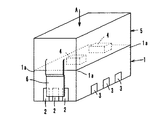
従来、コンデンサやインダクタ等の回路素子を内蔵及び/又は搭載した複合電子部品として、特許文献1に記載のものが知られている。この種の複合電子部品は、図5に示すように、多数枚のセラミックシートを積層してなる基板1の上面に金属ケース5が取り付けられている。
【0004】
セラミック基板1は、その内部に図示しない回路素子を内蔵し、さらに、その上面には回路素子4が搭載され、端面及び側面には外部電極2,3が設けられている。金属ケース5は、略箱形状をなし、セラミック基板1の上面に載置され、両端部に突設した端子部6が外部電極2とはんだ付けされ電気的に接続されている。
【0005】
ところで、この種の複合電子部品では、金属ケース5に対して上方から外力Aが作用する場合が多い。例えば、セラミック基板1に金属ケースを組み付ける際、完成品の電気的特性を測定する際や、完成品を配線基板に実装する際などに、吸着治具が金属ケース5の上面を下方へ押圧するからである。このように外力Aが作用すると、金属ケース5の下縁部がセラミック基板1の上面を押圧し、これにてセラミック基板の上面の角部1aに欠けやクラックが発生しやすいという問題点を有していた。
【0006】
前記外力Aに起因する応力は上面角部1aに集中する傾向にあり、かつ、上面角部1aはセラミック基板1の最も脆弱な部分でもあり、損傷しやすい。
【0007】
そこで、本発明の目的は、金属ケースに作用する外力によってセラミック基板が損傷することを防止した複合電子部品を提供することにある。
【0008】
【課題を解決するための手段及び作用】
以上の目的を達成するため、第1の発明は、回路素子を内蔵及び/又は搭載したセラミック基板に、少なくとも上面部及び対向部を有する金属ケースを取り付けた複合電子部品において、前記対向部はその下端が前記セラミック基板の上面と対向するとともに、該セラミック基板の上面角部と対向する部分に、下端と鈍角をなすテーパ状の切欠き部が形成されていることを特徴とする。
【0009】
また、第2の発明は、回路素子を内蔵及び/又は搭載したセラミック基板に、少なくとも上面部及び対向部を有する金属ケースを取り付けた複合電子部品において、前記対向部はその下端が前記セラミック基板の上面と対向するとともに、該セラミック基板の上面角部と対向する部分に、円弧状をなす切欠き部が形成されていることを特徴とする。
【0010】
第1の発明にあっては、金属ケースの対向部がセラミック基板の上面角部と対向する部分に、下端と鈍角をなすテーパ状の切欠き部が形成されているため、また、第2の発明にあっては、円弧状をなす切欠き部が形成されているため、金属ケースに上方から外力が作用したとしても、前記切欠き部がセラミック基板の上面角部に加わる押圧力を逃がすことができる。よって、応力が集中しやすく、脆弱な部分でもあるセラミック基板の上面角部に欠けやクラックなどの損傷が発生することが未然に防止される。
【0011】
特に、前記第1及び第2の発明にあっては、金属ケースの対向部が、セラミック基板の上面角部と対向する部分で金属ケースの側面部と繋がっており、かつ、対向部と上面部とは隙間を有し、上面角部で片持ち支持されていることが好ましい。対向部が前記隙間により弾性変形可能となり、金属ケースに外力が作用した際に、セラミック基板に加わる押圧力をより効果的に逃がすことが可能となる。
【0012】
【発明の実施の形態】
以下、本発明に係る複合電子部品の実施形態について、添付図面を参照して説明する。
【0013】
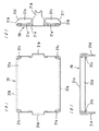
(第1実施形態、図1〜図3参照)
第1実施形態としての複合電子部品は、図1に示すように、多数枚のセラミックシートを積層してなるセラミック基板10の上面に、リン青銅あるいは洋白(ニッケルシルバー)等からなる金属ケース20を取り付けたものである。
【0014】
セラミック基板10は、セラミックグリーンシート上に図示しないコンデンサパターン、インダクタパターン、抵抗体パターンなどを形成し、これらのシートを積層して所定の回路素子を構成し、その後に焼成したもので、内蔵された回路素子はビアホールなどによって電気的に接続されている。また、セラミック基板10の端面及び側面には内蔵回路素子と接続されているグランド用外部電極11と、入出力用外部電極またはグランド用外部電極12が形成されている。
【0015】
なお、セラミック基板10は、その上面にも図示しないがコンデンサやインダクタやICなどの回路素子が搭載されていてもよい。
【0016】
金属ケース20は、図2に示すように、上面部21a、側面部21b、対向部21c、端子部21dからなる略箱形状を有している。上面部21aは平坦状であり、通常金属ケースに加わる外力により撓むような強度を有している。金属ケースの厚みとしては0.05〜0.15mmといった比較的薄いものを用いている。
【0017】
側面部21bはその下端がセラミック基板10の上面とは当接しないように所定の間隔を有して形成されている。また、側面部21bはセラミック基板10の上面縁部のほぼ真上に設けられることにより、セラミック基板の側面とは面一となっている。このように面一とする方が金属ケースを取り付けるときに位置決めが容易である。端子部21dは、先端が2つに分かれているとともに、その先端がセラミック基板10の端面中央部下端に形成されたグランド用外部電極11にはんだ付けされることにより、電気的に接続されかつ機械的に固定されている。
【0018】
対向部21cは、その下端がセラミック基板10の上面と当接している。また、対向部21cと側面部21bはセラミック基板10の上面角部10aに対向する部分で繋がっている。さらに、対向部21cの上端と上面部21aとは所定の隙間21eを有する構造となっている。なお、対向部21cはセラミック基板10の上面と当接していなくてもよく、隙間を有して対向していればよい。隙間を空ける場合には、金属ケース20に上方から外力Aが作用したときに、対向部21cの下端がセラミック基板10に当接するような隙間に設定することが好ましい。
【0019】
金属ケース20は1枚の金属板を所定の展開形状に打ち抜き、折曲げ加工を施したものである。対向部21cは側面部21bとの連続部分で折り曲げられ、上面部21aとは隙間21eを有している。即ち、対向部21cは側面部21bとの連続部分(上面角部10aに対向する部分)で片持ち支持され、該連続部分を支点として矢印b方向(図1(B)参照)に弾性変形可能である。
【0020】
さらに、対向部21cにはセラミック基板10の上面角部10aと対向する部分に、対向部21cの下端と角度θをなすテーパ状の切欠き部21fが形成されている。この角度θは基本的には鈍角であれば本願の作用効果を奏するものであるが、最適な条件については後述する。
【0021】
以上の構成からなる複合電子部品においては、図3に示すように、金属ケース20に上方から外力Aが作用した場合、対向部21cからセラミック基板10の上面角部10aに押圧力が集中することになるが、その集中部分には切欠き部21fが形成されているため、押圧力が拡散され、セラミック基板10の上面角部10aに応力が集中することが回避され、比較的脆弱な上面角部10aに欠けやクラックなどの損傷が発生することはない。
【0022】
特に、対向部21cが側面部21bとの連続部分で片持ち支持されていることにより、外力Aの作用で対向部21cが図3に矢印bで示すように弾性的に変形するので、セラミック基板10に加わる押圧力がより効果的に拡散される。
【0023】
ここで、切欠き部21fについて詳述する。切欠き部21fは角度θを調整することにより最適な大きさに設定される。すなわち、角度θは145゜≦θ≦170゜に設定することが好ましい。角度θが170゜よりも大きい場合には、矢印bで示す対向部21cの変形が小さくても、切欠き部21fのテーパ部分が上面角部10aにすぐに当接してしまい、効果的でない。一方、145゜より小さい場合には、対向部21cと側面部21bとの連続部分の幅が細くなってしまい、連続部分の強度が低下する。
【0024】
また、x方向の寸法(21fx)及びy方向の寸法(21fy)においても、前記θの条件を満たしつつ、セラミック基板10の大きさに合わせて最適な大きさが設定される。すなわち、21fxは0.25mm≦21fx≦0.30mm、21fyは0.05mm≦21fy≦0.15mmの範囲に設定することが好ましい。なお、セラミック基板10の寸法は、図1(A)に示す長手方向が5.0〜6.5mm、図1(B)に示す幅方向が4.0〜4.5mmである。
【0025】
(第2実施形態、図4参照)
第2実施形態としての複合電子部品は、図4に示すように、金属ケース20の対向部21cであってセラミック基板10の上面角部10aと対向する部分に、円弧状をなす切欠き部21f’を形成したものである。他の構成は、前記第1実施形態と同様であり、図4において図1〜図3と同じ部分には同じ符号を付し、重複する説明は省略する。
【0026】
ここで、切欠き部21f’の曲率Rは0.05〜0.2mm(例えば0.1mm)である。曲率Rが0.05mmより小さい場合には、対向部21cの変形が小さくても、切欠き部21f’のR部分が上面角部10aにすぐに当接してしまい、効果的でない。一方、曲率Rが0.2mmより大きい場合には、対向部21cと側面部21bとの連続部分の幅が細くなってしまい、連続部分の強度が低下する。
【0027】
本第2実施形態は、前記第1実施形態で示した直線状の切欠き部21fに代えて円弧状の切欠き部21f’を形成したもので、金属ケース10に上方から外力が作用した場合、セラミック基板10の上面角部10aに集中する応力をよりスムーズに逃がすことができる。また、対向部21cが外力の作用で弾性変形することも前記第1実施形態と同様である。
【0028】
(他の実施形態)
なお、本発明に係る複合電子部品は前記実施形態に限定するものではなく、その要旨の範囲内で種々に変更できる。
【0029】
特に、セラミック基板の構成や金属ケースの詳細な形状は任意であり、金属ケースとセラミック基板との固定方法(前記実施形態では端子部21dを外部電極11にはんだ付けしている)も任意である。また、セラミック基板に内蔵あるいは搭載される回路素子は種々のものが存在する。
【0030】
【発明の効果】
以上の説明で明らかなように、本発明によれば、金属ケースに上方から外力が作用したとしても、金属ケースの対向部に形成した切欠き部によってセラミック基板の上面角部に応力が集中することが防止され、比較的脆弱な上面角部の損傷を効果的に防止することができる。
【図面の簡単な説明】
【図1】本発明に係る複合電子部品の第1実施形態を示し、(A)は正面図、(B)は側面図である。
【図2】前記第1実施形態の金属ケースを示し、(A)は平面図、(B)は正面図、(C)は側面図である。
【図3】前記第1実施形態において金属ケースに外力が作用した状態を示す側面図である。
【図4】本発明に係る複合電子部品の第2実施形態を示す側面図である。
【図5】従来の複合電子部品を示す斜視図である。
【符号の説明】
10…セラミック基板
10a…上面角部
20…金属ケース
21b…側面部
21c…対向部
21f,21f’…切欠き部[0001]
TECHNICAL FIELD OF THE INVENTION
The present invention relates to a composite electronic component, and more particularly to a composite electronic component in which a metal case is attached to a ceramic substrate having a built-in and / or mounted circuit element.
[0002]
[Prior art and problems]
[Patent Document 1]
JP-A-2002-353071
DESCRIPTION OF RELATED ART Conventionally, the thing of
[0004]
The
[0005]
By the way, in this type of composite electronic component, an external force A acts on the
[0006]
The stress caused by the external force A tends to concentrate on the upper corner 1a, and the upper corner 1a is also the weakest part of the
[0007]
Accordingly, an object of the present invention is to provide a composite electronic component in which a ceramic substrate is prevented from being damaged by an external force acting on a metal case.
[0008]
Means and Action for Solving the Problems
In order to achieve the above object, a first invention is a composite electronic component in which a metal case having at least an upper surface portion and a facing portion is attached to a ceramic substrate on which a circuit element is built and / or mounted, wherein the facing portion is A lower end is opposed to the upper surface of the ceramic substrate, and a tapered notch is formed at a portion opposed to a corner of the upper surface of the ceramic substrate so as to form an obtuse angle with the lower end.
[0009]
According to a second aspect of the present invention, in a composite electronic component in which a metal case having at least an upper surface portion and a facing portion is attached to a ceramic substrate having a built-in and / or mounted circuit element, the lower end of the facing portion has a lower surface than the ceramic substrate. An arc-shaped notch is formed in a portion facing the upper surface and facing a corner of the upper surface of the ceramic substrate.
[0010]
According to the first invention, a tapered notch that forms an obtuse angle with the lower end is formed in a portion where the facing portion of the metal case faces the upper corner of the ceramic substrate. According to the present invention, since the notch having an arc shape is formed, even if an external force acts on the metal case from above, the notch releases the pressing force applied to the upper surface corner of the ceramic substrate. Can be. Therefore, damage such as chipping or cracking is prevented from occurring at the corners of the upper surface of the ceramic substrate, which are fragile portions where stress is easily concentrated.
[0011]
In particular, in the first and second inventions, the facing portion of the metal case is connected to the side portion of the metal case at a portion facing the upper corner portion of the ceramic substrate, and the facing portion and the upper surface portion are connected to each other. It is preferable that there is a gap and the cantilever is supported at the corner of the upper surface. The facing portion can be elastically deformed by the gap, so that when an external force acts on the metal case, the pressing force applied to the ceramic substrate can be released more effectively.
[0012]
BEST MODE FOR CARRYING OUT THE INVENTION
Hereinafter, embodiments of a composite electronic component according to the present invention will be described with reference to the accompanying drawings.
[0013]
(1st Embodiment, FIGS. 1-3)
As shown in FIG. 1, the composite electronic component according to the first embodiment has a
[0014]
The
[0015]
Although not shown, the
[0016]
As shown in FIG. 2, the
[0017]
The
[0018]
The lower end of the facing
[0019]
The
[0020]
Further, a
[0021]
In the composite electronic component having the above configuration, as shown in FIG. 3, when an external force A acts on the
[0022]
In particular, since the facing
[0023]
Here, the
[0024]
Also, the dimensions in the x-direction (21fx) and the dimensions in the y-direction (21fy) are set to optimal sizes in accordance with the size of the
[0025]
(Second embodiment, see FIG. 4)
As shown in FIG. 4, the composite electronic component according to the second embodiment has an arc-shaped
[0026]
Here, the curvature R of the
[0027]
In the second embodiment, an arc-shaped
[0028]
(Other embodiments)
The composite electronic component according to the present invention is not limited to the above-described embodiment, but can be variously modified within the scope of the gist.
[0029]
In particular, the configuration of the ceramic substrate and the detailed shape of the metal case are arbitrary, and the method of fixing the metal case and the ceramic substrate (in the above-described embodiment, the
[0030]
【The invention's effect】
As apparent from the above description, according to the present invention, even when an external force acts on the metal case from above, the stress concentrates on the upper surface corner of the ceramic substrate due to the notch formed in the facing portion of the metal case. Is prevented, and damage to the relatively fragile upper corner can be effectively prevented.
[Brief description of the drawings]
1A and 1B show a first embodiment of a composite electronic component according to the present invention, wherein FIG. 1A is a front view and FIG. 1B is a side view.
2A and 2B show a metal case of the first embodiment, wherein FIG. 2A is a plan view, FIG. 2B is a front view, and FIG. 2C is a side view.
FIG. 3 is a side view showing a state where an external force acts on a metal case in the first embodiment.
FIG. 4 is a side view showing a second embodiment of the composite electronic component according to the present invention.
FIG. 5 is a perspective view showing a conventional composite electronic component.
[Explanation of symbols]
10
Claims (3)
前記対向部はその下端が前記セラミック基板の上面と対向するとともに、該セラミック基板の上面角部と対向する部分に、下端と鈍角をなすテーパ状の切欠き部が形成されていること、
を特徴とする複合電子部品。In a composite electronic component in which a metal case having at least an upper surface portion and a facing portion is attached to a ceramic substrate on which a circuit element is built and / or mounted,
The opposing portion has a lower end facing the upper surface of the ceramic substrate, and a portion facing the upper surface corner of the ceramic substrate is formed with a tapered notch forming an obtuse angle with the lower end,
A composite electronic component characterized by the following.
前記対向部はその下端が前記セラミック基板の上面と対向するとともに、該セラミック基板の上面角部と対向する部分に、円弧状をなす切欠き部が形成されていること、
を特徴とする複合電子部品。In a composite electronic component in which a metal case having at least an upper surface portion and a facing portion is attached to a ceramic substrate on which a circuit element is built and / or mounted,
The opposed portion has a lower end facing the upper surface of the ceramic substrate, and a portion facing the upper surface corner of the ceramic substrate is formed with an arc-shaped notch,
A composite electronic component characterized by the following.
Priority Applications (5)
| Application Number | Priority Date | Filing Date | Title |
|---|---|---|---|
| JP2003146550A JP4107160B2 (en) | 2003-05-23 | 2003-05-23 | Composite electronic components |
| US10/774,440 US7126057B2 (en) | 2003-05-23 | 2004-02-10 | Integrated electronic component |
| EP04003767A EP1480267B1 (en) | 2003-05-23 | 2004-02-19 | Integrated electronic component |
| AT04003767T ATE541311T1 (en) | 2003-05-23 | 2004-02-19 | INTEGRATED ELECTRONIC COMPONENT |
| CNB2004100474790A CN100466121C (en) | 2003-05-23 | 2004-05-24 | Integrated electronic component |
Applications Claiming Priority (1)
| Application Number | Priority Date | Filing Date | Title |
|---|---|---|---|
| JP2003146550A JP4107160B2 (en) | 2003-05-23 | 2003-05-23 | Composite electronic components |
Publications (2)
| Publication Number | Publication Date |
|---|---|
| JP2004349559A true JP2004349559A (en) | 2004-12-09 |
| JP4107160B2 JP4107160B2 (en) | 2008-06-25 |
Family
ID=33095494
Family Applications (1)
| Application Number | Title | Priority Date | Filing Date |
|---|---|---|---|
| JP2003146550A Expired - Lifetime JP4107160B2 (en) | 2003-05-23 | 2003-05-23 | Composite electronic components |
Country Status (5)
| Country | Link |
|---|---|
| US (1) | US7126057B2 (en) |
| EP (1) | EP1480267B1 (en) |
| JP (1) | JP4107160B2 (en) |
| CN (1) | CN100466121C (en) |
| AT (1) | ATE541311T1 (en) |
Families Citing this family (6)
| Publication number | Priority date | Publication date | Assignee | Title |
|---|---|---|---|---|
| JP4301071B2 (en) * | 2004-05-07 | 2009-07-22 | 株式会社村田製作所 | Electronic component with shield case and method of manufacturing the same |
| DE102005004158B4 (en) * | 2005-01-28 | 2006-11-30 | Siemens Ag | Arrangement for shielding base boards with a shroud |
| US8336200B2 (en) * | 2006-05-26 | 2012-12-25 | Sg Design Technologies | Apparatus, system, and method for maintaining part orientation during manufacturing |
| US7875228B2 (en) * | 2006-05-26 | 2011-01-25 | Sg Design Technologies | Apparatus, system, and method for maintaining part orientation during manufacturing |
| JP4020149B1 (en) * | 2006-06-19 | 2007-12-12 | 株式会社村田製作所 | Electronic component module |
| JP2020155517A (en) * | 2019-03-19 | 2020-09-24 | キオクシア株式会社 | Semiconductor device |
Family Cites Families (7)
| Publication number | Priority date | Publication date | Assignee | Title |
|---|---|---|---|---|
| JPH0411349Y2 (en) * | 1985-12-03 | 1992-03-19 | ||
| JP2850860B2 (en) * | 1996-06-24 | 1999-01-27 | 住友金属工業株式会社 | Electronic component manufacturing method |
| JPH10284935A (en) * | 1997-04-09 | 1998-10-23 | Murata Mfg Co Ltd | Voltage-controlled oscillator and its production |
| JP3714088B2 (en) * | 1999-02-18 | 2005-11-09 | 株式会社村田製作所 | Electronic component and manufacturing method thereof |
| JP2001148594A (en) * | 1999-11-19 | 2001-05-29 | Murata Mfg Co Ltd | Electronic device with shield case |
| JP3698305B2 (en) * | 2000-09-07 | 2005-09-21 | シャープ株式会社 | High frequency module and manufacturing method thereof |
| JP3736387B2 (en) | 2001-05-25 | 2006-01-18 | 株式会社村田製作所 | Composite electronic component and manufacturing method thereof |
-
2003
- 2003-05-23 JP JP2003146550A patent/JP4107160B2/en not_active Expired - Lifetime
-
2004
- 2004-02-10 US US10/774,440 patent/US7126057B2/en not_active Expired - Lifetime
- 2004-02-19 AT AT04003767T patent/ATE541311T1/en active
- 2004-02-19 EP EP04003767A patent/EP1480267B1/en not_active Expired - Lifetime
- 2004-05-24 CN CNB2004100474790A patent/CN100466121C/en not_active Expired - Lifetime
Also Published As
| Publication number | Publication date |
|---|---|
| CN100466121C (en) | 2009-03-04 |
| ATE541311T1 (en) | 2012-01-15 |
| US7126057B2 (en) | 2006-10-24 |
| EP1480267B1 (en) | 2012-01-11 |
| EP1480267A3 (en) | 2008-07-09 |
| US20040233647A1 (en) | 2004-11-25 |
| CN1574131A (en) | 2005-02-02 |
| JP4107160B2 (en) | 2008-06-25 |
| EP1480267A2 (en) | 2004-11-24 |
Similar Documents
| Publication | Publication Date | Title |
|---|---|---|
| US7989045B2 (en) | Elastic sheet structure and array type elastic sheet device using the same | |
| US7331799B1 (en) | Stacked electronic component and fastening device thereof | |
| JP4030129B2 (en) | Compliant part for electrical terminals mounted on circuit board | |
| JPH07254462A (en) | Electric connector | |
| JP4100694B2 (en) | connector | |
| JP5374510B2 (en) | Connection terminals, connectors, sockets and semiconductor packages | |
| JP4107160B2 (en) | Composite electronic components | |
| WO2001022788A1 (en) | Double sided gasket | |
| JPH06111869A (en) | Surface mount terminal | |
| JP2004259578A (en) | Connector | |
| JP4454137B2 (en) | PCB mounting spring | |
| JP3930678B2 (en) | PCB holding structure | |
| US20240133442A1 (en) | Spring member | |
| JP2004119048A (en) | Connector | |
| JP2012044017A (en) | Electronic apparatus | |
| JP2011253991A (en) | Printed board laminating body | |
| JP2007220827A (en) | Electronic component | |
| JP2003218628A (en) | Connection structure for plate antenna and circuit board built in wireless installation | |
| JP2003086969A (en) | Terminal structure of electronic component | |
| CN100435417C (en) | Intermediate connector allowing easy retry | |
| JPH11297431A (en) | Electrical connector | |
| JP2003257520A (en) | Connector for push-contact board | |
| JP3907389B2 (en) | Shield plate | |
| TW202316751A (en) | Impedance adjustment method and connector for high-speed transmission | |
| JP2003179378A (en) | Installation structure of shield case in circuit board |
Legal Events
| Date | Code | Title | Description |
|---|---|---|---|
| A621 | Written request for application examination |
Free format text: JAPANESE INTERMEDIATE CODE: A621 Effective date: 20050510 |
|
| A977 | Report on retrieval |
Free format text: JAPANESE INTERMEDIATE CODE: A971007 Effective date: 20070627 |
|
| A131 | Notification of reasons for refusal |
Free format text: JAPANESE INTERMEDIATE CODE: A131 Effective date: 20070717 |
|
| A521 | Request for written amendment filed |
Free format text: JAPANESE INTERMEDIATE CODE: A523 Effective date: 20070914 |
|
| A131 | Notification of reasons for refusal |
Free format text: JAPANESE INTERMEDIATE CODE: A131 Effective date: 20071218 |
|
| A521 | Request for written amendment filed |
Free format text: JAPANESE INTERMEDIATE CODE: A523 Effective date: 20080213 |
|
| TRDD | Decision of grant or rejection written | ||
| A01 | Written decision to grant a patent or to grant a registration (utility model) |
Free format text: JAPANESE INTERMEDIATE CODE: A01 Effective date: 20080311 |
|
| A61 | First payment of annual fees (during grant procedure) |
Free format text: JAPANESE INTERMEDIATE CODE: A61 Effective date: 20080324 |
|
| FPAY | Renewal fee payment (event date is renewal date of database) |
Free format text: PAYMENT UNTIL: 20110411 Year of fee payment: 3 |
|
| R150 | Certificate of patent or registration of utility model |
Ref document number: 4107160 Country of ref document: JP Free format text: JAPANESE INTERMEDIATE CODE: R150 Free format text: JAPANESE INTERMEDIATE CODE: R150 |
|
| FPAY | Renewal fee payment (event date is renewal date of database) |
Free format text: PAYMENT UNTIL: 20110411 Year of fee payment: 3 |
|
| FPAY | Renewal fee payment (event date is renewal date of database) |
Free format text: PAYMENT UNTIL: 20120411 Year of fee payment: 4 |
|
| FPAY | Renewal fee payment (event date is renewal date of database) |
Free format text: PAYMENT UNTIL: 20130411 Year of fee payment: 5 |
|
| FPAY | Renewal fee payment (event date is renewal date of database) |
Free format text: PAYMENT UNTIL: 20140411 Year of fee payment: 6 |
|
| EXPY | Cancellation because of completion of term |