EP1479167B1 - Frequenzteiler - Google Patents
Frequenzteiler Download PDFInfo
- Publication number
- EP1479167B1 EP1479167B1 EP02794442A EP02794442A EP1479167B1 EP 1479167 B1 EP1479167 B1 EP 1479167B1 EP 02794442 A EP02794442 A EP 02794442A EP 02794442 A EP02794442 A EP 02794442A EP 1479167 B1 EP1479167 B1 EP 1479167B1
- Authority
- EP
- European Patent Office
- Prior art keywords
- clock
- frequency
- pulses
- clock signal
- frequencies
- Prior art date
- Legal status (The legal status is an assumption and is not a legal conclusion. Google has not performed a legal analysis and makes no representation as to the accuracy of the status listed.)
- Expired - Lifetime
Links
Images


Classifications
-
- G—PHYSICS
- G06—COMPUTING OR CALCULATING; COUNTING
- G06F—ELECTRIC DIGITAL DATA PROCESSING
- G06F1/00—Details not covered by groups G06F3/00 - G06F13/00 and G06F21/00
- G06F1/04—Generating or distributing clock signals or signals derived directly therefrom
- G06F1/08—Clock generators with changeable or programmable clock frequency
-
- H—ELECTRICITY
- H03—ELECTRONIC CIRCUITRY
- H03K—PULSE TECHNIQUE
- H03K23/00—Pulse counters comprising counting chains; Frequency dividers comprising counting chains
- H03K23/64—Pulse counters comprising counting chains; Frequency dividers comprising counting chains with a base or radix other than a power of two
- H03K23/66—Pulse counters comprising counting chains; Frequency dividers comprising counting chains with a base or radix other than a power of two with a variable counting base, e.g. by presetting or by adding or suppressing pulses
-
- G—PHYSICS
- G06—COMPUTING OR CALCULATING; COUNTING
- G06F—ELECTRIC DIGITAL DATA PROCESSING
- G06F1/00—Details not covered by groups G06F3/00 - G06F13/00 and G06F21/00
Definitions
- This invention relates to computer system power management and, more particularly, to controlled entry and exit of low power states.
- US-A-4 315 166 discloses a frequency divider arrangement for use in transmission systems.
- a feedback shift register is connected to the inputs of a multiplexer whereby the clock frequency applied to the multiplexer is twice the clock frequency applied to the shift register. Thus a divide by two function is obtained.
- CMOS complementary metal oxide semiconductor
- One power management technique involves entering a low power state by lowering the internal clock frequency when the processor is idle. When the processor is no longer idle it returns the internal clock frequency back to full frequency. However, return to full frequency should be accomplished relatively quickly so that the overall cost in time of entering the low power state does not outweigh the benefit of low power states. Therefore, it is desired to lower the clock frequency in such a way that the PLL VCO (voltage controlled oscillator) frequency is maintained (i. e. the PLL should not lose frequency lock). Maintaining the VCO frequency allows the PLL to recover from low power states faster than if it had lost frequency lock.
- the PLL VCO voltage controlled oscillator
- the internal clock frequency may by reduced by dividing the VCO clock.
- One method for accomplishing this is by clocking a counter with the VCO.
- the least significant bit (LSB) of the counter is VCO/2, which may, for example, be used as the full frequency of the internal clock.
- the next LSB of the counter then produces a VCO/4 clock. Selecting other bits of the counter reduces the frequency the device runs at by a factor of 4, 8, 16, 32, etc.
- the unintended overshoot or undershoot of the voltage described above is potentially destructive to state stored in storage elements on the chip or may reduce the life of the chip. What is desired is a method for increasing or decreasing the frequency in an efficient manner.
- a method and mechanism are contemplated wherein a first clock signal is generated with a first frequency which is then used to generate a second clock signal with a second frequency.
- the second frequency is generated by dropping selected pulses of the first clock signal.
- Sequences of pulses of the first clock signal are counted.
- the detected pulses are dropped or otherwise masked to generate the second clock signal.
- the method and mechanism contemplates changing the number of pulses which are dropped over a period of time in order to generate relatively linear increases or decreases in frequency of the second clock signal.
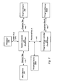
- the computer system includes a processor 100 coupled to a system controller 120 through a system bus 110.
- System controller 120 is coupled to main memory 130 through a memory bus 135.
- System controller 120 is also coupled to a graphics adapter 140 through a graphics bus 145.
- a peripheral controller 150 is coupled to system controller 120 through a peripheral bus A 155.
- Various peripheral devices such as 160A and 160B may be connected to peripheral bus A 155 and peripheral bus B 165, respectively.
- system controller 120 may be a Northbridge style integrated circuit which may be part of a chip set used in conjunction with processor 100.
- system controller 120 may be integrated with processor 100.
- memory 130 may be coupled directly to the processor 100.
- processor 100 is an example of an x86 class processor. However, in other examples, processor 100 may be any type of processor. Numerous alternative configurations are possible and are contemplated.
- processor 100 may have periods of idle time during which the system clock may continue to run but processor 100 is not processing data.
- logic transitions in a clocked system component may be a major source of power consumption in an integrated circuit.
- stopping or reducing the frequency of the clock signal during idle periods is one method of saving power.
- additional system power savings may be realized by stopping the internal clock of the chipsets and other peripheral components associated with processor 100.
- a signal may be activated which may alert processor 100 to stop or reduce its internal clock, thereby achieving additional system power savings.
- Processor 100 includes a clock circuit 200 coupled to a control circuit 204.
- Processor 100 is also coupled to receive reference clock signal 210 from clock generator 202.
- Clock circuit 200 is coupled to receive signal(s) 220 from control circuit 204 and is further configured to convey internal clock signal 230.
- Processor 100 is also shown coupled to system bus 110.
- clock generator circuit 202 and clock circuit 200 may include a locked loop circuit such as a phase locked loop or a delay locked loop.
- Clock circuit 200 receives external reference clock 210 and generates a varying PLL clock corresponding to the reference clock 210.
- Clock circuit 200 may adjust the phase and frequency to lock a feedback clock signal to the phase and the frequency of external reference clock 210.
- processor 100 may be configured to reduce or stop its internal clock in order to achieve power savings.
- Clock circuit 200 may include a counter from which different clock frequencies in powers of two may be derived. However, in order to achieve more linear transitions in clock frequencies, clock circuit 200 is further configured to derive further clock frequencies.
- Table 300 is shown illustrating an example of the operation of clock circuit 200.
- Table 300 includes six columns 301-306.
- Column 301 show a reference frequency of a clock signal received by circuit 200.
- reference frequency 301 may represent the maximum operating frequency of the processor's internal clock signal. In alternative examples, the maximum frequency of the processor's internal clock signal may not be equal to reference frequency 301.
- Column 302 shows a divisor applied to the reference frequency 301, and column 303 shows the result of dividing the reference frequency 301 by the corresponding divisor 302.
- the reference frequency is applied to a counter and the divisor is achieved by taking selected bits of the counter (i.e., the least significant bit of the counter corresponds to a divisor of two, the next least significant bit corresponds to a divisor of four, and so on.).
- deriving clock frequencies from a counter in this manner results in frequencies which are powers of two.
- four frequencies 303 may be achieved: 1000 MHz, 500 MHz, 250MHz, and 125 MHz.
- column 304 illustrates a method and mechanism whereby certain pulses of the frequency 303 are dropped or masked.
- circuit 200 is configured to drop N of M pulses of the clock signal 303, where M equals 8 and N is an integer from 0-M. In other embodiments, M may be an integer larger or smaller than 8. In this manner, additional effective divisors 305 may be achieved and further effective clock frequencies 306 may be derived from frequency 303.
- Fig. 3 utilizes particular frequencies 301, divisors 302, and dropped pulses 304, they are intended to be exemplary only. Those skilled in the art will recognize different combinations of reference frequencies 301, divisors 302 and dropped pulses 304 may be utilized to achieve any number of effective frequencies 306.
- Fig. 4A shows a graph with a y-axis representing frequency and x-axis representing time.
- Fig. 4A illustrates transitions between clock frequencies as powers of two. Such transitions may be achieved by utilizing a counter as described above.
- a transition from 1000 MHz to 500 MHz occurs (assuming a decrease in frequency is initiated).
- a transition 502B from 500 MHz to 250 MHz, and finally a transition 502C from 250 MHz to 125 MHz occurs.
- transition 502A from 1000 MHz to 500 MHz is abrupt and manifestly non-linear.
- a 50% drop in power results.
- a 100% increase in power results.
- Fig. 4B illustrates the effect of utilizing the dropped pulse method described above in Fig. 3 .
- Fig. 4B also shows a graph as in Fig. 4A wherein a frequency transition from 1000 MHz to 125 MHz occurs.
- numerous intermediate steps are in the transitions.
- the transition from 1000 MHz to 500 MHz occurs in four steps, 510A-510D.
- the transition from 500 MHz to 250 MHz occurs in two steps, 520A and 520B.
- the transition 510A-510D from 1000 MHz to 500 MHz shown in Fig. 4B is not so abrupt, but is much more linear.
- the transition 510A from 1000MHz to 875MHz results in a relatively small 12.5% drop in power.
- increasing frequency from 875MHz to 1000MHz involves an increase in power of 14.6%. In this manner, fluctuations in power may be reduced significantly.
- circuit 200 includes circuit 440, multiplexors 702, 770 and 780, and registers 730. Each of registers 730 are coupled to multiplexor 770 which is configured to convey signal 772 to multiplexor 780.
- Circuit 440 is coupled to receive a reference clock 210 and control signal(s) 220B. Circuit 440 is further coupled to convey data via paths 720 to multiplexors 702. Circuit 440 is also configured to generate a clock signal 710, which in one example is output from a VCO, which is then coupled as a select control signal 710 to multiplexor 770 and input to multiplexor 780.
- circuit 440 is configured to convey multiplexor select signal 790 to multiplexor 780 which conveys internal clock signal 230.
- registers 730A and 730B may be collectively referred to as registers 730.
- each of registers 730 is configured to store eight bits of data, though any suitable size for registers 730 may be chosen. Further, while the example shown utilizes two registers 730A-730B, other examples may utilize fewer or more registers.
- clock signal 710 may be a fixed frequency based on the received reference clock signal 210.
- circuit 440 may be configured to generate clock signal 710 at a variety of frequencies.
- clock signal 710 may be a multiple (greater than or less than one) of reference clock 210.
- the internal clock signal 230 conveyed by circuit 200 is equal to one of the two signals, 772 or 710, received by multiplexor 780. Control signal 790 is used to select which of the two signal will be conveyed as the internal clock signal 230.
- the internal clock signal 230 will be substantially equal to the clock signal 710 generated by circuit 440.
- internal clock 230 may have a frequency which is other than that of clock signal 710.
- each of registers 730 are coupled to multiplexor 770.
- registers 730 are configured as shift registers which are configured to shift their contents subsequent to conveying a value.
- registers 730 may optionally be configured as a circular shift register wherein values which are shifted out are shifted back in to registers 730 via paths 760.
- circuit 440 is configured to convey data via paths 720 for loading into registers 730.
- multiplexors 702 may be configured to select from a number of eight bit values conveyed via path 720 for simultaneous loading into registers 730.
- Circuit 440 may be configured to control which values are selected for conveyance from multiplexors 702.
- each of paths may be configured to convey 32 bits of data.
- four possible 8 bit load values may be conveyed to multiplexors 702 simultaneously. Values in a first position 792A and 792B or registers 730 are then conveyed via paths 750 to multiplexor 770.
- clock signal 710 is used as a select signal to multiplexor 770, values 792A and 792B will be alternately conveyed as signal 772.
- a few examples are given to illustrate how the register 730 values may be used to generate a variety of clock frequencies.
- Fig. 6A illustrates one example of how circuit 200 may be used to generate a variety of clock frequencies.
- Fig. 6A shows registers 730, multiplexor 770, clock signal 772 (labeled “Clock B") and selector 710 (labeled "Clock A”). Also illustrated are signals 630 and 670 representative of the values of Clock A and Clock B, respectively. Clock signals 630 and 670 are also marked with values from 0-7 indicating relative clock cycles.
- register 730A is loaded with all "1"s and register 730B is loaded with all "0"s. By loading the registers 730 in this manner, Clock B 772 assumes a frequency substantially equal to Clock A 710.
- Fig. 6B illustrates a loading of registers 730 which results in different frequencies between Clock A 710 and Clock B 770.
- a similar register 730 loading to that of Fig. 6A is used, except that two bits of register 730A have been changed from “1" to "0".
- registers 730 are configured in a circular manner, this pattern will repeat until the register load values are changed.
- the relationship between Clock A 710 and Clock B 772 is graphically depicted as signals 632 and 672, respectively. Given that eight bits are used for each register 730 in this example, we see that Clock B 772 has six clock cycles to every eight clock cycles of Clock A 710. Therefore, utilizing these particular register 730 load values, two out of every eight clock cycles of Clock A 710 are effectively masked. Viewed in another way, Clock B 772 has a frequency which is 75% that of Clock A 710. If Clock A 710 were 1000MHz, Clock B 772 would then be 750MHz.
- Fig. 6C shows an additional example using different register 730 load values.
- each of registers 730A and 730B are loaded with an identical, alternating sequence of bits.
- Clock B 772 assumes a frequency which is half that of Clock A 710.
- one or more pulses of Clock A 710 may be effectively dropped to create a Clock B 772 of a different frequency.
- Those skilled in the art will readily determine that a wide variety of clock frequencies for Clock B 772 may be generated by an appropriate selection of predetermined values placed in registers 730. Further, registers with more than eight entries may be used to create a wider variety of frequencies. By changing the contents of registers 730 at selected times, more linear increases and decreases of internal frequencies may be achieved.
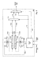
- Fig. 7 shows an embodiment of clock circuit 200 according to the invention.
- clock circuit 200 may be configured to receive a clock signal, count an integer number M of those clock signals, and drop or mask an integer number N out of those M clock pulses.
- clock circuit 200 is coupled to receive a reference clock signal 210 and control signals 220A-220B.
- Circuit 200 includes a control circuit 440, counter 520 comprising three storage elements 402A-402C, and multiplexor 420.
- Circuitry 440 is configured to receive a reference clock signal 210 and generate clock signal 510.
- circuit 440 may include a counter or other circuitry configured to derive frequencies for clock signal 510 from the reference frequency 210 in powers of two.
- the maximum frequency of clock signal 510 is half the frequency of reference clock 210, though other configurations are possible and are contemplated.
- counter 520 is configured to count pulses of clock signal 510 in groups of eight from 0-7.
- Signal 530A represents the least significant bit of counter 520
- signal 530B the next least significant bit
- signal 530C represents the most significant bit.
- Output signals from counter 520 are coupled to gates 410-N (where N is 1, 2, 5 and 7) and multiplexor 420.
- Gate 410-7 is configured to detect when a count of 7 is output from counter 520, gate 410-2 detects a count of 2, gate 410-5 detects a count of 5, and gate 410-1 detects a count of 1.
- OR gate 4-752 is configured to detect the assertion of three out of eight pulses.
- gate 4-752 detects when any of counts 7, 5, or 2 are asserted.
- OR gate 4-51 detects two out of eight pulses by detecting when counts 5 or 1 are asserted.
- output from each of gates 4-752,4-51,410-1, and counter signal 530A are coupled to multiplexor 420.
- Multiplexor 420 output 550 is coupled to AND gate 430 via inverted input.
- counter 520 output 530A is coupled to AND gate 430.
- multiplexor 420 includes four inputs, each corresponding to a number of clock pulses to be masked from the internal clock signal 230 which is conveyed by gate 430.
- the multiplexor 420 input corresponding to a selection of 0 is tied low.
- internal clock 230 will equal clock signal 530A.
- the output 550 will be asserted once every eight clock 530A pulses. Because the signal 550 is coupled to gate 430 via inverted input, the output from gate 430 will be masked off once every eight clock pulses.
- gate 430 output 230 will be masked twice every eight clock pulses.
- gate 430 output 230 will be masked three times each eight clock pulses when gate 4-752 is gated out the multiplexor 420. In this manner, the output from the multiplexor 420 may be used to control how many clock pulses are dropped or masked from the resulting clock signal 230.
- control signals 220A and 220B may be conveyed from processor 100 in response to detecting a change in power state is indicated. For example, in response to detecting a period of idle time, processor 100 convey signals 220A-220B to cause a reduction in the internal clock 230 frequency. Alternatively, while in a reduced power state, processor 100 may detect an interrupt or other signal indicating an increased power state is required. By coordinating the frequency of clock signal 510 with signal 220B, and the number of pulses to be dropped with signal 220A, processor 100 may achieve more linear transitions in operating frequencies.
- Fig. 8 depicts a number of signals corresponding the embodiment of Fig. 7 .
- Clock signal 510 is shown as operating at twice the frequency of clock signal 530A.
- the internal clock signal 230 is shown when 0, 1, 2, and 3 pulses are dropped or masked.
- Signals corresponding to counts of 1, 2, 5, and 7, which correspond to gates 410-1, 410-2, 410-5 and 410-7, respectively, are depicted in the example. While the counts of 1, 2, 5 and 7 have been described above, they are intended to be exemplary only.
- the counter 520 shown in Fig. 7 is configured to count pulses in groups of eight, counters of other sizes may be used as well. For example, counter 520 may be configured to count groups of sixteen pulses and the remaining circuitry of circuit 200 may be configured to detect one or more of those pulses.
- This invention may generally be applicable to computer system power management.
Landscapes
- Engineering & Computer Science (AREA)
- Theoretical Computer Science (AREA)
- Physics & Mathematics (AREA)
- General Engineering & Computer Science (AREA)
- General Physics & Mathematics (AREA)
- Power Sources (AREA)
- Manipulation Of Pulses (AREA)
- Circuit Arrangements For Discharge Lamps (AREA)
- Digital Transmission Methods That Use Modulated Carrier Waves (AREA)
- Synchronisation In Digital Transmission Systems (AREA)
Claims (8)
- Verfahren zum Erzeugen mehrerer Taktfrequenzen über einen Zeitraum in einer linearen Art und Weise, wobei das Verfahren Folgendes umfasst:Erzeugen eines ersten Taktsignals (510; 710) mit einer ersten Frequenz;Zählen von Sequenzen von Impulsen des ersten Taktsignals, wobei die Sequenzen eine festgelegte Anzahl von Impulsen aufweisen;Benutzen des ersten Taktsignals (510; 710), um ein zweites Taktsignal (230) mit einer zweiten Frequenz zu erzeugen;wobei das zweite Taktsignal (230) mit mehreren Taktfrequenzen erzeugt wird, wobei die mehreren Taktfrequenzen eine Anfangstaktsequenz, eine oder mehrere Zwischentaktfrequenzen und eine Endtaktfrequenz aufweisen; undwobei ein Übergang von der Anfangstaktsequenz über die Zwischentaktfrequenzen zur Endtaktsequenz in einer linearen Art und Weise durchgeführt wird, indem ausgewählte Impulse des ersten Taktsignals (510; 710) fallengelassen werden; undErkennen ausgewählter Impulse des ersten Taktsignals, wobei die ausgewählten Impulse bestimmten Zählwerten der Impulse innerhalb der festgelegten Anzahl von Impulsen entsprechen.
- Verfahren nach Anspruch 1, wobei das Benutzen des ersten Taktsignals (230) ein Benutzen des ersten Taktsignals zum Auswählen einer Sequenz von Werten aus einem Speicherelement (730) umfasst.
- Verfahren nach Anspruch 2, wobei das Speicherelement (730) ein erstes Schieberegister (730A) und ein zweites Schieberegister (730B) umfasst, und wobei die Sequenz von Werten abwechselnd aus den Registern (730A, 730B) ausgewählt wird.
- Verfahren nach Anspruch 1, 2 oder 3, wobei das Durchführen des Übergangs entweder ein Fallenlassen einer immer größeren Anzahl von Impulsen oder ein Fallenlassen einer immer kleineren Anzahl von Impulsen umfasst.
- Verfahren nach Anspruch 3, ferner umfassend Ändern eines Inhalts von wenigstens einem der Register (730A, 730B) zu einem ausgewählten Zeitpunkt, um das zweite Taktsignal (230) mit einer zunehmenden Frequenz zu erzeugen.
- Taktschaltkreis zum Erzeugen mehrerer Taktfrequenzen über einen Zeitraum in einer linearen Art und Weise, wobei der Taktschaltkreis Folgendes umfasst:einen ersten Schaltkreis (440), der zum Erzeugen eines ersten Taktsignals (510; 710) konfiguriert ist; undeinen Zähler, der zum Zählen von Sequenzen von Impulsen des ersten Taktsignals konfiguriert ist, wobei die Sequenzen eine festgelegte Anzahl von Impulsen aufweisen; undSchaltungen, die zum Benutzen des ersten Taktsignals (510; 710) konfiguriert sind, um ein zweites Taktsignal (230) zu erzeugen;wobei das zweite Taktsignal (230) mit mehreren Taktfrequenzen erzeugt wird, wobei die mehreren Taktfrequenzen eine Anfangstaktsequenz, eine oder mehrere Zwischentaktfrequenzen und eine Endtaktfrequenz aufweisen; undwobei ein Übergang von der Anfangstaktsequenz über die Zwischentaktfrequenzen zur Endtaktsequenz in einer linearen Art und Weise durchgeführt wird, indem ausgewählte Impulse des ersten Taktsignals (510; 710) fallengelassen werden; undwobei die Schaltungen dazu konfiguriert sind, die ausgewählten Impulse des ersten Taktsignals zu erkennen, wobei die ausgewählten Impulse bestimmten Zählwerten der Impulse innerhalb der festgelegten Anzahl von Impulsen entsprechen.
- Taktschaltkreis nach Anspruch 6, ferner umfassend ein Speicherelement (730), konfiguriert zum Speichern eines Bits-Musters, wobei die Schaltungen dazu konfiguriert sind, das erste Taktsignal (710) einzusetzen, um eine Sequenz von Werten von einem Speicherelement (730) auszuwählen.
- Taktschaltkreis nach Anspruch 7, wobei das Speicherelement (730) ein erstes (730A) und zweites (730B) Schieberegister umfasst und wobei die Schaltungen konfiguriert sind, um die Sequenz von Werten aus den Registern (730A, 730B) auf alternative Weise auszuwählen.
Applications Claiming Priority (3)
| Application Number | Priority Date | Filing Date | Title |
|---|---|---|---|
| US84566 | 2002-02-27 | ||
| US10/084,566 US6988217B1 (en) | 2002-02-27 | 2002-02-27 | Method and mechanism for generating a clock signal with a relatively linear increase or decrease in clock frequency |
| PCT/US2002/041658 WO2003073244A2 (en) | 2002-02-27 | 2002-12-20 | Frequency divider |
Publications (2)
| Publication Number | Publication Date |
|---|---|
| EP1479167A2 EP1479167A2 (de) | 2004-11-24 |
| EP1479167B1 true EP1479167B1 (de) | 2012-10-10 |
Family
ID=27765321
Family Applications (1)
| Application Number | Title | Priority Date | Filing Date |
|---|---|---|---|
| EP02794442A Expired - Lifetime EP1479167B1 (de) | 2002-02-27 | 2002-12-20 | Frequenzteiler |
Country Status (8)
| Country | Link |
|---|---|
| US (1) | US6988217B1 (de) |
| EP (1) | EP1479167B1 (de) |
| JP (1) | JP4255841B2 (de) |
| KR (1) | KR100945916B1 (de) |
| CN (1) | CN1315263C (de) |
| AU (1) | AU2002359876A1 (de) |
| TW (1) | TWI255976B (de) |
| WO (1) | WO2003073244A2 (de) |
Families Citing this family (18)
| Publication number | Priority date | Publication date | Assignee | Title |
|---|---|---|---|---|
| WO2005036751A1 (en) * | 2003-10-13 | 2005-04-21 | Koninklijke Philips Electronics N.V. | A frequency divider and an electronic device incorporating such a frequency divider |
| TWI254882B (en) | 2003-11-07 | 2006-05-11 | Via Tech Inc | Rate multiplication method and rate multiplier |
| CN100371885C (zh) * | 2003-11-17 | 2008-02-27 | 威盛电子股份有限公司 | 比率乘法的方法及比率乘法器 |
| US7288972B1 (en) * | 2004-03-08 | 2007-10-30 | Altera Corporation | Circuitry for synthesizing an arbitrary clock signal and methods for the synthesis thereof |
| US7610497B2 (en) * | 2005-02-01 | 2009-10-27 | Via Technologies, Inc. | Power management system with a bridge logic having analyzers for monitoring data quantity to modify operating clock and voltage of the processor and main memory |
| US20070263385A1 (en) * | 2005-03-21 | 2007-11-15 | He Shan Lide Electronic Enterprise Company Ltd. | Flexible Cable Light Capable Of Generating The Visual Effect Of Flowing Water |
| US7747881B2 (en) * | 2006-08-14 | 2010-06-29 | Globalfoundries Inc. | System and method for limiting processor performance |
| US7895421B2 (en) * | 2007-07-12 | 2011-02-22 | Globalfoundries Inc. | Mechanism for using performance counters to identify reasons and delay times for instructions that are stalled during retirement |
| US8504854B2 (en) | 2010-06-21 | 2013-08-06 | Advanced Micro Devices, Inc. | Managing multiple operating points for stable virtual frequencies |
| US9261949B2 (en) | 2010-10-29 | 2016-02-16 | Advanced Micro Devices, Inc. | Method for adaptive performance optimization of the soc |
| TWI454014B (zh) * | 2011-12-23 | 2014-09-21 | Kinpo Elect Inc | 太陽能電源管理模組、太陽能電源管理方法以及使用其之電子計算機 |
| US9411360B2 (en) | 2014-01-13 | 2016-08-09 | Apple Inc. | Method to manage current during clock frequency changes |
| US9582027B2 (en) | 2014-06-09 | 2017-02-28 | Qualcomm Incorporated | Clock swallowing device for reducing voltage noise |
| US9778676B2 (en) * | 2015-08-03 | 2017-10-03 | Qualcomm Incorporated | Power distribution network (PDN) droop/overshoot mitigation in dynamic frequency scaling |
| US10177773B2 (en) * | 2016-10-19 | 2019-01-08 | Stmicroelectronics International N.V. | Programmable clock divider |
| US10409317B2 (en) | 2017-06-05 | 2019-09-10 | Qualcomm Incorporated | Apparatus and methods for reducing clock-ungating induced voltage droop |
| US10735006B1 (en) * | 2019-06-25 | 2020-08-04 | Infineon Technologies Ag | Functional clock generation |
| US11709522B1 (en) * | 2020-09-16 | 2023-07-25 | Xilinx, Inc. | Power and temperature driven clock throttling |
Citations (2)
| Publication number | Priority date | Publication date | Assignee | Title |
|---|---|---|---|---|
| US5964881A (en) * | 1997-11-11 | 1999-10-12 | Advanced Micro Devices | System and method to control microprocessor startup to reduce power supply bulk capacitance needs |
| JP2002026723A (ja) * | 2000-04-04 | 2002-01-25 | Texas Instr Inc <Ti> | クロック信号の発生方法と装置 |
Family Cites Families (25)
| Publication number | Priority date | Publication date | Assignee | Title |
|---|---|---|---|---|
| US431566A (en) * | 1890-07-08 | Fire-escape | ||
| US3382460A (en) * | 1967-09-11 | 1968-05-07 | Sanders Associates Inc | Linearly swept frequency generator |
| GB1466603A (en) | 1974-11-06 | 1977-03-09 | Burroughs Corp | Flip-flop controlled clock gating system |
| JPS5941338B2 (ja) * | 1976-05-10 | 1984-10-06 | 日本電気株式会社 | クロツクパルス再生回路 |
| US4186637A (en) | 1977-09-22 | 1980-02-05 | Norlin Industries, Inc. | Tone generating system for electronic musical instrument |
| US4191942A (en) | 1978-06-08 | 1980-03-04 | National Semiconductor Corporation | Single slope A/D converter with sample and hold |
| GB2041591B (en) | 1979-01-31 | 1983-05-05 | Philips Electronic Associated | Frequency divider |
| US4284906A (en) | 1979-10-03 | 1981-08-18 | The United States Of America As Represented By The Secretary Of The Navy | Constant amplitude variable frequency synchronized linear ramp generator |
| US4471310A (en) * | 1982-01-04 | 1984-09-11 | At&T Bell Laboratories | Pulse generator having variable pulse occurrence rate |
| US4573017A (en) * | 1984-01-03 | 1986-02-25 | Motorola, Inc. | Unitary phase and frequency adjust network for a multiple frequency digital phase locked loop |
| US4855622A (en) | 1987-12-18 | 1989-08-08 | North American Philips Corporation, Signetics Division | TTL compatible switching circuit having controlled ramp output |
| US5517521A (en) * | 1993-06-25 | 1996-05-14 | Digital Wireless Corporation | Method and apparatus for synchronization between real-time sampled audio applications operating full-duplex over a half-duplex radio link |
| US5600347A (en) * | 1993-12-30 | 1997-02-04 | International Business Machines Corporation | Horizontal image expansion system for flat panel displays |
| US5485129A (en) * | 1995-01-20 | 1996-01-16 | Motorola, Inc. | Method and apparatus for digital modulation using pulse deletion |
| CN1061193C (zh) * | 1996-09-13 | 2001-01-24 | 清华大学 | 双自法频率预测恢复收端支路时钟的方法及装置 |
| US5825218A (en) | 1996-10-24 | 1998-10-20 | Stmicroelectronics, Inc. | Driver circuit including slew rate control system with improved voltage ramp generator |
| US5889436A (en) * | 1996-11-01 | 1999-03-30 | National Semiconductor Corporation | Phase locked loop fractional pulse swallowing frequency synthesizer |
| US6043692A (en) | 1998-07-13 | 2000-03-28 | Xilinx, Inc. | Circuit and method for generating clock signals with an incrementally reduced effective frequency |
| US6289067B1 (en) * | 1999-05-28 | 2001-09-11 | Dot Wireless, Inc. | Device and method for generating clock signals from a single reference frequency signal and for synchronizing data signals with a generated clock |
| GB9925593D0 (en) * | 1999-10-28 | 1999-12-29 | Sgs Thomson Microelectronics | Clock generator circuit |
| US6711694B1 (en) * | 2000-02-03 | 2004-03-23 | Telefonaktiebolaget Lm Ericsson(Publ) | Apparatus and method for generating a modulated clock signal including harmonics that exhibit a known sideband configuration |
| US6292062B1 (en) * | 2000-02-10 | 2001-09-18 | Silicon Wave, Inc. | Method and apparatus for implementing a high-precision interval timer utilizing multiple oscillators including a non-optimal oscillator |
| JP4446568B2 (ja) * | 2000-07-21 | 2010-04-07 | 富士通マイクロエレクトロニクス株式会社 | Pll周波数シンセサイザ回路 |
| EP1241788A1 (de) | 2001-03-13 | 2002-09-18 | STMicroelectronics Limited | Digitaler Frequenzteiler |
| JP4383045B2 (ja) * | 2002-12-27 | 2009-12-16 | アイシン・エィ・ダブリュ株式会社 | パワートレインの検査システム |
-
2002
- 2002-02-27 US US10/084,566 patent/US6988217B1/en not_active Expired - Lifetime
- 2002-12-20 CN CNB028283090A patent/CN1315263C/zh not_active Expired - Lifetime
- 2002-12-20 EP EP02794442A patent/EP1479167B1/de not_active Expired - Lifetime
- 2002-12-20 KR KR1020047012951A patent/KR100945916B1/ko not_active Expired - Lifetime
- 2002-12-20 AU AU2002359876A patent/AU2002359876A1/en not_active Abandoned
- 2002-12-20 WO PCT/US2002/041658 patent/WO2003073244A2/en not_active Ceased
- 2002-12-20 JP JP2003571872A patent/JP4255841B2/ja not_active Expired - Lifetime
-
2003
- 2003-02-26 TW TW092103985A patent/TWI255976B/zh not_active IP Right Cessation
Patent Citations (3)
| Publication number | Priority date | Publication date | Assignee | Title |
|---|---|---|---|---|
| US5964881A (en) * | 1997-11-11 | 1999-10-12 | Advanced Micro Devices | System and method to control microprocessor startup to reduce power supply bulk capacitance needs |
| JP2002026723A (ja) * | 2000-04-04 | 2002-01-25 | Texas Instr Inc <Ti> | クロック信号の発生方法と装置 |
| EP1248373A1 (de) * | 2000-04-04 | 2002-10-09 | Texas Instruments Incorporated | Vorrichtung und Verfahren zum Erzeugen eines Taktes aus einem eine beliebige Frequenz aufweisenden Takt |
Also Published As
| Publication number | Publication date |
|---|---|
| CN1315263C (zh) | 2007-05-09 |
| TWI255976B (en) | 2006-06-01 |
| WO2003073244A3 (en) | 2004-07-01 |
| KR20040086414A (ko) | 2004-10-08 |
| KR100945916B1 (ko) | 2010-03-05 |
| US6988217B1 (en) | 2006-01-17 |
| AU2002359876A8 (en) | 2003-09-09 |
| JP4255841B2 (ja) | 2009-04-15 |
| WO2003073244A2 (en) | 2003-09-04 |
| AU2002359876A1 (en) | 2003-09-09 |
| CN1620757A (zh) | 2005-05-25 |
| TW200304591A (en) | 2003-10-01 |
| EP1479167A2 (de) | 2004-11-24 |
| JP2005519367A (ja) | 2005-06-30 |
Similar Documents
| Publication | Publication Date | Title |
|---|---|---|
| EP1479167B1 (de) | Frequenzteiler | |
| US5964881A (en) | System and method to control microprocessor startup to reduce power supply bulk capacitance needs | |
| US5634117A (en) | Apparatus for operating a microprocessor core and bus controller at a speed greater than the speed of a bus clock speed | |
| US5359232A (en) | Clock multiplication circuit and method | |
| JP5997029B2 (ja) | 機能ブロックを含むSoCのクロック制御方法、それを具現したSoC、及びそれを含む半導体システム | |
| US7831006B2 (en) | Circuit to reduce transient current swings during mode transitions of high frequency/high power chips | |
| WO1994028477A1 (en) | Method and apparatus for power control in devices | |
| EP0613075B1 (de) | Mikroprozessor mit verteilten Taktgebern | |
| KR100231810B1 (ko) | 클럭 신호를 동적으로 발생하는 회로 및 방법 | |
| US6026498A (en) | Clock signal generator circuit using a logical result of an output of a computer and a source clock to generate plurality of clock signals | |
| US5822596A (en) | Controlling power up using clock gating | |
| EP0570158A2 (de) | Stabile Taktgeberschaltung mit Taktvervielfachung | |
| WO2005124516A2 (en) | Closed-loop control for performance tuning | |
| JP5987292B2 (ja) | 半導体集積回路装置及びそれを用いた電子機器 | |
| US6115443A (en) | Programmable frequency following device | |
| US7809974B2 (en) | Circuit to reduce power supply fluctuations in high frequency/high power circuits | |
| US7408420B2 (en) | Multi mode clock generator | |
| US20080195878A1 (en) | Control Scheme for Binary Control of a Performance Parameter | |
| US5594895A (en) | Method and apparatus for switching between clock generators only when activity on a bus can be stopped | |
| US20030212917A1 (en) | Microprocessor and operation mode switching method for the microprocessor | |
| JP6441166B2 (ja) | 半導体装置 | |
| US6212594B1 (en) | Timer with fixed and programmable interrupt periods | |
| EP1352304A2 (de) | Energieverwaltung für digitale verarbeitungsvorrichtung | |
| KR100738734B1 (ko) | 클록 생성기를 포함하는 칩 및 마이크로 프로세서 시스템 | |
| WO2006018801A1 (en) | Mixed signal integrated circuit |
Legal Events
| Date | Code | Title | Description |
|---|---|---|---|
| PUAI | Public reference made under article 153(3) epc to a published international application that has entered the european phase |
Free format text: ORIGINAL CODE: 0009012 |
|
| 17P | Request for examination filed |
Effective date: 20040913 |
|
| AK | Designated contracting states |
Kind code of ref document: A2 Designated state(s): AT BE BG CH CY CZ DE DK EE ES FI FR GB GR IE IT LI LU MC NL PT SE SI SK TR |
|
| AX | Request for extension of the european patent |
Extension state: AL LT LV MK RO |
|
| 17Q | First examination report despatched |
Effective date: 20110714 |
|
| GRAP | Despatch of communication of intention to grant a patent |
Free format text: ORIGINAL CODE: EPIDOSNIGR1 |
|
| GRAS | Grant fee paid |
Free format text: ORIGINAL CODE: EPIDOSNIGR3 |
|
| GRAA | (expected) grant |
Free format text: ORIGINAL CODE: 0009210 |
|
| AK | Designated contracting states |
Kind code of ref document: B1 Designated state(s): DE FR GB |
|
| REG | Reference to a national code |
Ref country code: GB Ref legal event code: FG4D |
|
| REG | Reference to a national code |
Ref country code: DE Ref legal event code: R096 Ref document number: 60243855 Country of ref document: DE Effective date: 20121206 |
|
| PLBE | No opposition filed within time limit |
Free format text: ORIGINAL CODE: 0009261 |
|
| STAA | Information on the status of an ep patent application or granted ep patent |
Free format text: STATUS: NO OPPOSITION FILED WITHIN TIME LIMIT |
|
| 26N | No opposition filed |
Effective date: 20130711 |
|
| REG | Reference to a national code |
Ref country code: FR Ref legal event code: ST Effective date: 20130830 |
|
| REG | Reference to a national code |
Ref country code: DE Ref legal event code: R097 Ref document number: 60243855 Country of ref document: DE Effective date: 20130711 |
|
| PG25 | Lapsed in a contracting state [announced via postgrant information from national office to epo] |
Ref country code: FR Free format text: LAPSE BECAUSE OF NON-PAYMENT OF DUE FEES Effective date: 20130102 |
|
| PGFP | Annual fee paid to national office [announced via postgrant information from national office to epo] |
Ref country code: DE Payment date: 20211027 Year of fee payment: 20 Ref country code: GB Payment date: 20211028 Year of fee payment: 20 |
|
| REG | Reference to a national code |
Ref country code: DE Ref legal event code: R071 Ref document number: 60243855 Country of ref document: DE |
|
| REG | Reference to a national code |
Ref country code: GB Ref legal event code: PE20 Expiry date: 20221219 |
|
| PG25 | Lapsed in a contracting state [announced via postgrant information from national office to epo] |
Ref country code: GB Free format text: LAPSE BECAUSE OF EXPIRATION OF PROTECTION Effective date: 20221219 |