EP1473960A2 - Selbstheilendes, bidirektionales, optisches WDM-Ringnetzwerk - Google Patents
Selbstheilendes, bidirektionales, optisches WDM-Ringnetzwerk Download PDFInfo
- Publication number
- EP1473960A2 EP1473960A2 EP04010021A EP04010021A EP1473960A2 EP 1473960 A2 EP1473960 A2 EP 1473960A2 EP 04010021 A EP04010021 A EP 04010021A EP 04010021 A EP04010021 A EP 04010021A EP 1473960 A2 EP1473960 A2 EP 1473960A2
- Authority
- EP
- European Patent Office
- Prior art keywords
- optical
- signals
- ring network
- ring
- wavelength
- Prior art date
- Legal status (The legal status is an assumption and is not a legal conclusion. Google has not performed a legal analysis and makes no representation as to the accuracy of the status listed.)
- Withdrawn
Links
Images




Classifications
-
- H—ELECTRICITY
- H04—ELECTRIC COMMUNICATION TECHNIQUE
- H04B—TRANSMISSION
- H04B10/00—Transmission systems employing electromagnetic waves other than radio-waves, e.g. infrared, visible or ultraviolet light, or employing corpuscular radiation, e.g. quantum communication
- H04B10/03—Arrangements for fault recovery
-
- H—ELECTRICITY
- H04—ELECTRIC COMMUNICATION TECHNIQUE
- H04J—MULTIPLEX COMMUNICATION
- H04J14/00—Optical multiplex systems
- H04J14/02—Wavelength-division multiplex systems
- H04J14/0287—Protection in WDM systems
- H04J14/0289—Optical multiplex section protection
- H04J14/0291—Shared protection at the optical multiplex section (1:1, n:m)
-
- H—ELECTRICITY
- H04—ELECTRIC COMMUNICATION TECHNIQUE
- H04B—TRANSMISSION
- H04B10/00—Transmission systems employing electromagnetic waves other than radio-waves, e.g. infrared, visible or ultraviolet light, or employing corpuscular radiation, e.g. quantum communication
- H04B10/03—Arrangements for fault recovery
- H04B10/032—Arrangements for fault recovery using working and protection systems
-
- H—ELECTRICITY
- H04—ELECTRIC COMMUNICATION TECHNIQUE
- H04B—TRANSMISSION
- H04B10/00—Transmission systems employing electromagnetic waves other than radio-waves, e.g. infrared, visible or ultraviolet light, or employing corpuscular radiation, e.g. quantum communication
- H04B10/25—Arrangements specific to fibre transmission
- H04B10/2581—Multimode transmission
-
- H—ELECTRICITY
- H04—ELECTRIC COMMUNICATION TECHNIQUE
- H04B—TRANSMISSION
- H04B10/00—Transmission systems employing electromagnetic waves other than radio-waves, e.g. infrared, visible or ultraviolet light, or employing corpuscular radiation, e.g. quantum communication
- H04B10/27—Arrangements for networking
- H04B10/275—Ring-type networks
-
- H—ELECTRICITY
- H04—ELECTRIC COMMUNICATION TECHNIQUE
- H04J—MULTIPLEX COMMUNICATION
- H04J14/00—Optical multiplex systems
- H04J14/02—Wavelength-division multiplex systems
- H04J14/0278—WDM optical network architectures
- H04J14/0283—WDM ring architectures
-
- H—ELECTRICITY
- H04—ELECTRIC COMMUNICATION TECHNIQUE
- H04J—MULTIPLEX COMMUNICATION
- H04J14/00—Optical multiplex systems
- H04J14/02—Wavelength-division multiplex systems
Definitions
- the 2x2 optical switching devices 110 to 180 maintain a bar state or no cross state, so that signals applied to the outer left input port i1 are transferred to the outer right output port o1, and the signals applied to the inner right input port i2 are transferred to the inner left output port o2.
- the optical switching devices 110 to 180 maintain a cross state, so that signals applied to the outer left input port i1 are transferred to the inner left output port o2, while signals applied to the inner right input port i2 are transferred to the outer right output port o1.
- the second left optical switching device sw21 or 130 is maintained in the cross state.
- FIG. 2 shows a structure of the conventional optical line distributor. It is assumed that an outer optical add/drop multiplexer is operated as one component in each node of the outer ring network 4, and an inner optical add/drop multiplexer is operated as one component in each node of the inner ring network 2. Therefore, each wavelength processed on the outer ring is ⁇ 1, ⁇ 2, ⁇ 3, ⁇ , ⁇ N, while one processed on the inner ring is ⁇ N+1, ⁇ N+2, ⁇ N+3, ⁇ , ⁇ 2N.
- the optical signals are directly transmitted without any loop-back when a link failure occurs.
- the bi-directional WDM self-healing optical ring network includes a plurality of nodes having optical add/drop multiplexers, each being provided on the first and second ring networks and includes a demultiplexer and a multiplexer, each of which has a capacity of 1xN; a pair of switching devices provided across the first and second ring networks and connected between the optical add/drop multiplexers and fiber optic links connected with another node; and, wavelength interleavers, each being provided on both ends of each optical add/drop multiplexer provided on the first and second ring networks.
- the interleaver further includes three ports, of which one port is connected to each switching device and allows for passing signals of all wavelength bands, another port allows for passing only signals of some wavelength bands processed on any one of the first and second ring networks, and the third port allows for passing only signals of the other wavelength bands processed on the other.
- optical signals with the wavelengths of ⁇ 1, ⁇ 3, ..., ⁇ 2N-1 are inputted into the optical add/drop multiplexer 210a of the outer ring network 4, while optical signals with the wavelengths of ⁇ 2, ⁇ 4, ..., ⁇ 2N are inputted into the optical add/drop multiplexer 210b of the inner ring network 2.
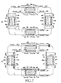
- the 2x2 optical switching device maintains a bar or no-cross state, so that signals applied to an outer-left input port i1 are propagated to an outer-right output port o1, and signals applied to an inner-right input port i2 are propagated to an inner-left output port o2.
- the optical signals with the wavelength bands of ⁇ 1, ⁇ 3, ⁇ , ⁇ 2N-1, which are transferred to the optical add/drop multiplexer 210a of the outer ring network 4 do no longer proceed past the optical switching device 120 toward the optical switching device 130.
- each optical add/drop multiplexer multiplexes or demultiplexes only signals which it must drop or add. That is, the optical add/drop multiplexer 210b processes only the optical signals with wavelengths of ⁇ 1, ⁇ 3, ⁇ , ⁇ 2N-1.
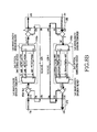
- the looped-back signals are connected using the wavelength interleavers without performing the multiplexing and demultiplexing at the optical add/drop multiplexers 210a to 240a; and 210b to 240b. Note that this is similar to the first embodiment of the present invention, except that the 4x4 optical switching devices 410 and 480 are designed to make it possible to separately switch only the signals, which are looped-back and then return.
- the optical signals with the wavelength bands of ⁇ 2, ⁇ 4, ⁇ , ⁇ 2N pass through a port 3 of the wavelength interleaver 316 and then demultiplexed. After passing through the wavelength interleaver 316, the optical signals with the wavelength bands of ⁇ 2, ⁇ 4, ⁇ , ⁇ 2N are demultiplexed and dropped through a 1xN demultiplexer of the optical add/drop multiplexer 210b according to each wavelength, and then multiplexed and added through an Nx1 mutiplexer of the optical add/drop multiplexer 210b, and finally outputted to the wavelength interleaver 314.
- the present invention is designed so that the channel interval of the transmitted optical signals in the bi-directional optical ring network is twice that of the prior art which in turn improves the transmission performance. Additionally, the optical signals passing through the link that does not experience failure can be transmitted normally without any interruption, which has occurred in the prior art, even if the loop-back technique is used to perform the protection switch.
- Each of the multiplexer and demultiplexer can reduce half the capacity required of the conventional optical add/drop multiplexers. Therefore, it is possible to provide an economical design choice and efficient operation to be implemented in the optical communication network.
Landscapes
- Engineering & Computer Science (AREA)
- Computer Networks & Wireless Communication (AREA)
- Signal Processing (AREA)
- Physics & Mathematics (AREA)
- Electromagnetism (AREA)
- Computing Systems (AREA)
- Optical Communication System (AREA)
- Small-Scale Networks (AREA)
Applications Claiming Priority (2)
| Application Number | Priority Date | Filing Date | Title |
|---|---|---|---|
| KR2003027671 | 2003-04-30 | ||
| KR10-2003-0027671A KR100520637B1 (ko) | 2003-04-30 | 2003-04-30 | 파장분할다중방식 자기치유 양방향 환형 광통신망 |
Publications (2)
| Publication Number | Publication Date |
|---|---|
| EP1473960A2 true EP1473960A2 (de) | 2004-11-03 |
| EP1473960A3 EP1473960A3 (de) | 2006-11-02 |
Family
ID=32985942
Family Applications (1)
| Application Number | Title | Priority Date | Filing Date |
|---|---|---|---|
| EP04010021A Withdrawn EP1473960A3 (de) | 2003-04-30 | 2004-04-27 | Selbstheilendes, bidirektionales, optisches WDM-Ringnetzwerk |
Country Status (4)
| Country | Link |
|---|---|
| US (1) | US7330650B2 (de) |
| EP (1) | EP1473960A3 (de) |
| JP (1) | JP3993580B2 (de) |
| KR (1) | KR100520637B1 (de) |
Cited By (2)
| Publication number | Priority date | Publication date | Assignee | Title |
|---|---|---|---|---|
| CN102684787A (zh) * | 2012-04-10 | 2012-09-19 | 郭磊 | 一个光通信的可靠性连接方案 |
| CN111903074A (zh) * | 2018-03-26 | 2020-11-06 | 日本电气株式会社 | 海底分支设备、光学海底缆线系统和光学通信方法 |
Families Citing this family (14)
| Publication number | Priority date | Publication date | Assignee | Title |
|---|---|---|---|---|
| US7634196B2 (en) * | 2004-10-06 | 2009-12-15 | Cisco Technology, Inc. | Optical add/drop multiplexer with reconfigurable add wavelength selective switch |
| US20060127086A1 (en) * | 2004-12-10 | 2006-06-15 | Ciena Corporation | Suppression of power transients in optically amplified links |
| CN100388708C (zh) * | 2005-01-01 | 2008-05-14 | 华为技术有限公司 | 分组光通道共享保护方法及其系统 |
| CN100454785C (zh) * | 2005-12-22 | 2009-01-21 | 华为技术有限公司 | 一种分组光通道共享保护的方法及装置 |
| WO2009012409A2 (en) * | 2007-07-17 | 2009-01-22 | Opvista Incorporated | Optical ring networks having node-to-node optical communication channels for carrying data traffic |
| CN101610129B (zh) * | 2009-07-09 | 2012-10-10 | 中兴通讯股份有限公司 | 实现完全无阻的波长无关性的可重构光分插复用装置 |
| US9485050B2 (en) | 2009-12-08 | 2016-11-01 | Treq Labs, Inc. | Subchannel photonic routing, switching and protection with simplified upgrades of WDM optical networks |
| US8705741B2 (en) | 2010-02-22 | 2014-04-22 | Vello Systems, Inc. | Subchannel security at the optical layer |
| JP5596397B2 (ja) * | 2010-04-02 | 2014-09-24 | 株式会社日立製作所 | 光伝送システム、光伝送方法 |
| EP2475121A1 (de) | 2011-01-10 | 2012-07-11 | Ntt Docomo, Inc. | Kommunikationssystem und Verfahren zur direkten Übertragung von Signalen zwischen Knoten eines Kommunikationssystems |
| US8542999B2 (en) | 2011-02-01 | 2013-09-24 | Vello Systems, Inc. | Minimizing bandwidth narrowing penalties in a wavelength selective switch optical network |
| EP2745153A4 (de) * | 2011-08-19 | 2015-05-20 | Avp Mfg & Supply Inc | Faseradapter für eine steckbaugruppe mit kleinem formfaktor |
| TW201412058A (zh) * | 2012-09-07 | 2014-03-16 | Etherwan Systems Inc | 環狀網路之備援系統與環狀網路之備援方法 |
| EP3632131A4 (de) * | 2017-05-30 | 2021-03-24 | Commscope Technologies LLC | Rekonfigurierbare optische netzwerke |
Family Cites Families (8)
| Publication number | Priority date | Publication date | Assignee | Title |
|---|---|---|---|---|
| US5633741A (en) | 1995-02-23 | 1997-05-27 | Lucent Technologies Inc. | Multichannel optical fiber communications |
| US6115155A (en) | 1996-10-29 | 2000-09-05 | Chorum Technologies Inc. | System for dealing with faults in an optical link |
| JP3175630B2 (ja) * | 1997-04-02 | 2001-06-11 | 日本電気株式会社 | 光通信用ノード及びこれにより構成されるリング構成の波長分割多重光伝送装置 |
| JP4031853B2 (ja) * | 1997-10-20 | 2008-01-09 | 富士通株式会社 | 双方向光通信用光伝送装置 |
| JPH11346189A (ja) | 1998-06-01 | 1999-12-14 | Oki Electric Ind Co Ltd | 光ノード |
| DE19828973A1 (de) * | 1998-06-29 | 1999-12-30 | Siemens Ag | Optisches 2-Faser-Ringnetz |
| JP2001044936A (ja) | 2000-01-01 | 2001-02-16 | Nec Corp | 光通信用ノード及びこれにより構成されるリング構成の波長多重光伝送装置 |
| KR100487215B1 (ko) * | 2003-01-03 | 2005-05-04 | 삼성전자주식회사 | 파장분할다중방식 자기치유 환형 광통신망 |
-
2003
- 2003-04-30 KR KR10-2003-0027671A patent/KR100520637B1/ko not_active Expired - Fee Related
-
2004
- 2004-02-18 US US10/781,037 patent/US7330650B2/en not_active Expired - Fee Related
- 2004-04-27 EP EP04010021A patent/EP1473960A3/de not_active Withdrawn
- 2004-04-30 JP JP2004135144A patent/JP3993580B2/ja not_active Expired - Fee Related
Cited By (3)
| Publication number | Priority date | Publication date | Assignee | Title |
|---|---|---|---|---|
| CN102684787A (zh) * | 2012-04-10 | 2012-09-19 | 郭磊 | 一个光通信的可靠性连接方案 |
| CN111903074A (zh) * | 2018-03-26 | 2020-11-06 | 日本电气株式会社 | 海底分支设备、光学海底缆线系统和光学通信方法 |
| CN111903074B (zh) * | 2018-03-26 | 2023-09-15 | 日本电气株式会社 | 海底分支设备、光学海底缆线系统和光学通信方法 |
Also Published As
| Publication number | Publication date |
|---|---|
| US20040218526A1 (en) | 2004-11-04 |
| JP2004336771A (ja) | 2004-11-25 |
| US7330650B2 (en) | 2008-02-12 |
| KR20040093831A (ko) | 2004-11-09 |
| JP3993580B2 (ja) | 2007-10-17 |
| KR100520637B1 (ko) | 2005-10-13 |
| EP1473960A3 (de) | 2006-11-02 |
Similar Documents
| Publication | Publication Date | Title |
|---|---|---|
| US5647035A (en) | Ring network communication structure on an optical carrier and reconfigurable node for said structure | |
| US8396361B2 (en) | Method for the protection of a passive optical transmission network as well as a passive optical transmission network with a corresponding protection mechanism | |
| JP3908225B2 (ja) | 波長分割多重方式の双方向自己回復環状光通信網 | |
| JP5004914B2 (ja) | 光クロスコネクト装置および光ネットワーク | |
| EP1473960A2 (de) | Selbstheilendes, bidirektionales, optisches WDM-Ringnetzwerk | |
| EP1126648A2 (de) | Ausrüstung, Transponder und Verfahren zur Faserübertragung | |
| US8903240B2 (en) | Scalable reconfigurable optical add-drop multiplexer | |
| EP0981870B1 (de) | Optische einfugungs/ausblendungsvorrichtung | |
| US20050286896A1 (en) | Hybrid optical ring network | |
| US7123830B2 (en) | WDM self-healing optical ring network | |
| US8521021B2 (en) | Method and apparatus for switching optical wavelengths | |
| US7437075B2 (en) | Integrated reconfigurable optical add/drop multiplexer | |
| EP1501225A2 (de) | System und Verfahren zur Übertragung von optischem Verkehr zwischen Ringnetzwerken | |
| US6859576B2 (en) | Optical cross-connect system | |
| US6768831B2 (en) | Optical add-drop multiplexing apparatus | |
| JP4209087B2 (ja) | 光アッド/ドロップ装置 | |
| US7120360B2 (en) | System and method for protecting traffic in a hubbed optical ring network | |
| US7113662B2 (en) | Optical filtering by using an add-drop node | |
| CN112088501B (zh) | 一种单纤环网结构 | |
| US6628440B1 (en) | System for diverting an optical component signal from a multiplexed optical signal | |
| US20050095001A1 (en) | Method and system for increasing network capacity in an optical network | |
| KR100547761B1 (ko) | 링형 광 네트워크의 광 애드/드롭 모듈 노드 구조 |
Legal Events
| Date | Code | Title | Description |
|---|---|---|---|
| PUAI | Public reference made under article 153(3) epc to a published international application that has entered the european phase |
Free format text: ORIGINAL CODE: 0009012 |
|
| 17P | Request for examination filed |
Effective date: 20040427 |
|
| AK | Designated contracting states |
Kind code of ref document: A2 Designated state(s): AT BE BG CH CY CZ DE DK EE ES FI FR GB GR HU IE IT LI LU MC NL PL PT RO SE SI SK TR |
|
| AX | Request for extension of the european patent |
Extension state: AL HR LT LV MK |
|
| PUAL | Search report despatched |
Free format text: ORIGINAL CODE: 0009013 |
|
| AK | Designated contracting states |
Kind code of ref document: A3 Designated state(s): AT BE BG CH CY CZ DE DK EE ES FI FR GB GR HU IE IT LI LU MC NL PL PT RO SE SI SK TR |
|
| AX | Request for extension of the european patent |
Extension state: AL HR LT LV MK |
|
| RIC1 | Information provided on ipc code assigned before grant |
Ipc: H04J 14/02 20060101AFI20060925BHEP |
|
| AKX | Designation fees paid |
Designated state(s): DE FR GB |
|
| 17Q | First examination report despatched |
Effective date: 20090904 |
|
| STAA | Information on the status of an ep patent application or granted ep patent |
Free format text: STATUS: THE APPLICATION IS DEEMED TO BE WITHDRAWN |
|
| 18D | Application deemed to be withdrawn |
Effective date: 20100115 |