EP1473737A1 - Non-volatile storage device and control method thereof - Google Patents
Non-volatile storage device and control method thereof Download PDFInfo
- Publication number
- EP1473737A1 EP1473737A1 EP03703249A EP03703249A EP1473737A1 EP 1473737 A1 EP1473737 A1 EP 1473737A1 EP 03703249 A EP03703249 A EP 03703249A EP 03703249 A EP03703249 A EP 03703249A EP 1473737 A1 EP1473737 A1 EP 1473737A1
- Authority
- EP
- European Patent Office
- Prior art keywords
- data
- physical
- address
- block
- stored
- Prior art date
- Legal status (The legal status is an assumption and is not a legal conclusion. Google has not performed a legal analysis and makes no representation as to the accuracy of the status listed.)
- Withdrawn
Links
Images






Classifications
-
- G—PHYSICS
- G11—INFORMATION STORAGE
- G11C—STATIC STORES
- G11C16/00—Erasable programmable read-only memories
- G11C16/02—Erasable programmable read-only memories electrically programmable
- G11C16/06—Auxiliary circuits, e.g. for writing into memory
- G11C16/10—Programming or data input circuits
-
- G—PHYSICS
- G06—COMPUTING OR CALCULATING; COUNTING
- G06F—ELECTRIC DIGITAL DATA PROCESSING
- G06F12/00—Accessing, addressing or allocating within memory systems or architectures
- G06F12/02—Addressing or allocation; Relocation
-
- G—PHYSICS
- G11—INFORMATION STORAGE
- G11C—STATIC STORES
- G11C16/00—Erasable programmable read-only memories
- G11C16/02—Erasable programmable read-only memories electrically programmable
- G11C16/06—Auxiliary circuits, e.g. for writing into memory
-
- G—PHYSICS
- G11—INFORMATION STORAGE
- G11C—STATIC STORES
- G11C16/00—Erasable programmable read-only memories
- G11C16/02—Erasable programmable read-only memories electrically programmable
- G11C16/06—Auxiliary circuits, e.g. for writing into memory
- G11C16/10—Programming or data input circuits
- G11C16/102—External programming circuits, e.g. EPROM programmers; In-circuit programming or reprogramming; EPROM emulators
- G11C16/105—Circuits or methods for updating contents of nonvolatile memory, especially with 'security' features to ensure reliable replacement, i.e. preventing that old data is lost before new data is reliably written
-
- G—PHYSICS
- G11—INFORMATION STORAGE
- G11C—STATIC STORES
- G11C16/00—Erasable programmable read-only memories
- G11C16/02—Erasable programmable read-only memories electrically programmable
- G11C16/06—Auxiliary circuits, e.g. for writing into memory
- G11C16/10—Programming or data input circuits
- G11C16/14—Circuits for erasing electrically, e.g. erase voltage switching circuits
- G11C16/16—Circuits for erasing electrically, e.g. erase voltage switching circuits for erasing blocks, e.g. arrays, words, groups
-
- G—PHYSICS
- G11—INFORMATION STORAGE
- G11C—STATIC STORES
- G11C2216/00—Indexing scheme relating to G11C16/00 and subgroups, for features not directly covered by these groups
- G11C2216/12—Reading and writing aspects of erasable programmable read-only memories
- G11C2216/14—Circuits or methods to write a page or sector of information simultaneously into a nonvolatile memory, typically a complete row or word line in flash memory
-
- G—PHYSICS
- G11—INFORMATION STORAGE
- G11C—STATIC STORES
- G11C2216/00—Indexing scheme relating to G11C16/00 and subgroups, for features not directly covered by these groups
- G11C2216/12—Reading and writing aspects of erasable programmable read-only memories
- G11C2216/18—Flash erasure of all the cells in an array, sector or block simultaneously
Definitions
- the present invention relates to a nonvolatile storage device utilizing a semiconductor memory, and a control method thereof.
- a storage device that has recently come to be used as a storage of a portable device handling audio data and video data, is equipped with a nonvolatile memory such as a flash memory that is updatable, highly portable, and does not require battery backup, and the like.
- FIG. 1 is a block diagram showing the structure of a memory card that is an existing nonvolatile storage device.
- a memory card 300 which is a device for storing data, being connected to a host apparatus 200 such as a personal computer and a digital camera, includes a controller 310 and a flash memory 320.
- the host apparatus 200 writes and reads data to and from the memory card 300, by use of a card control signal and a card data signal.
- card control signal and card data signal are inputted/outputted between the host apparatus 200 and the controller 310 inside the memory card 300.
- the controller 310 writes and reads data to and from the flash memory 320 by use of the memory control signal and memory data signal.
- the flash memory 320 connected to the controller 310 does not have to be one chip, and therefore that plural chips may be connected to the controller 310.
- FIG. 2 is a block diagram showing the configuration of the controller 310.
- the controller 310 is comprised of an MPU 311, a page RAM 312, an address conversion table 313, and an erase block table 314.
- the MPU 311 has an overall control over the controller 310, as well as controlling the data erasure from, data writing to, and data reading from the flash memory 320.
- the page RAM 312 is a volatile memory for temporarily storing data handled between the host apparatus 200 and the flash memory 320.
- the address conversion table 313 is a table for making a conversion between a host apparatus 200-specified address of data that is written to the flash memory 320 and a physical address in the flash memory 320.
- the erase block table 314 is a table that indicates, on a physical address basis, whether physical blocks in the flash memory 320 have already been erased or written. Information stored in the address conversion table 313 and the erase block table 314 is generated by reading out data of all the physical blocks in the flash memory 320 at the power-on time.
- FIG. 3 is a block diagram showing the configuration of the flash memory 320.
- the flash memory 320 is comprised of a page register 321, a memory cell array 323, a row decoder 324, and a command decoder 325.
- the memory cell array 323 is made up of all the memory cells contained in one chip of the flash memory 320.
- Memory cells constitute a page in units in which reading and writing can be performed simultaneously. Furthermore, a plurality of pages make up a physical block 322 that is an erasure unit.
- the page register 321 has the capacity equivalent to pages of memory cells, and holds write data to be inputted from the controller 310 and read data to be read out from memory cells.
- the row decoder 324 selects a page specified by the controller 310 at the time of data reading and writing, whereas it selects a physical block 322 specified by the controller 310 at the time of erasing data.
- the command decoder 325 executes a command from the controller 310 that is sent as a memory control signal.
- FIG. 4 is a schematic diagram showing example correspondence among data elements stored in the address conversion table 313, the erase block table 314, and the flash memory 320.
- Data in address 0 described in the address conversion table 313 is a physical address that corresponds to logical address 0. Since such data is "0001" in an example illustrated in FIG. 4(a), it indicates that data in logical address 0 is written in physical address 1 in the flash memory 320. Meanwhile, "FFFF" indicating a physical address that corresponds to logical address 1 is an invalid value that means that there is no data in logical address 1.
- "invalid value” is an arbitrary value that indicates invalidity and that is defined as invalid under the address conversion rule. An example of such value is a fixed value "0" and the maximum value "65535" in the case of 16-bit data. Furthermore, since data in address 2 in the address conversion table 313 is "0002", it indicates that data in logical address 2 is written in physical address 2 in the flash memory 320.
- the erase block table 314 shows the state of the respective physical blocks in the flash memory 320.
- the erase block table 314 holds, as address values, values that correspond to the respective physical addresses in the flash memory 320, and holds, as data values, whether the respective physical blocks in the flash memory 320 have already been erased or written.
- the erase block table 314 holds the value 1 when a physical block has already been erased, whereas it holds the value 0 when a physical block has already been written.
- data in address 0 in the erase block table 314 indicates whether a physical block corresponding to physical address 0 in the flash memory 320 has already been erased/written. Since such data is "1" in an example illustrated in FIG.
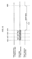
- FIG. 5 is a timing chart showing a write operation to be performed in such case
- FIG. 6 is a timing chart showing an erase operation to be performed in such case.
- upper signals are the card control signal and card data signal shown in FIG. 1, indicating that data is inputted from the host apparatus 200 to the memory card 300.
- Middle signals are the memory control signal and memory data signal shown in FIG. 3, indicating that data is inputted from the controller 310 to the flash memory 320.
- a lower signal is a memory control signal, indicating that data is outputted from the flash memory 320 to the controller 310.
- a description is given for the case as an example where data in logical address 0 in the memory card 300 is updated, in the state shown in FIG. 4(a).
- the host apparatus 200 sends, to the memory card 300, a write command 401 for logical address 0 as the card control signal at time t421, and starts transferring the write data as the card data signal at time t422.
- Such write data is to be stored into the page RAM 312 of the controller 310 in the memory card 300.
- the controller 310 Upon receipt of the write command 401 from the host apparatus 200, the controller 310 searches the erase block table 314 for an already erased physical block 322 to which it is possible to write the data. The controller 310 detects from the erase block table 314 that a physical block in physical address 0 is an already erased physical block 322.
- the controller 310 sends a write address specification command 403 for this data at time t423, so as to indicate the flash memory 320 that the write address is to be inputted thereafter.
- the command decoder 325 decodes the write address specification command 403, and controls the row decoder 324 to make it obtain the address to be inputted thereafter.
- the controller 310 sends a write address 404 to the flash memory 320 at time t424.
- the row decoder 324 obtains the inputted write address, and selects a specified page so that the data can be written to it.
- the command decoder 325 recognizes that the write address has been obtained, and controls the page register 321 to obtain the write address to be inputted thereafter.
- the controller 310 starts transferring the write data 405 from the page RAM 312 to the flash memory 320 at time t425.
- the command decoder 325 stores the inputted write data into the page register 321.
- the controller 310 sends a write execute command 406 to the flash memory 320 at time t427.
- the command decoder 325 starts, at time t427, writing the data stored in the page register 321 to memory cells of a page selected by the row decoder 324.
- the command decoder 325 sends, to the controller 310, a write busy 407 as the memory control signal indicating that writing is ongoing.
- a period defined as the write busy 407 indicates that no data shall be allowed to be newly read out, written, or erased during such period. This is because the command decoder 325 does not allow any commands to be inputted from the controller 310 for the reason that the same page that is subject to writing needs to remain selected by the row decoder 324 while such writing is taking place.
- the command decoder 325 releases the write busy 407 of the memory control signal. From then on, it is possible for commands to be inputted from the controller 310.
- controller 310 writes, to the other pages of the physical block 322 to which the above writing has been performed, data transferred from the host apparatus 200 in the above-described manner.
- the controller 310 obtains, from the address conversion table 313, a physical block in which the data in logical address 0 subject to the writing, was originally written. Since data in address 0 in the address conversion table 313 is "0001" in an example shown in FIG. 4(a), the physical block corresponding to physical address 1 is the location where the old data was written.
- the controller 310 sends an erase address specification command 411 for the physical block 322 corresponding to physical address 1 at time t431, so as to indicate the flash memory 320 that the erase address is to be inputted thereafter.
- the command decoder 325 decodes the erase address specification command 411, and controls the row decoder 324 to obtain the address to be inputted thereafter.
- the controller 310 sends an erase address 412 to the flash memory 320 at time t432.
- the row decoder 324 obtains the inputted erase address, and selects a specified physical block 322 so that the data can be erased.
- the controller 310 sends an erase execute command 413 to the flash memory 320 at time t433.
- the command decoder 325 starts, at time t434, erasing the physical block 322 selected by the row decoder 324.
- the command decoder 325 sends, to the controller 310, an erase busy 414 as the memory control signal indicating that erasure is ongoing.
- a period defined as the erase busy 414 indicates that no data shall be allowed to be newly read out, written, or erased during such period, as in the case of writing.
- the command decoder 325 releases the erase busy 414 of the memory control signal.
- FIG. 4(b) is a schematic diagram showing the state changed from the state shown in FIG. 4(a) by updating the data in logical address 0.
- the MPU 311 since physical block 322 to which the writing was performed this time is in address 0, the MPU 311 updates the data in address 0 in the erase block table 314 to "0" indicating that the block has already been written. Moreover, as shown in FIG. 4(b), the MPU 311 also updates the value of address 0 in the address conversion table 313 to "0000" that indicates the physical address of the physical block 322 to which the writing has performed this time. Furthermore, since the physical block 322 which was erased this time is in address 1, the MPU 311 updates the data in address 1 in the erase block table 314 to "1" indicating that the block has already been erased, as shown in FIG. 4(b).
- Data in the memory card 300 is updated by the host apparatus 200, as in the above-described manner.
- time required for update is approximately equal to the total of erase busy 414, time required to input write data 405, and write busy 407.
- the present invention has been conceived in view of the above circumstances, and it is an object of the present invention to provide a nonvolatile storage device and a control method thereof capable of maintaining data consistency even when some abnormality occurs while data is being updated, as well as capable of shortening the time required for updating data.
- the nonvolatile storage device is a nonvolatile storage device comprising: a nonvolatile storage unit having a plurality of physical blocks, each of which is made up of a plurality of pages for storing data; and a control unit operable to write, when updating the data stored in the storage unit, new data to an erased first physical block that is different from a second physical block in which old data is stored, wherein when updating the data stored in the storage unit, the control unit writes the new data to a page of the first physical block after erasing invalid data stored in said first physical block.
- the storage unit includes: a specification unit operable to select and specify one of the pages or one of the plurality of physical blocks; and a page holding unit operable to hold, in advance, data to be written to said one of the pages, and when updating the data stored in the storage unit, the control unit ( i ) erases the invalid data stored in the first physical block specified by the specification unit, ( ii ) transfers, to the page holding unit, the new data, while said erasure is being executed, and ( iii ) writes the new data to said first physical block after the erasure is finished.
- a specification unit operable to select and specify one of the pages or one of the plurality of physical blocks
- a page holding unit operable to hold, in advance, data to be written to said one of the pages, and when updating the data stored in the storage unit, the control unit ( i ) erases the invalid data stored in the first physical block specified by the specification unit, ( ii ) transfers, to the page holding unit, the new data, while said erasure is being
- the storage unit may include a plurality of storage areas, each of which has a management area and a data area, the management area may have an address conversion table and a valid block table which correspond to one of the storage areas which said management area belongs to, the address conversion table being used to make a conversion between a logical address and a physical address, and the valid block table indicating whether valid data is stored in the respective physical blocks, and the control unit may further include a table holding unit operable to hold the address conversion table and the valid block table.
- nonvolatile storage device with the above configuration
- nonvolatile memory and a control device thereof
- control method for a nonvolatile storage device that includes, as its steps, the characteristic units equipped to the nonvolatile storage device with the above configuration, and further as a program that causes a computer apparatus to execute these steps.
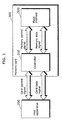
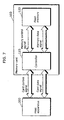
- FIG. 7 is a block diagram showing the structure of a memory card that is an embodiment of the nonvolatile storage device according to the present invention.
- a memory card 100 which is a device for storing data, being connected to a host apparatus 200 such as a personal computer and a digital camera, includes a controller 110 and a flash memory 120.
- the host apparatus 200 writes and reads data to and from the memory card 100, by use of a card control signal and a card data signal.
- card control signal and card data signal are inputted/outputted between the host apparatus 200 and the controller 110 inside the memory card 100.
- the controller 110 writes and reads data to and from the flash memory 120 by use of the memory control signal and memory data signal.
- the flash memory 120 connected to the controller 110 does not have to be one chip, and therefore that plural chips may be connected to the controller 110.
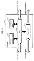
- FIG. 8 is a block diagram showing the configuration of the controller 110.
- the controller 110 is comprised of an MPU 111, a page RAM 112, an address conversion table 113, and a valid block table 114.
- the MPU 111 has an overall control over the controller 110, and also controls the data erasure from, data writing to, and data reading from the flash memory 120.
- the page RAM 112 is a volatile memory for temporarily storing data handled between the host apparatus 200 and the flash memory 120.
- the address conversion table 113 is a table for making a conversion between a host apparatus 200-specified address of data that is written to the flash memory 120 and a physical address in the flash memory 120.
- the valid block table 114 is a table that indicates whether data written on the flash memory 120 is valid or invalid on a physical address basis.
- invalid physical block means that valid data is not written to such block, and such physical block can either be in already written state or already erased state.
- information in the address conversion table 113 and the valid block table 114 is written in the management areas in the flash memory 120, and is read out by the MPU 111 from the flash memory 120 after the power is turned on or when necessary so as to be stored into the address conversion table 113 and the valid block table 114.
- the MPU 111 writes the updated data to the management areas in the flash memory 120, in response to such update.
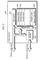
- FIG. 9 is a block diagram showing the configuration of the flash memory 120.
- the flash memory 120 is comprised of a page register 121, a memory cell array 123, a row decoder 124, and a command decoder 125.
- the memory cell array 123 is made up of all the memory cells contained in one chip of the flash memory 120. Memory cells constitute a page in units in which reading and writing can be carried out simultaneously. Furthermore, a plurality of pages make up a physical block 122 that is an erasure unit.
- the page register 121 has the capacity equivalent to pages of memory cells, and holds write data to be inputted from the controller 110 as well as read data to be read out from memory cells.
- the row decoder 124 selects a page specified by the controller 110 at the time of data reading and writing, whereas it selects a physical block 122 specified by the controller 110 at the time of erasing data.
- the command decoder 125 executes a command from the controller 110 that is sent as a memory control signal. Furthermore, the command decoder 125 allows a command to be inputted from the controller 110 to the flash memory 120 even while data erasure is ongoing, and exercises a control so that the command decoder 125 can operate even when commands come in the order of "write data" and "write address".
- FIG. 10 is a diagram showing an example logical configuration inside the memory cell array 123 of the flash memory 120.
- the memory cell array 123 is divided into plural areas in address order (four areas in an example shown in FIG. 10), and each of such areas has a management area and a data area.
- the address conversion table 113 and the valid block table 114 of the controller 110 are tables that describe information of one such area. Stated another way, an address conversation table 113 and a valid block table 114 corresponding to an area to which each management area belongs to is written in such management area.
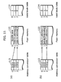
- FIG. 11 is a schematic diagram showing example correspondence among data elements stored in the address conversion table 113, the valid block table 114, and the flash memory 120.
- Data in address 0 described in the address conversion table 113 is a physical address that corresponds to logical address 0. Since such data is "0001" in an example illustrated in FIG. 11(a), it indicates that data in logical address 0 is written in physical address 1 in the flash memory 120. Meanwhile, "FFFF" indicating a physical address that corresponds to logical address 1 is an invalid value that means that there is no data in logical address 1.
- "invalid value” is an arbitrary value that indicates invalidity and that is defined as invalid under the address conversion rule. An example of such value is a fixed value "0" and the maximum value "65535" in the case of 16-bit data. Furthermore, since data in address 2 in the address conversion table 113 is "0002", it indicates that data in logical address 2 is written in physical address 2 in the flash memory 120.
- the valid block table 114 shows the state of data written to the flash memory 120.
- the valid block table 114 holds, as address values, values that correspond to the respective physical addresses in the flash memory 120, and holds, as data values, whether data written to the respective physical addresses in the flash memory 120 is valid data or invalid data.
- the valid block table 114 holds the value 0 when such data is valid, whereas it holds the value 1 when such data is invalid.
- data in address 0 in the valid block table 114 indicates whether data in physical address 0 in the flash memory 120 is valid or invalid. Since such data is "1" in an example illustrated in FIG. 11(a), it indicates that data in physical address 0 is invalid. Similarly, since each data in addresses 1 and 2 in the valid block table 114 is "0", it indicates that data in the respective physical addresses 1 and 2 in the flash memory 120 is valid.
- FIG. 12 is a flowchart showing an operation to be performed in the controller 110 in such case
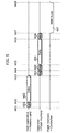
- FIG. 13 is a timing chart showing an operation to be performed in such case.
- upper signals are the card control signal and card data signal shown in FIG. 7, indicating that data is inputted from the host apparatus 200 to the memory card 100.
- Middle signals are the memory control signal and memory data signal shown in FIG. 3, indicating that data is inputted from the controller 110 to the flash memory 120.
- a lower signal is a memory control signal, indicating that data is outputted from the flash memory 120 to the controller 110.
- a description is given for the case as an example where data in logical address 0 in the memory card 100 is updated, in the state shown in FIG. 11(a).
- the host apparatus 200 sends, to the memory card 100, a write command 301 intended for logical address 0 as the card control signal at time t321, and starts transferring write data as the card data signal at time t322.
- Such write data is to be stored into the page RAM 112 of the controller 110 in the memory card 110.
- the controller 110 Upon receipt of the write command 301 from the host apparatus 200, the controller 110 searches the valid block table 114 for a physical block storing invalid data to which it is possible to write the data (Step S101). Upon detecting in the valid block table 114 that physical address 0 is a physical block 122 storing invalid data, the controller 110 sends, to the flash memory 120, an erase address specification command 303 for the physical block 122 corresponding to physical address 0 at time t322. Such erase address specification command 303 indicates that the erase address is to be inputted thereafter. The command decoder 125 decodes the erase address specification command 303, and controls the row decoder 124 to make it obtain the address to be inputted thereafter.
- the controller 110 sends an erase address 304 to the flash memory 120 at time t323.
- the row decoder 124 obtains the inputted erase address, and selects a specified physical block 122 so that the data can be erased.
- the controller 110 sends an erase execute command 305 to the flash memory 120 at time t324 (Step S102).
- the command decoder 125 starts, at time t325, erasing the physical block 122 selected by the row decoder 124.
- the command decoder 125 sends, to the controller 110, an erase busy 306 as the memory control signal indicating that erasure is ongoing.
- the erase busy 306 no data shall be allowed to be newly read out from, written to, or erased from a physical block 122 which are operations that require a selection by the row decoder 124, since the row decoder 124 needs to continuously select the physical block 122 subject to erasure.
- the controller 310 sends a write data input command 307 to the flash memory 120 at time t326, regardless of whether or not the erase busy 306 is inputted from the flash memory 120 as the memory control signal, so as to indicate the flash memory 120 that write data is to be inputted thereafter.
- the command decoder 125 decodes the write data input command 307, and controls the page register 121 to make it obtain the write data to be inputted thereafter.
- the controller 110 starts transferring write data 308 from the page RAM 112 to the flash memory 120 at time 327t (Step S103).
- the command decoder 125 stores the inputted write data into the page register 121.
- the data transferred here is write data to be written to a page included in the physical block 122 that is being erased. Note that the flash memory 120 is performing erase operation here, but it is possible to store write data since the page register 121 is not in use.
- the command decoder 125 releases the erase busy 306 of the memory control signal. From then on, it is possible for the row decoder 124 to select another physical block 122 or page.
- Step S104 and S105 the controller 110 sends a write address specification command 309 for the data transferred to the page register 121 at time t328, so as to indicate the flash memory 120 that a write address is to be inputted thereafter.
- the command decoder 125 decodes the write address specification command 309, and controls the row decoder 124 to obtain the address to be inputted thereafter.
- the controller 110 sends a write address 310 to the flash memory 120 at time t329.
- the row decoder 124 obtains the inputted write address, and selects a specified page so that the data can be written to it.
- the page to be specified here is a page included in the physical block on which the erase operation has finished above.
- the controller 110 sends a write execute command 311 to the flash memory 120 at time t330 (Step S106).
- the command decoder 125 starts, at time t331, writing the data stored in the page register 121 to memory cells in the page selected by the row decoder 124.
- the command decoder 125 sends, to the controller 110, a write busy 312 as the memory control signal indicating that writing is ongoing.
- the row decoder 124 keeps selecting a page to which data is to be written, and therefore no data shall be allowed to be newly read out from, written to, or erased from a physical block 122, which are operations that require a selection by the row decoder 124, as in the case of the period of the erase busy 306.
- the command decoder 125 releases the write busy 312 of the memory control signal.
- the controller 110 writes the data transferred from the host apparatus 200, to the other pages of the physical block 122 which has been erased in the above-described manner.
- FIG. 11(b) is a schematic diagram showing the state changed from the state shown in FIG. 11(a) by updating the data in logical address 0.
- the MPU 111 since the data corresponding to logical address 0 which was updated this time is "0001", as shown in FIG. 11(a), the MPU 111 updates the data in the corresponding address 1 in the valid block table 114 to "1", as shown in FIG. 11(b), indicating invalid data. Moreover, the MPU 111 also updates the value of address 0 in the address conversion table 113 to "0000", as shown in FIG. 11(b), that indicates the physical address of the physical block 122 to which the writing has performed this time. Then, the MPU 111 updates the data in address 0 in the valid block table 114 to "0" indicating valid data, as shown in FIG. 11(b).
- the MPU 111 writes the address conversation table 113 and valid block table 114 which have been updated in the above manner, to the management areas in the flash memory 120 in updated form.
- Data in the memory card 100 is updated by the host apparatus 200 side, as in the above-described manner. Note that when this writing is carried out, the updated old data of logical address 0 exits in the flash memory 120 as invalid data, and will not be erased until writing is performed to the physical block 122 that stores such old data, at the time of updating another data.
- the memory cell array 123 is logically divided into plural areas, and an address conversion table 113 and a valid block table 141 corresponding to each of such areas are written to the management area of each of the areas, the RAM of the controller 110 that reads in these tables is required to have only a small capacity.
- the controller 110 sends, to the flash memory 120, the write data input command 307 after the data transfer from the host apparatus 200 is finished, but the present invention is not limited to this. Therefore, the controller 110 may send the write data input command 307 after the erase execute command 305 is sent and before the data transfer from the host apparatus 200 is finished, for example. In this case, the controller 110 transfers the write data 308 from the page RAM 112 to the flash memory 120 after the data transfer from the host apparatus 200 is finished.
- the command decoder 125 exercises such a control as enables the flash memory 120 to operate even if commands are inputted in order of "write data” and "write address”, but the present invention is not limited to this. It is therefore possible to input commands in order of "write address” and "write data” by newly incorporating an address register to the flash memory 120, where a write address to be inputted during the period of the erase busy 306 is to be stored, and then by moving such write address to the row decoder 124 from the address register before the writing is executed.
- the nonvolatile storage device of the present invention it is possible to maintain consistency between data even if some abnormality occurs during the operation for updating data is taking place, since, when data stored in a storage unit is updated, data stored in an invalid physical block that is different from a physical block in which old data is stored, is erased first and then new data is written to a page in the erased physical block.
- the present invention which is capable of improving the usability of a nonvolatile storage device, is extremely useful in the present age when there is a widespread use of portable devices utilizing nonvolatile storage devices.
- the nonvolatile storage device is suited for use as a storage device that stores data of a portable device, such as a digital camera and a mobile phone, that handles audio data and video data.
Landscapes
- Engineering & Computer Science (AREA)
- Theoretical Computer Science (AREA)
- Computer Security & Cryptography (AREA)
- Physics & Mathematics (AREA)
- General Engineering & Computer Science (AREA)
- General Physics & Mathematics (AREA)
- Read Only Memory (AREA)
- Techniques For Improving Reliability Of Storages (AREA)
- Memory System (AREA)
Abstract
Description
Claims (11)
- A nonvolatile storage device comprising:wherein when updating the data stored in the storage unit, the control unit writes the new data to a page of the first physical block after erasing invalid data stored in said first physical block.a nonvolatile storage unit having a plurality of physical blocks, each of which is made up of a plurality of pages for storing data; anda control unit operable to write, when updating the data stored in the storage unit, new data to an erased first physical block that is different from a second physical block in which old data is stored,
- The nonvolatile storage device according to Claim 1,
wherein the storage unit includes:wherein when updating the data stored in the storage unit, the control unit ( i ) erases the invalid data stored in the first physical block specified by the specification unit, ( ii ) transfers, to the page holding unit, the new data, while said erasure is being executed, and ( iii ) writes the new data to said first physical block after the erasure is finished.a specification unit operable to select and specify one of the pages or one of the plurality of physical blocks; anda page holding unit operable to hold, in advance, data to be written to said one of the pages, - The nonvolatile storage device according to Claim 2,
wherein when writing the new data, the control unit transfers, to the specification unit, an address for specifying the page to which the new data is to be written, after transferring said new data to the page holding unit, and writes the new data to said one of the pages selected by the specification unit. - The nonvolatile storage device according to Claim 1,
wherein the storage unit includes a plurality of storage areas, each of which has a management area and a data area,
the management area has an address conversion table and a valid block table which correspond to one of the storage areas which said management area belongs to, the address conversion table being used to make a conversion between a logical address and a physical address, and the valid block table indicating whether valid data is stored in the respective physical blocks, and
the control unit further includes a table holding unit operable to hold the address conversion table and the valid block table. - The nonvolatile storage device according to Claim 4,
wherein the control unit ( i ) reads out, from the storage unit, the address conversion table and valid block table corresponding to each of the storage areas when necessary, so as to have the table holding unit hold said readout tables,
( ii ) specifies the first physical block in which the invalid data is stored with reference to the valid block table when updating the data stored in the storage unit, ( iii ) updates the address conversion table and the valid block table when said update of the data is finished, so as to reflect said update of the data on these tables, and ( iv ) writes the updated address conversion table and valid block table to the corresponding management area. - A nonvolatile memory, comprising:wherein the data to be written to said page is transferred to the page holding unit while said one of the physical blocks specified by the specification unit is being erased.a plurality of physical blocks, each of which is made up of a plurality of nonvolatile pages for storing data;a specification unit operable to select and specify one of the pages or one of the physical blocks; anda page holding unit operable to hold, in advance, data to be written to said one of the pages,
- A control device for controlling a nonvolatile memory that includes a plurality of physical blocks, each of which is made up of a plurality of nonvolatile pages for storing data, the control device comprising a control unit operable to write, when updating the data stored in the nonvolatile memory, new data to an erased first physical block that is different from a second physical block in which old data is stored,
wherein when updating the data stored in the nonvolatile memory, the control unit writes the new data to a page of the first physical block after erasing invalid data stored in said first physical block. - The control device according to Claim 7, further comprising a table holding unit operable to hold an address conversion table and a valid block table, the address conversion table being used to make a conversion between a logical address and a physical address, and the valid block table indicating whether valid data is stored in the respective physical blocks,
wherein the control unit specifies the first physical block in which the invalid data is stored with reference to the valid block table, when updating the data stored in the nonvolatile memory, and updates the address conversion table and the valid block table when said update of the data is finished, so as to reflect said update of the data on these tables. - A control method for controlling a nonvolatile storage device, the control method comprising a control step of writing new data to an erased first physical block that is different from a second physical block in which old data is stored, when data stored in a nonvolatile storage unit having a plurality of physical blocks is updated, each of said physical blocks being made up of a plurality of pages for storing data,
wherein in the control step, when the data is updated, the new data is written to a page of the first physical block, after invalid data stored in said first physical block is erased. - The control method for controlling the nonvolatile storage device according to Claim 9, further comprising a table holding step of holding an address conversion table and a valid block table, the address conversion table being used to make a conversion between a logical address and a physical address, and the valid block table indicating whether valid data is stored in the respective physical blocks,
wherein the control step includes:a specification step of specifying the first physical block in which the invalid data is stored with reference to the valid block table, when the data stored in the storage unit is updated; andan update step of updating the address conversion table and the valid block table when said update of the data is finished, so as to reflect said update of the data on these tables. - A program for updating data stored in a nonvolatile memory that includes a plurality of physical blocks, each of which is made up of a plurality of nonvolatile pages for storing data, the program causing a computer to execute a control step of writing new data to an erased first physical block that is different from a second physical block in which old data is stored,
wherein in the control step, when the data is updated, the new data is written to a page of the first physical block, after invalid data stored in said first physical block is erased.
Applications Claiming Priority (3)
| Application Number | Priority Date | Filing Date | Title |
|---|---|---|---|
| JP2002032081A JP2003233993A (en) | 2002-02-08 | 2002-02-08 | Rewriting method of nonvolatile storage device |
| JP2002032081 | 2002-02-08 | ||
| PCT/JP2003/001289 WO2003067605A1 (en) | 2002-02-08 | 2003-02-07 | Non-volatile storage device and control method thereof |
Publications (2)
| Publication Number | Publication Date |
|---|---|
| EP1473737A1 true EP1473737A1 (en) | 2004-11-03 |
| EP1473737A4 EP1473737A4 (en) | 2006-07-19 |
Family
ID=27677954
Family Applications (1)
| Application Number | Title | Priority Date | Filing Date |
|---|---|---|---|
| EP03703249A Withdrawn EP1473737A4 (en) | 2002-02-08 | 2003-02-07 | NON-VOLATILE MEMORY DEVICE AND ITS CONTROL METHOD |
Country Status (8)
| Country | Link |
|---|---|
| US (1) | US6944060B2 (en) |
| EP (1) | EP1473737A4 (en) |
| JP (1) | JP2003233993A (en) |
| KR (1) | KR100921282B1 (en) |
| CN (1) | CN100428363C (en) |
| CA (1) | CA2474739A1 (en) |
| TW (1) | TWI271622B (en) |
| WO (1) | WO2003067605A1 (en) |
Cited By (7)
| Publication number | Priority date | Publication date | Assignee | Title |
|---|---|---|---|---|
| WO2007131059A3 (en) * | 2006-05-05 | 2008-03-13 | Sandisk Corp | Non-volatile memory with background data latch caching during erase operations and methods therefor |
| WO2007130976A3 (en) * | 2006-05-05 | 2008-04-10 | Sandisk Corp | Non-volatile memory with background data latch caching during program operations and methods therefor |
| US7508721B2 (en) | 2005-04-01 | 2009-03-24 | Sandisk Corporation | Use of data latches in multi-phase programming of non-volatile memories |
| WO2008050337A3 (en) * | 2006-10-26 | 2009-08-27 | Sandisk Il Ltd. | Erase history-based flash writing method |
| EP2306416A1 (en) * | 2009-09-25 | 2011-04-06 | Incard SA | Improved method for pre-personalizing an IC Card |
| TWI427637B (en) * | 2006-05-05 | 2014-02-21 | Sandisk Technologies Inc | Non-volatile memory with background data latch caching during program operations and methods therefor |
| US8705286B2 (en) | 2005-04-01 | 2014-04-22 | SanDisk Technologies, Inc. | Method for non-volatile memory with background data latch caching during read operations |
Families Citing this family (23)
| Publication number | Priority date | Publication date | Assignee | Title |
|---|---|---|---|---|
| US20050204115A1 (en) * | 2004-01-30 | 2005-09-15 | Kiminori Matsuno | Semiconductor memory device, memory controller and data recording method |
| JP4097649B2 (en) * | 2004-12-09 | 2008-06-11 | ファナック株式会社 | Numerical controller |
| KR100876084B1 (en) * | 2007-02-13 | 2008-12-26 | 삼성전자주식회사 | Computing system capable of delivering deletion information to flash storage |
| KR100642892B1 (en) | 2005-07-19 | 2006-11-03 | 주식회사 하이닉스반도체 | Page buffer circuit with reduced area and its read and program operation method |
| JP4751163B2 (en) * | 2005-09-29 | 2011-08-17 | 株式会社東芝 | Memory system |
| CN100407336C (en) * | 2005-11-22 | 2008-07-30 | 武汉国光通信有限公司 | A data access method of non-volatile memory in embedded system |
| EP1966701A2 (en) * | 2005-12-21 | 2008-09-10 | Nxp B.V. | Memory with block-erasable locations |
| CN100533364C (en) * | 2006-08-08 | 2009-08-26 | 群联电子股份有限公司 | Generalized flash memory and method thereof |
| KR100754226B1 (en) * | 2006-08-22 | 2007-09-03 | 삼성전자주식회사 | Programming method of nonvolatile data storage device and device therefor |
| CN101571832B (en) * | 2008-04-29 | 2013-07-17 | 群联电子股份有限公司 | Data writing method, flash storage system using the method and its controller |
| US8843691B2 (en) | 2008-06-25 | 2014-09-23 | Stec, Inc. | Prioritized erasure of data blocks in a flash storage device |
| KR101466585B1 (en) | 2008-07-10 | 2014-11-28 | 삼성전자주식회사 | Memory device and managing method of memory device |
| JP2010129106A (en) * | 2008-11-25 | 2010-06-10 | Samsung Electronics Co Ltd | Nonvolatile semiconductor memory device |
| CN101446929A (en) * | 2008-12-01 | 2009-06-03 | 成都市华为赛门铁克科技有限公司 | Operating method for storing equipment, controller and communication system |
| JP4551958B2 (en) * | 2008-12-22 | 2010-09-29 | 株式会社東芝 | Semiconductor memory device and method for controlling semiconductor memory device |
| CN101782877B (en) * | 2009-01-16 | 2012-07-04 | 慧帝科技(深圳)有限公司 | Control device for controlling peripheral devices, non-volatile storage element and relevant method |
| KR20100115583A (en) * | 2009-04-20 | 2010-10-28 | 삼성전자주식회사 | Data storage systems |
| CN102541777B (en) * | 2010-12-13 | 2015-08-19 | 深圳市硅格半导体有限公司 | Flash data transmission control method and device based on DMA mapping |
| CN103680610A (en) * | 2012-09-03 | 2014-03-26 | 北京兆易创新科技股份有限公司 | Method and device for write operation of NAND Flash storage device with differential storage |
| KR101932920B1 (en) | 2012-09-14 | 2019-03-18 | 삼성전자 주식회사 | Host for controlling non-volatile memory crad, system including the same and operating method there-of |
| KR102254392B1 (en) | 2014-05-12 | 2021-05-25 | 삼성전자주식회사 | Operating method of memory controller and nonvolatile memory system including nonvolatile memory device and memory controller |
| TWI539282B (en) | 2014-10-13 | 2016-06-21 | 慧榮科技股份有限公司 | Non-volatile memory device and controller |
| US10854299B2 (en) * | 2018-05-31 | 2020-12-01 | Micron Technology, Inc. | Data erase operations for a memory system |
Family Cites Families (13)
| Publication number | Priority date | Publication date | Assignee | Title |
|---|---|---|---|---|
| JP3105092B2 (en) * | 1992-10-06 | 2000-10-30 | 株式会社東芝 | Semiconductor memory device |
| US6078520A (en) * | 1993-04-08 | 2000-06-20 | Hitachi, Ltd. | Flash memory control method and information processing system therewith |
| JPH07219720A (en) | 1993-10-01 | 1995-08-18 | Hitachi Maxell Ltd | Semiconductor memory device and control method thereof |
| JPH07153284A (en) * | 1993-11-29 | 1995-06-16 | Nec Corp | Non-volatile semiconductor memory and its control method |
| US5438549A (en) * | 1994-02-28 | 1995-08-01 | Intel Corporation | Nonvolatile memory with volatile memory buffer and a backup power supply system |
| US6418506B1 (en) * | 1996-12-31 | 2002-07-09 | Intel Corporation | Integrated circuit memory and method for transferring data using a volatile memory to buffer data for a nonvolatile memory array |
| JPH113270A (en) * | 1997-06-10 | 1999-01-06 | Hitachi Ltd | Flash memory device and method of writing data to flash memory |
| JPH113287A (en) * | 1997-06-12 | 1999-01-06 | Hitachi Ltd | Storage device and storage area management method used therein |
| JP3550293B2 (en) | 1997-12-26 | 2004-08-04 | 株式会社ルネサステクノロジ | High-speed rewritable storage device using nonvolatile memory and data rewriting method of the storage device |
| JP3421581B2 (en) * | 1998-06-29 | 2003-06-30 | 株式会社日立製作所 | Storage device using nonvolatile semiconductor memory |
| MY122279A (en) * | 1999-03-03 | 2006-04-29 | Sony Corp | Nonvolatile memory and nonvolatile memory reproducing apparatus |
| DE60037417D1 (en) * | 1999-07-28 | 2008-01-24 | Sony Corp | RECORDING SYSTEM, DATA RECORDING DEVICE, MEMORY DEVICE, AND DATA RECORDING METHOD |
| US6678203B1 (en) * | 1999-08-27 | 2004-01-13 | Sony Corporation | Editing apparatus, editing method, and non-volatile memory |
-
2002
- 2002-02-08 JP JP2002032081A patent/JP2003233993A/en active Pending
-
2003
- 2003-02-07 KR KR1020037012161A patent/KR100921282B1/en not_active Expired - Lifetime
- 2003-02-07 TW TW092102585A patent/TWI271622B/en not_active IP Right Cessation
- 2003-02-07 CA CA002474739A patent/CA2474739A1/en not_active Abandoned
- 2003-02-07 EP EP03703249A patent/EP1473737A4/en not_active Withdrawn
- 2003-02-07 US US10/493,383 patent/US6944060B2/en not_active Expired - Lifetime
- 2003-02-07 CN CNB038001292A patent/CN100428363C/en not_active Expired - Lifetime
- 2003-02-07 WO PCT/JP2003/001289 patent/WO2003067605A1/en not_active Ceased
Cited By (8)
| Publication number | Priority date | Publication date | Assignee | Title |
|---|---|---|---|---|
| US7508721B2 (en) | 2005-04-01 | 2009-03-24 | Sandisk Corporation | Use of data latches in multi-phase programming of non-volatile memories |
| US8705286B2 (en) | 2005-04-01 | 2014-04-22 | SanDisk Technologies, Inc. | Method for non-volatile memory with background data latch caching during read operations |
| WO2007131059A3 (en) * | 2006-05-05 | 2008-03-13 | Sandisk Corp | Non-volatile memory with background data latch caching during erase operations and methods therefor |
| WO2007130976A3 (en) * | 2006-05-05 | 2008-04-10 | Sandisk Corp | Non-volatile memory with background data latch caching during program operations and methods therefor |
| TWI427637B (en) * | 2006-05-05 | 2014-02-21 | Sandisk Technologies Inc | Non-volatile memory with background data latch caching during program operations and methods therefor |
| WO2008050337A3 (en) * | 2006-10-26 | 2009-08-27 | Sandisk Il Ltd. | Erase history-based flash writing method |
| EP2306416A1 (en) * | 2009-09-25 | 2011-04-06 | Incard SA | Improved method for pre-personalizing an IC Card |
| US8360326B2 (en) | 2009-09-25 | 2013-01-29 | Incard S.A. | Method for pre-personalizing an IC card |
Also Published As
| Publication number | Publication date |
|---|---|
| CN1498409A (en) | 2004-05-19 |
| TWI271622B (en) | 2007-01-21 |
| JP2003233993A (en) | 2003-08-22 |
| KR100921282B1 (en) | 2009-10-09 |
| US6944060B2 (en) | 2005-09-13 |
| EP1473737A4 (en) | 2006-07-19 |
| CA2474739A1 (en) | 2003-08-14 |
| TW200303462A (en) | 2003-09-01 |
| CN100428363C (en) | 2008-10-22 |
| WO2003067605A1 (en) | 2003-08-14 |
| US20040246779A1 (en) | 2004-12-09 |
| KR20040086500A (en) | 2004-10-11 |
Similar Documents
| Publication | Publication Date | Title |
|---|---|---|
| EP1473737A1 (en) | Non-volatile storage device and control method thereof | |
| JP3229345B2 (en) | Non-volatile IC memory | |
| US7800971B2 (en) | Flash memory devices and methods of programming the same by overlapping programming operations for multiple mats | |
| EP1739683B1 (en) | Space management for managing high capacity nonvolatile memory | |
| KR101579555B1 (en) | Page buffer program command and methods to reprogram pages without re-inputting data to a memory device | |
| US6556504B2 (en) | Nonvolatile semiconductor memory device and data input/output control method thereof | |
| KR100754226B1 (en) | Programming method of nonvolatile data storage device and device therefor | |
| KR100898653B1 (en) | Flash memory device and program method | |
| JP2006107719A (en) | Nonvolatile memory device and program method thereof | |
| US8085593B2 (en) | Method of inputting address in nonvolatile memory device and method of operating the nonvolatile memory device | |
| JP2004355699A (en) | Nonvolatile memory device and semiconductor memory device | |
| US6735126B1 (en) | Semiconductor memory | |
| US20090303800A1 (en) | Non-volatile memory control circuit | |
| JPH0817192A (en) | Position storage method by flash memory | |
| JP2005135544A (en) | Semiconductor recording medium and data erasing method of semiconductor recording medium | |
| JP2004273117A (en) | Semiconductor device and portable device equipped with composite flash memory | |
| KR20030045599A (en) | Method of controlling the operation of non-volatile semiconductor memory chips | |
| JP2008021335A (en) | Nonvolatile memory device, nonvolatile memory device writing method, and controller | |
| JP2005174468A (en) | Access control method of flash memory | |
| JP2000276883A (en) | Write-in circuit for non-volatile memory | |
| JP2000285092A (en) | Microcomputer | |
| JPH1173784A (en) | Semiconductor memory device and data reading method in its device | |
| JP2007048184A (en) | Memory card | |
| KR100676223B1 (en) | NAND flash memory controller | |
| JP2010165457A (en) | Flash memory device |
Legal Events
| Date | Code | Title | Description |
|---|---|---|---|
| PUAI | Public reference made under article 153(3) epc to a published international application that has entered the european phase |
Free format text: ORIGINAL CODE: 0009012 |
|
| 17P | Request for examination filed |
Effective date: 20040428 |
|
| AK | Designated contracting states |
Kind code of ref document: A1 Designated state(s): DE FR GB |
|
| RIC1 | Information provided on ipc code assigned before grant |
Ipc: G11C 16/16 20060101ALI20060324BHEP Ipc: G11C 16/10 20060101AFI20060324BHEP |
|
| A4 | Supplementary search report drawn up and despatched |
Effective date: 20060619 |
|
| 17Q | First examination report despatched |
Effective date: 20070628 |
|
| RAP1 | Party data changed (applicant data changed or rights of an application transferred) |
Owner name: PANASONIC CORPORATION |
|
| GRAP | Despatch of communication of intention to grant a patent |
Free format text: ORIGINAL CODE: EPIDOSNIGR1 |
|
| STAA | Information on the status of an ep patent application or granted ep patent |
Free format text: STATUS: THE APPLICATION IS DEEMED TO BE WITHDRAWN |
|
| 18D | Application deemed to be withdrawn |
Effective date: 20110323 |