EP1471611A2 - Flexibles Folienkabel - Google Patents
Flexibles Folienkabel Download PDFInfo
- Publication number
- EP1471611A2 EP1471611A2 EP04100565A EP04100565A EP1471611A2 EP 1471611 A2 EP1471611 A2 EP 1471611A2 EP 04100565 A EP04100565 A EP 04100565A EP 04100565 A EP04100565 A EP 04100565A EP 1471611 A2 EP1471611 A2 EP 1471611A2
- Authority
- EP
- European Patent Office
- Prior art keywords
- cable
- plug
- conductor tracks
- contact surfaces
- flat cable
- Prior art date
- Legal status (The legal status is an assumption and is not a legal conclusion. Google has not performed a legal analysis and makes no representation as to the accuracy of the status listed.)
- Withdrawn
Links
Images

Classifications
-
- H—ELECTRICITY
- H05—ELECTRIC TECHNIQUES NOT OTHERWISE PROVIDED FOR
- H05K—PRINTED CIRCUITS; CASINGS OR CONSTRUCTIONAL DETAILS OF ELECTRIC APPARATUS; MANUFACTURE OF ASSEMBLAGES OF ELECTRICAL COMPONENTS
- H05K1/00—Printed circuits
- H05K1/02—Details
- H05K1/11—Printed elements for providing electric connections to or between printed circuits
- H05K1/118—Printed elements for providing electric connections to or between printed circuits specially for flexible printed circuits, e.g. using folded portions
-
- H—ELECTRICITY
- H01—ELECTRIC ELEMENTS
- H01R—ELECTRICALLY-CONDUCTIVE CONNECTIONS; STRUCTURAL ASSOCIATIONS OF A PLURALITY OF MUTUALLY-INSULATED ELECTRICAL CONNECTING ELEMENTS; COUPLING DEVICES; CURRENT COLLECTORS
- H01R12/00—Structural associations of a plurality of mutually-insulated electrical connecting elements, specially adapted for printed circuits, e.g. printed circuit boards [PCB], flat or ribbon cables, or like generally planar structures, e.g. terminal strips, terminal blocks; Coupling devices specially adapted for printed circuits, flat or ribbon cables, or like generally planar structures; Terminals specially adapted for contact with, or insertion into, printed circuits, flat or ribbon cables, or like generally planar structures
- H01R12/70—Coupling devices
- H01R12/77—Coupling devices for flexible printed circuits, flat or ribbon cables or like structures
- H01R12/771—Details
- H01R12/775—Ground or shield arrangements
-
- H—ELECTRICITY
- H01—ELECTRIC ELEMENTS
- H01R—ELECTRICALLY-CONDUCTIVE CONNECTIONS; STRUCTURAL ASSOCIATIONS OF A PLURALITY OF MUTUALLY-INSULATED ELECTRICAL CONNECTING ELEMENTS; COUPLING DEVICES; CURRENT COLLECTORS
- H01R13/00—Details of coupling devices of the kinds covered by groups H01R12/70 or H01R24/00 - H01R33/00
- H01R13/64—Means for preventing incorrect coupling
- H01R13/642—Means for preventing incorrect coupling by position or shape of contact members
-
- H—ELECTRICITY
- H05—ELECTRIC TECHNIQUES NOT OTHERWISE PROVIDED FOR
- H05K—PRINTED CIRCUITS; CASINGS OR CONSTRUCTIONAL DETAILS OF ELECTRIC APPARATUS; MANUFACTURE OF ASSEMBLAGES OF ELECTRICAL COMPONENTS
- H05K2201/00—Indexing scheme relating to printed circuits covered by H05K1/00
- H05K2201/09—Shape and layout
- H05K2201/09209—Shape and layout details of conductors
- H05K2201/09654—Shape and layout details of conductors covering at least two types of conductors provided for in H05K2201/09218 - H05K2201/095
- H05K2201/09727—Varying width along a single conductor; Conductors or pads having different widths
-
- H—ELECTRICITY
- H05—ELECTRIC TECHNIQUES NOT OTHERWISE PROVIDED FOR
- H05K—PRINTED CIRCUITS; CASINGS OR CONSTRUCTIONAL DETAILS OF ELECTRIC APPARATUS; MANUFACTURE OF ASSEMBLAGES OF ELECTRICAL COMPONENTS
- H05K2201/00—Indexing scheme relating to printed circuits covered by H05K1/00
- H05K2201/10—Details of components or other objects attached to or integrated in a printed circuit board
- H05K2201/10007—Types of components
- H05K2201/10189—Non-printed connector
-
- H—ELECTRICITY
- H05—ELECTRIC TECHNIQUES NOT OTHERWISE PROVIDED FOR
- H05K—PRINTED CIRCUITS; CASINGS OR CONSTRUCTIONAL DETAILS OF ELECTRIC APPARATUS; MANUFACTURE OF ASSEMBLAGES OF ELECTRICAL COMPONENTS
- H05K2203/00—Indexing scheme relating to apparatus or processes for manufacturing printed circuits covered by H05K3/00
- H05K2203/16—Inspection; Monitoring; Aligning
- H05K2203/167—Using mechanical means for positioning, alignment or registration, e.g. using rod-in-hole alignment
Definitions
- the invention relates to a multi-pole connection cable, the as a flexible flat cable with several arranged side by side Traces formed and at least one cable end is provided with a plug, the conductor tracks electrically conductive at the end of the cable with contact surfaces of the connector are contacted and the flat cable and the connector means for centering the flat cable in the plug. Furthermore, the invention relates to a connector with in a Level contact surfaces for producing an electrical Connection to conductor tracks of a flat cable and an engagement element for centering the flat cable in the Plug.
- Such a cable and such a plug are from the GB-A-2 262 847.
- FPC films Flexible Printed Circuit
- the FPC film can be connected directly to the circuit board, i.e. the conductor tracks of the FPC film are covered with appropriate PCB conductor tracks soldered.
- the disadvantage here is that a quick disconnection is not easy is possible. That is why FPC foils are also inserted via foil connections connected to a circuit board.
- the circuit board has a corresponding plug, in the FPC film is inserted.
- Such plugs are often also as a ZIF connector (ZIF: Zero Insertion Force) or FFC connector (FFC: Flat Foil Cable).
- Multipole FFC connections with small distances between the conductor tracks or between the corresponding contact areas of the connector partially show different tolerances for the FPC film and the connector on. These different tolerances can lead to that conductor tracks of the FPC film are only slight or in In extreme cases, there is no longer any overlap with the contact surfaces of the Have connector. This can be immediate or early Failure of the device.
- the object of the invention is such a multi-pole connecting cable or to further develop such a connector, for an even more secure overlap between the contact surfaces of the plug and the conductor tracks of the cable to achieve high numbers of poles.
- the task is with a generic connection cable solved in that the width of the contact surfaces and / or the distance between adjacent contact areas and adapted to them the width of the conductor tracks and / or the distance between adjacent ones Traces is different.
- the risk of missing overlap between Conductor and associated contact area in the connector due the additive individual tolerances or deviations of the Conductor tracks and contact areas with increasing distance from this centering element. That is due to the different Width of the contact areas and / or the distance between adjacent ones Contact areas and adapted to the width of the conductor tracks and / or the distance between adjacent conductor tracks carried.
- the means for centering the flat cable preferably comprise one centrally arranged in the transverse direction of the flat cable Recess in which an engagement element of the plug engages.
- the recess and the engagement element is wedge-shaped.
- the connecting cable is preferably designed such that the Distance between adjacent tracks from the middle designed recess in both directions towards the cable edge grows. This can add up to the edge of the cable Tolerances are particularly well balanced.
- the Flat cable is designed as a ribbon-shaped plastic carrier, which is covered with conductor tracks on both sides. Because of the two-sided Assignment of the cable with conductor tracks will decrease the width of the cable and thus the required Installation space reached.
- a plug with contact surfaces arranged in one level for establishing an electrical connection to conductor tracks a flat cable and an engagement element for centering of the flat cable in the plug is thereby according to the invention characterized in that the width of the contact surfaces and / or the distance between adjacent contact surfaces is different. Further advantageous configurations are in the subclaims specified.
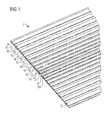
- the flat cable 1 shows a flat cable 1 with a large number of conductor tracks 2.
- the flat cable 1 is designed as a flexible film, to which the conductor tracks 2 are applied.
- the flat cable 1 has one attached centrally to the broad side of the cable Recess 3 on. Starting from the recess 3 takes the width of the conductor tracks 2 towards the edge of the cable continuously.
- the conductor track 2b thus has a larger one Width than the conductor track 2a, the conductor track 2c has one greater width than the conductor track 2b, the conductor track 2d has a greater width than the conductor track 2c, etc.
- the distances 4 between the conductor tracks 2 also grow with them increasing distance from the recess 3.
- Fig. 2 shows a connector 5, in the opening 6, the flat cable 1 is inserted.
- the connector 5 has a connector housing 7, which is drawn transparently in FIG. 2. in the Inside, the plug 5 has contact surfaces 8, which at inserted flat cable with the conductor tracks 4 in electrical conductive contact. The contact surfaces 8 are in not shown out on the connector 5 to the outside connect to a circuit board.
- the plug 5 furthermore has an engagement element 9, which in the Recess 3 of the flat cable 1 engages. This will create a Centering of the flat cable 1 in the connector 5 reached.
- the Distance 10 between the contact surfaces 8 is the width the conductor tracks 2 adapted. This increases the distance between the contact areas with increasing distance of the contact areas from the engaging element 9. The distance 10b is therefore larger than the distance 10a, the distance 10c is larger than the distance 10b etc.
- the positioning accuracy usually grows between Cable 1 and connector 5 with increasing distance from the engagement element 9 or the recess 3 by adding the individual tolerances the conductor tracks 2, the contact surfaces 8 and of the distances 4, 10. Due to the increasing width of the conductor tracks 2 or the distances 10 between the contact surfaces 8 with increasing distance from the recess 3 or the engagement element 9 takes these increasing deviations into account worn and also with the conductor tracks lying further on the edge 2k, 2u and contact areas 8k, 8u still a safe overlap reached.
Landscapes
- Engineering & Computer Science (AREA)
- Microelectronics & Electronic Packaging (AREA)
- Coupling Device And Connection With Printed Circuit (AREA)
- Multi-Conductor Connections (AREA)
Abstract
Description
- Fig. 1:
- ein als flexible Folie ausgebildetes Flachkabel,
- Fig. 2:
- einen erfindungsgemäßen Stecker .
Claims (10)
- Mehrpoliges Verbindungskabel, das als flexibles Flachkabel (1) mit mehreren nebeneinander angeordneten Leiterbahnen (2) ausgebildet und an mindestens einem Kabelende mit einem Stecker (5) versehen ist, wobei die Leiterbahnen (2) am Kabelende elektrisch leitend mit Kontaktflächen (8) des Steckers (5) kontaktiert sind und das Flachkabel (2) und der Stecker (5) Mittel zum Zentrieren des Flachkabels in dem Stecker (5) aufweisen, dadurch gekennzeichnet, dass die Breite der Kontaktflächen (8) und/oder der Abstand (10) benachbarter Kontaktflächen (8) sowie daran angepasst die Breite der Leiterbahnen (2) und/oder der Abstand (4) benachbarter Leiterbahnen (2) unterschiedlich ist.
- Verbindungskabel nach Anspruch 1, dadurch gekennzeichnet, dass die Mittel zum Zentrieren des Flachkabels (1) eine mittig in Querrichtung des Flachkabels (1) angeordnete Aussparung (3) umfassen, in die ein Eingriffselement (9) des Steckers (5) eingreift.
- Verbindungskabel nach Anspruch 2, dadurch gekennzeichnet, dass die Aussparung (3) und das Eingriffselement (9) keilförmig ausgebildet sind.
- Verbindungskabel nach einem der vorhergehenden Ansprüche, dadurch gekennzeichnet, dass der Abstand (4) zwischen benachbarten Leiterbahnen (2) von der mittig ausgelegten Aussparung (3) in beide Richtungen zum Kabelrand hin anwächst.
- Verbindungskabel nach einem der vorhergehenden Ansprüche, dadurch gekennzeichnet, dass das Flachkabel (1) als bandförmiger Kunststoffträger ausgebildet ist, der beidseitig mit Leiterbahnen (2) belegt ist.
- Verbindungskabel nach einem der vorhergehenden Ansprüche, dadurch gekennzeichnet, dass das Flachkabel (2) als flexible Folie ausgebildet ist.
- Stecker mit in einer oder mehreren Ebenen angeordneten Kontaktflächen (8) zur Herstellung einer elektrischen Verbindung zu Leiterbahnen (2) eines Flachkabels (1) und einem Eingriffselement (9) zur Zentrierung des Flachkabels (1) in dem Stecker (5), dadurch gekennzeichnet, dass die Breite der Kontaktflächen (8) und/oder der Abstand (10) benachbarter Kontaktflächen (8) unterschiedlich ist.
- Stecker nach Anspruch 7, dadurch gekennzeichnet, dass das Eingriffselement (9) mittig zur Kabelaufnahmeöffnung (6) des Steckers (5) angeordnet ist.
- Stecker nach einem der vorhergehenden Ansprüche, dadurch gekennzeichnet, dass das Eingriffselement (9) keilförmig ausgebildet ist.
- Stecker nach einem der vorhergehenden Ansprüche 8 oder 9, dadurch gekennzeichnet, dass der Abstand (10) zwischen benachbarten Kontaktflächen (8) von dem mittig angeordneten Eingriffselement (9) in beide Richtung hin anwächst.
Applications Claiming Priority (2)
| Application Number | Priority Date | Filing Date | Title |
|---|---|---|---|
| DE10314909A DE10314909A1 (de) | 2003-04-01 | 2003-04-01 | Flexibles Folienkabel |
| DE10314909 | 2003-04-01 |
Publications (2)
| Publication Number | Publication Date |
|---|---|
| EP1471611A2 true EP1471611A2 (de) | 2004-10-27 |
| EP1471611A3 EP1471611A3 (de) | 2006-01-25 |
Family
ID=32946362
Family Applications (1)
| Application Number | Title | Priority Date | Filing Date |
|---|---|---|---|
| EP04100565A Withdrawn EP1471611A3 (de) | 2003-04-01 | 2004-02-13 | Flexibles Folienkabel |
Country Status (2)
| Country | Link |
|---|---|
| EP (1) | EP1471611A3 (de) |
| DE (1) | DE10314909A1 (de) |
Family Cites Families (6)
| Publication number | Priority date | Publication date | Assignee | Title |
|---|---|---|---|---|
| DE7406973U (de) * | 1974-02-28 | 1974-05-30 | Kabel Und Lackdrahtfabriken Gmbh | Flachkabel |
| JP3088169B2 (ja) * | 1991-12-27 | 2000-09-18 | タイコエレクトロニクスアンプ株式会社 | 可撓性平形ケーブル用コネクタ |
| US5704793A (en) * | 1995-04-17 | 1998-01-06 | Teradyne, Inc. | High speed high density connector for electronic signals |
| DE19819056C1 (de) * | 1998-04-29 | 1999-11-18 | Kostal Leopold Gmbh & Co Kg | Steckverbinder für elektrische Flachleitungen |
| US20020157865A1 (en) * | 2001-04-26 | 2002-10-31 | Atsuhito Noda | Flexible flat circuitry with improved shielding |
| DE10124610A1 (de) * | 2001-05-21 | 2002-11-28 | Stocko Contact Gmbh & Co Kg | Steckverbinder, insbesondere zum Kontaktieren einer unterschiedlich ausgebildete Kontaktstellen aufweisenden elektrischen Leitung, und Anordnung aus Steckverbinder und elektrischen Leitung |
-
2003
- 2003-04-01 DE DE10314909A patent/DE10314909A1/de not_active Ceased
-
2004
- 2004-02-13 EP EP04100565A patent/EP1471611A3/de not_active Withdrawn
Also Published As
| Publication number | Publication date |
|---|---|
| EP1471611A3 (de) | 2006-01-25 |
| DE10314909A1 (de) | 2004-10-21 |
Similar Documents
| Publication | Publication Date | Title |
|---|---|---|
| DE3908481C2 (de) | ||
| DE69212725T2 (de) | Verbinder mit Erdungsanordnung | |
| WO2015035979A1 (de) | Steckverbinder | |
| CH628484A5 (de) | Verfahren und kontaktleiste zur herstellung gasdichter verbindungen fuer eine gedruckte rueckwandverdrahtung. | |
| EP0582960B1 (de) | HF-Koaxial-Steckverbindung | |
| EP2277242B1 (de) | Messerleisten-kontaktierung über zwischenleiterplatten | |
| EP3698438B1 (de) | Vorrichtung zur elektrischen kontaktierung | |
| DE69923652T2 (de) | Modularer gefilterter Verbinder | |
| DE102006031129B4 (de) | Gerätesystem mit auf einer Tragschiene montierten elektrischen Gerätemodulen und in der Tragschine angeordneter BUS-Leitung | |
| DE2405464A1 (de) | Vielfachsteckverbinder zur herstellung mehrerer elektrischer verbindungen | |
| EP2193576B1 (de) | Steckmittel, steckverbinder und verfahren zur herstellung des steckmittels | |
| EP1175712B1 (de) | Leiterplatten-steckverbinder | |
| DE3730662A1 (de) | Anschlussvorrichtung der fernmeldetechnik | |
| DE102004056866A1 (de) | Extrudierte Flachleitung sowie Verfahren zum Erzeugen einer extrudierten Flachleitung | |
| DE102011001486A1 (de) | Leiterplatten-Direktverbinder und Leiterplattenanordnung | |
| DE102021120385A1 (de) | Oberflächenmontagetechnik-Anschluss-Header und Verfahren zum Bereitstellen einer elektrischen Verbindung zu einer Leiterplatte | |
| EP1168526B1 (de) | Leiterplattensteckverbindung | |
| DE3444667A1 (de) | Kontaktbruecke fuer in gleicher ebene angeordnete leiterplatten in elektrischen und elektronischen geraeten und anlagen | |
| DE19858534A1 (de) | Elektrischer Verbinder | |
| DE10314909A1 (de) | Flexibles Folienkabel | |
| DE2513640B2 (de) | Mehrpolige codierte Steckverbindung | |
| DE7012569U (de) | Schaltungsanordnung fuer ein geraet der nachrichtentechnik. | |
| DE19715437C2 (de) | Elektrische Verteilervorrichtung mit Gemeinschaftsleiter | |
| DE8908973U1 (de) | Eine aus mindestens aus zwei parallel zueinander angeordneten Leiterplatten bestehende Baugruppe mit elektrisch leitender Verbindung | |
| EP3949024A1 (de) | Steckverbinder |
Legal Events
| Date | Code | Title | Description |
|---|---|---|---|
| PUAI | Public reference made under article 153(3) epc to a published international application that has entered the european phase |
Free format text: ORIGINAL CODE: 0009012 |
|
| AK | Designated contracting states |
Kind code of ref document: A2 Designated state(s): AT BE BG CH CY CZ DE DK EE ES FI FR GB GR HU IE IT LI LU MC NL PT RO SE SI SK TR |
|
| AX | Request for extension of the european patent |
Extension state: AL LT LV MK |
|
| PUAL | Search report despatched |
Free format text: ORIGINAL CODE: 0009013 |
|
| AK | Designated contracting states |
Kind code of ref document: A3 Designated state(s): AT BE BG CH CY CZ DE DK EE ES FI FR GB GR HU IE IT LI LU MC NL PT RO SE SI SK TR |
|
| AX | Request for extension of the european patent |
Extension state: AL LT LV MK |
|
| RIC1 | Information provided on ipc code assigned before grant |
Ipc: H01R 12/24 20060101AFI20051202BHEP |
|
| 17P | Request for examination filed |
Effective date: 20060220 |
|
| AKX | Designation fees paid |
Designated state(s): DE FR GB IT |
|
| RAP1 | Party data changed (applicant data changed or rights of an application transferred) |
Owner name: CONTINENTAL AUTOMOTIVE GMBH |
|
| STAA | Information on the status of an ep patent application or granted ep patent |
Free format text: STATUS: THE APPLICATION IS DEEMED TO BE WITHDRAWN |
|
| 18D | Application deemed to be withdrawn |
Effective date: 20100901 |