EP1469584A2 - Non-contact electrical power transmission system having function of making load voltage constant - Google Patents
Non-contact electrical power transmission system having function of making load voltage constant Download PDFInfo
- Publication number
- EP1469584A2 EP1469584A2 EP04014754A EP04014754A EP1469584A2 EP 1469584 A2 EP1469584 A2 EP 1469584A2 EP 04014754 A EP04014754 A EP 04014754A EP 04014754 A EP04014754 A EP 04014754A EP 1469584 A2 EP1469584 A2 EP 1469584A2
- Authority
- EP
- European Patent Office
- Prior art keywords
- load
- voltage
- current
- capacitor
- circuit
- Prior art date
- Legal status (The legal status is an assumption and is not a legal conclusion. Google has not performed a legal analysis and makes no representation as to the accuracy of the status listed.)
- Granted
Links
Images


Classifications
-
- H—ELECTRICITY
- H02—GENERATION; CONVERSION OR DISTRIBUTION OF ELECTRIC POWER
- H02M—APPARATUS FOR CONVERSION BETWEEN AC AND AC, BETWEEN AC AND DC, OR BETWEEN DC AND DC, AND FOR USE WITH MAINS OR SIMILAR POWER SUPPLY SYSTEMS; CONVERSION OF DC OR AC INPUT POWER INTO SURGE OUTPUT POWER; CONTROL OR REGULATION THEREOF
- H02M1/00—Details of apparatus for conversion
- H02M1/08—Circuits specially adapted for the generation of control voltages for semiconductor devices incorporated in static converters
- H02M1/088—Circuits specially adapted for the generation of control voltages for semiconductor devices incorporated in static converters for the simultaneous control of series or parallel connected semiconductor devices
- H02M1/096—Circuits specially adapted for the generation of control voltages for semiconductor devices incorporated in static converters for the simultaneous control of series or parallel connected semiconductor devices the power supply of the control circuit being connected in parallel to the main switching element
-
- H—ELECTRICITY
- H02—GENERATION; CONVERSION OR DISTRIBUTION OF ELECTRIC POWER
- H02J—CIRCUIT ARRANGEMENTS OR SYSTEMS FOR SUPPLYING OR DISTRIBUTING ELECTRIC POWER; SYSTEMS FOR STORING ELECTRIC ENERGY
- H02J50/00—Circuit arrangements or systems for wireless supply or distribution of electric power
- H02J50/10—Circuit arrangements or systems for wireless supply or distribution of electric power using inductive coupling
-
- H—ELECTRICITY
- H02—GENERATION; CONVERSION OR DISTRIBUTION OF ELECTRIC POWER
- H02M—APPARATUS FOR CONVERSION BETWEEN AC AND AC, BETWEEN AC AND DC, OR BETWEEN DC AND DC, AND FOR USE WITH MAINS OR SIMILAR POWER SUPPLY SYSTEMS; CONVERSION OF DC OR AC INPUT POWER INTO SURGE OUTPUT POWER; CONTROL OR REGULATION THEREOF
- H02M3/00—Conversion of dc power input into dc power output
- H02M3/22—Conversion of dc power input into dc power output with intermediate conversion into ac
- H02M3/24—Conversion of dc power input into dc power output with intermediate conversion into ac by static converters
- H02M3/28—Conversion of dc power input into dc power output with intermediate conversion into ac by static converters using discharge tubes with control electrode or semiconductor devices with control electrode to produce the intermediate ac
- H02M3/325—Conversion of dc power input into dc power output with intermediate conversion into ac by static converters using discharge tubes with control electrode or semiconductor devices with control electrode to produce the intermediate ac using devices of a triode or a transistor type requiring continuous application of a control signal
- H02M3/335—Conversion of dc power input into dc power output with intermediate conversion into ac by static converters using discharge tubes with control electrode or semiconductor devices with control electrode to produce the intermediate ac using devices of a triode or a transistor type requiring continuous application of a control signal using semiconductor devices only
- H02M3/33569—Conversion of dc power input into dc power output with intermediate conversion into ac by static converters using discharge tubes with control electrode or semiconductor devices with control electrode to produce the intermediate ac using devices of a triode or a transistor type requiring continuous application of a control signal using semiconductor devices only having several active switching elements
- H02M3/33571—Half-bridge at primary side of an isolation transformer
-
- H—ELECTRICITY
- H02—GENERATION; CONVERSION OR DISTRIBUTION OF ELECTRIC POWER
- H02M—APPARATUS FOR CONVERSION BETWEEN AC AND AC, BETWEEN AC AND DC, OR BETWEEN DC AND DC, AND FOR USE WITH MAINS OR SIMILAR POWER SUPPLY SYSTEMS; CONVERSION OF DC OR AC INPUT POWER INTO SURGE OUTPUT POWER; CONTROL OR REGULATION THEREOF
- H02M3/00—Conversion of dc power input into dc power output
- H02M3/22—Conversion of dc power input into dc power output with intermediate conversion into ac
- H02M3/24—Conversion of dc power input into dc power output with intermediate conversion into ac by static converters
- H02M3/28—Conversion of dc power input into dc power output with intermediate conversion into ac by static converters using discharge tubes with control electrode or semiconductor devices with control electrode to produce the intermediate ac
- H02M3/325—Conversion of dc power input into dc power output with intermediate conversion into ac by static converters using discharge tubes with control electrode or semiconductor devices with control electrode to produce the intermediate ac using devices of a triode or a transistor type requiring continuous application of a control signal
- H02M3/335—Conversion of dc power input into dc power output with intermediate conversion into ac by static converters using discharge tubes with control electrode or semiconductor devices with control electrode to produce the intermediate ac using devices of a triode or a transistor type requiring continuous application of a control signal using semiconductor devices only
- H02M3/337—Conversion of dc power input into dc power output with intermediate conversion into ac by static converters using discharge tubes with control electrode or semiconductor devices with control electrode to produce the intermediate ac using devices of a triode or a transistor type requiring continuous application of a control signal using semiconductor devices only in push-pull configuration
-
- H—ELECTRICITY
- H02—GENERATION; CONVERSION OR DISTRIBUTION OF ELECTRIC POWER
- H02M—APPARATUS FOR CONVERSION BETWEEN AC AND AC, BETWEEN AC AND DC, OR BETWEEN DC AND DC, AND FOR USE WITH MAINS OR SIMILAR POWER SUPPLY SYSTEMS; CONVERSION OF DC OR AC INPUT POWER INTO SURGE OUTPUT POWER; CONTROL OR REGULATION THEREOF
- H02M3/00—Conversion of dc power input into dc power output
- H02M3/22—Conversion of dc power input into dc power output with intermediate conversion into ac
- H02M3/24—Conversion of dc power input into dc power output with intermediate conversion into ac by static converters
- H02M3/28—Conversion of dc power input into dc power output with intermediate conversion into ac by static converters using discharge tubes with control electrode or semiconductor devices with control electrode to produce the intermediate ac
- H02M3/325—Conversion of dc power input into dc power output with intermediate conversion into ac by static converters using discharge tubes with control electrode or semiconductor devices with control electrode to produce the intermediate ac using devices of a triode or a transistor type requiring continuous application of a control signal
- H02M3/335—Conversion of dc power input into dc power output with intermediate conversion into ac by static converters using discharge tubes with control electrode or semiconductor devices with control electrode to produce the intermediate ac using devices of a triode or a transistor type requiring continuous application of a control signal using semiconductor devices only
- H02M3/338—Conversion of dc power input into dc power output with intermediate conversion into ac by static converters using discharge tubes with control electrode or semiconductor devices with control electrode to produce the intermediate ac using devices of a triode or a transistor type requiring continuous application of a control signal using semiconductor devices only in a self-oscillating arrangement
-
- H—ELECTRICITY
- H02—GENERATION; CONVERSION OR DISTRIBUTION OF ELECTRIC POWER
- H02J—CIRCUIT ARRANGEMENTS OR SYSTEMS FOR SUPPLYING OR DISTRIBUTING ELECTRIC POWER; SYSTEMS FOR STORING ELECTRIC ENERGY
- H02J7/00—Circuit arrangements for charging or depolarising batteries or for supplying loads from batteries
- H02J7/007—Regulation of charging or discharging current or voltage
- H02J7/00712—Regulation of charging or discharging current or voltage the cycle being controlled or terminated in response to electric parameters
-
- H—ELECTRICITY
- H02—GENERATION; CONVERSION OR DISTRIBUTION OF ELECTRIC POWER
- H02M—APPARATUS FOR CONVERSION BETWEEN AC AND AC, BETWEEN AC AND DC, OR BETWEEN DC AND DC, AND FOR USE WITH MAINS OR SIMILAR POWER SUPPLY SYSTEMS; CONVERSION OF DC OR AC INPUT POWER INTO SURGE OUTPUT POWER; CONTROL OR REGULATION THEREOF
- H02M3/00—Conversion of dc power input into dc power output
- H02M3/01—Resonant DC/DC converters
Definitions
- the present invention relate to a non-contact electrical power transmission system which includes a transformer with separable primary and secondary windings and transmits an electric power from the primary side to the secondary side of the transformer in a condition in which a core wrapped with a primary winding and a core wrapped with a secondary winding are not contacted to each other.
- a non-contact electrical power transmission system which system configures a transformer in which the primary winding and the secondary winding are separable from each other with a core wrapped with a primary winding and a core wrapped with a secondary winding, and which system transmits the power from the primary side to the secondary side by utilization of electromagnetic induction in a condition in which the primary core and the secondary core are not contacted to each other.
- non-contact electrical power transmission systems transmit an electric power from primary side to secondary side in a condition in which an electrical insulator is provided between the primary side of the above-mentioned transformer as electric power supply side and the secondary side having a load connected between output terminals, whereby the degree of the magnetic coupling of transformer is low, the magnetic flux interlinked to the secondary winding is fewer than that generated in the primary winding, and a leakage inductance develops due to leakage magnetic flux.
- the frequency of a high-frequency AC voltage supplied to the primary winding of such transformers is generally an audible-range frequency or more (about 20 kHz or more)
- the above-mentioned separable transformer is low in the degree of magnetic coupling and has a leakage inductance, whereby the induced voltage of the secondary winding lowers and a voltage drop in induction reactance due to leakage inductance develops, with the result that the voltage supplied to a load may become smaller than a desired load voltage, or that the current flowing to a load may become smaller than a desired load current.
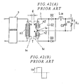
- a rectifier circuit 7 provided on the secondary side of a separable transformer T, and a circuit for supplying a load current I to a load 10 consisting of a variable resistance through a choke coil LCH, as shown in Fig. 39 (A).
- a high-frequency AC voltage by an inverter 3.
- the rectifier circuit 7, which is a well-known full-wave rectifier circuit provides a center tap 5e on a secondary winding n2 of the transformer T, connects both ends of the secondary winding n2 to respective anodes of diodes D2, D3, and connects cathodes of both the diodes D2, D3 to each other.
- a serial circuit consisting of the choke coil LCH and the load 10, a capacitor C3 being connected parallel to the load 10.
- the axis of abscissa is for a load current I, the axis of ordinate on the left side for a load voltage V0, and the axis of the ordinate on the right side for a load power P, the curve V indicating the load voltage and the curve P indicating the load power.
- the transformer T has a configuration as shown in Fig. 40, in which the primary winding n1 is separately wrapped at two leg portions of the U-type primary core 5c, the secondary winding n2 is separately wrapped at two leg portions of the U-type secondary core 5d, and the center tap 5e is provided at the middle point of the secondary winding n2.
- the inductance value when viewed from the primary winding terminals A ⁇ A' of the transformer T is 112 ⁇ H
- the inductance value when viewed from the secondary winding terminals B ⁇ B' is 42 ⁇ H
- the mutual inductance value between the primary winding n1 and the secondary winding n2 is 91 ⁇ H.
- a matching capacitor is connected in parallel or series with the secondary winding n2 of the transformer T in order to offset an effect due to the leakage inductance of the transformer T, thereby increasing an effective power taken from the primary side to secondary side of the transformer T (improving a power factor by load matching).
- Providing such a matching capacitor causes a power transmission efficiency to be significantly improved for a certain load, thereby allowing the system to be miniaturized. Therefore, the matching capacitor is an important component in commercially applying a non-contact electrical power transmission system.
- the axis of abscissa is for the load current I
- the axis of ordinate on the left side for the load voltage V0 and the axis of the ordinate on the right side for the load power P
- the curve V indicating the load voltage
- the curve P indicating the load power.
- a value obtained with (varying range of load voltage V0)/(varying range of load current) is referred to as the voltage change rate.
- a method of making constant (stabilizing) the load voltage for a plural kinds of loads identical in load voltage and different in power that is, different in load current
- a method such as that of providing a feedback control circuit which detects a load voltage at the secondary side of the transformer T, compares said detected voltage with a reference value to amplify an error, transmits in non-contact fashion the error-amplified signal to the primary side of the transformer T, and controls the amplitude, frequency and duty of the high-frequency AC voltage supplied to the primary winding n1 of the transformer T, or that of providing an independent stabilizing source circuit at the secondary side of the transformer T and connecting the circuit to the load.
- the relationship of the output terminal voltage and load power with the load current is such that as shown in Fig. 36, the load power P is substantially proportional to the load current I, and the output terminal voltage V0 can be stabilized in a light load through full load region B, but it becomes rapidly larger in a no load through minute load region A.
- a matching capacitor for load matching is often provided on the secondary winding side. It will be assumed that providing the matching capacitor causes the unique above-mentioned voltage rise different from the switching source due to normal contact coupling at the time of no-load/minute load.
- dummy loads such as dummy resistances are connected parallel to the output terminal to generate a loss at all time to control, but in this method, a power loss at the dummy voltage becomes several watts or more, and the circuit size becomes large or the cost increases in order to control the efficiency decrease and temperature rise.
- the non-contact electrical power transmission system comprises a transformer having a primary winding and a secondary winding separable and detachable therebetween, a capacitor connected parallel to the secondary winding of the above-mentioned transformer, and an output terminal provided on the above-mentioned secondary winding side and connected with a load, and supplies a high-frequency AC voltage to the above-mentioned primary winding to flow a high-frequency current to the above-mentioned primary winding, and generates an induced voltage on the secondary winding by the electromagnetic induction action, whereby a power is supplied to the load connected to the above-mentioned output terminal.
- This system is configured such that a voltage supplied to the above-mentioned load is substantially constant, a flowing current varies, and a power is supplied to a different load, and in the system, taking as a first condition a fact that at the time of maximum load, the time of the reversal of the voltage polarity in the above-mentioned primary winding substantially coincides with the time of the oscillating voltage of the above-mentioned capacitor reaching its maximum or minimum value, and as a second condition a fact that at the time of minimum load, the time of the reversal of the voltage polarity in the above-mentioned primary winding substantially coincides with the time of the oscillating voltage of the above-mentioned capacitor completing one cycle, the above-mentioned capacitor is set so that its capacity value satisfies simultaneously the above-mentioned first and second conditions, thereby making constant the load voltage in a minimum through maximum load current range.
- the above-mentioned configuration allows the load voltage to be made constant in a wide load current range with an inexpensive circuit configuration without providing the feedback control circuit, that is, without making complex the circuit. Therefore, a substantially-constant load voltage can be supplied to a load whose load current largely varies or to plural kinds of loads whose load voltages are constant and load currents are different from each other.
- This system may be configured such that in the system, instead of the above-mentioned second condition, taking as a second condition a fact that at the time of minimum load, the timing of the reversal of the voltage polarity in the above-mentioned primary winding substantially coincides with the timing of the oscillating voltage of the above-mentioned capacitor starting oscillation, and at the same time, the timing of the reversal of the voltage polarity in the above-mentioned primary winding substantially coincides with the timing of the oscillating voltage of the above-mentioned capacitor completing one cycle, the above-mentioned capacitor is set so that its capacity value satisfies simultaneously the above-mentioned first and second conditions.
- This allows the output voltage to be made constant for a load current equal to or less than the maximum value in the above-mentioned load current range.
- This system in which a dummy load for flowing a current equal to or more than the above-mentioned minimum value even in the load current region smaller than the minimum value in the above-mentioned load current range is connected between the above-mentioned output terminals, can flow a current equal to or more than the above-mentioned minimum value even in the load current region smaller than the minimum value in the above-mentioned load current range.
- This system includes a drive circuit for supplying the above-mentioned high-frequency AC voltage to the above-mentioned primary winding, and in the above-mentioned drive circuit, the frequency of the above-mentioned high-frequency AC voltage changes automatically so that when the above-mentioned load current is within the above-mentioned load current range, the voltage supplied to a load is made constant. Hence, the load voltage can be made constant in a wide load current range.
- This system includes a drive circuit for supplying the above-mentioned high-frequency AC voltage to the above-mentioned primary winding, the above-mentioned drive circuit consisting of a resonance-type inverter.
- the above-mentioned drive circuit may be a partial resonance-type inverter having a resonating capacitor which is connected parallel to the above-mentioned primary winding and develops a resonance between the capacitor and the above-mentioned primary winding. This allows the load voltage to be made constant in a wide load current range while maintaining a soft switching.
- the above-mentioned drive circuit may be the one which includes a voltage resonance circuit by the above-mentioned primary winding and by a resonating capacitor connected parallel to the above-mentioned primary winding, and the voltage waveform of the above-mentioned high-frequency AC voltage exhibits a sinusoidal waveform.
- the above-mentioned drive circuit should be such that in a period when the on-time of a switching element switched in said drive circuit is constant, and a partial resonance develops, and at the same time, in at least one period of either the rising period or the falling period of the voltage waveform of the above-mentioned high-frequency AC voltage, at least one of either the time of said period or the voltage waveform of said period varies corresponding to the load current. This allows the load voltage to be made constant in a wide load current range while maintaining a soft switching.
- the above-mentioned inverter can employ a half-bridge type one or a push-pull type one. This causes the utilizing efficiency of the transformer core to be improved.
- the above-mentioned inverter may be a self-excited one which includes a feedback winding and an auxiliary winding each magnetically coupled to the primary winding of the above-mentioned transformer, a voltage-drive type switching element given an input voltage the control end through the feedback winding, and a charging/discharging circuit connected between both ends of the auxiliary winding for controlling the above-mentioned input voltage, and when a charge voltage due to an induced voltage of the auxiliary winding reaches a specified value, lowers the above-mentioned input voltage to turn off the above-mentioned switching element.
- the non-contact electrical power transmission system comprises an inverter circuit including a transformer having a structure of the primary winding and the secondary winding whose voltage is induced by the primary winding being separable and detachable therebetween, a first capacitor connected to the above-mentioned secondary winding side for being matched with a load, a rectifier circuit for rectifying a voltage induced in the above-mentioned secondary winding, a current-smoothing reactor for smoothing an output current of the above-mentioned rectifier circuit, and an output terminal supplied with a smoothed output by the above-mentioned reactor and connected with the load, and in the system, an inductance value of the above-mentioned reactor is selected so that when the magnitude of the above-mentioned load is made changed, the load current value at the time when the output voltage of when the magnitude of the above-mentioned rectifier circuit varies from a discontinuous condition to a continuous condition is made smaller, whereby the rise of the inverter circuit including
- a dummy load capable of flowing at all time a load current value at the time when the output current of the above-mentioned rectifier circuit varies from a discontinuous condition to a continuous condition may be connected to the output terminal.
- a second capacitor is connected parallel to the above-mentioned current-smoothing reactor, and an electrostatic capacity value of the above-mentioned second capacitor is set so that the AC voltage component of the voltage at the input side of the above-mentioned current-smoothing reactor exhibits a sinusoidal waveform. This allows the rise of the output terminal voltage to be controlled even at the time of no-load/minute load and a loss to be made lower even a case of connecting a dummy load.
- the electrostatic capacity value of the above-mentioned second capacitor is set so that when the load is increase gradually from no-load, the amplitude of the AC voltage component of the voltage at the input side of the above-mentioned current-smoothing reactor becomes equal to that of the output terminal voltage.
- the electrostatic capacity value of the above-mentioned second capacitor may be set so that when the load is increased gradually from no-load, the load current value at the time when the zero period in which the output current of the above-mentioned rectifier circuit is zero dissipates becomes smallest.
- a resonance frequency determined by the inductance value of the above-mentioned current-smoothing reactor and by the electrostatic capacity value of the second capacitor is equal to two times the frequency of the voltage applied to the primary winding.
- a resonance frequency determined by the electrostatic capacity value of the above-mentioned first capacitor and by the leakage inductance value converted to the secondary side the separable and detachable transformer may be equal to two times the frequency of the voltage applied to the primary winding.
- the above-mentioned secondary winding includes a center tap
- the rectifier circuit consists of two diodes, and connects one end of the above-mentioned each diode in series and in opposite direction to each other to both output ends (not to the center tap) of the above-mentioned secondary winding, thereby configuring a full-wave rectifier circuit interconnecting the other ends of the above-mentioned each diode.
- the load current value at the time when the output current of the above-mentioned rectifier circuit varies from a discontinuous condition to a continuous condition is made smaller, thereby controlling the rise of the output terminal voltage at the time of the load being no-load or minute load.
- Fig. 1 shows a circuit of the non-contact electrical power transmission system in accordance with an embodiment of the present invention.
- This non-contact electrical power transmission system has a configuration equal to the prior art one of the above-mentioned Fig. 42 (A), except for the setting of circuit constants, such that a rectifier circuit 7 for full-wave rectifying the output of a secondary winding n2 is provided on the secondary side of a separable transformer T, a circuit in series with a choke coil LCH and a load 10 consisting of a resistance is connected between the output ends of the rectifier circuit 7, and a capacitor C3 is connected parallel to the load 10.
- the secondary winding n2 of the transformer T is connected parallel with a matching capacitor C2.
- a primary winding n1 of the transformer T is supplied with a high-frequency AC voltage from an inverter 3 as a drive circuit.
- the transformer T has the same configuration as the prior art one described in Fig. 40.
- the inventor of the present invention discovered a fact that in measuring output characteristics such as a load voltage (output voltage) ⁇ load current characteristics and a load power ⁇ load current characteristics as shown in the above-mentioned Fig. 44 by changing variously the resistance value of the load 10 in the circuit shown in Fig. 42 (A), there is a region in which changing the capacity value of the capacitor C2 causes the output characteristics to exhibit various shaped, but by selecting appropriately the capacity value of the capacitor C2, a fluctuation of the load voltage (output voltage) with respect to a change of the load current can be made small (That is, there is a region in which the above-mentioned voltage change rate can be made small). Examples of such output characteristics are shown in respective Fig. 2 and Fig. 3.
- Fig. 2 and Fig. 3 each is a load voltage ⁇ load current characteristic graph, and also an output characteristic graph obtained by applying a square-wave-shaped high-frequency AC voltage with a maximum amplitude 70 V and a frequency approximately 97 kHz as shown in the above-mentioned Fig. 39 (B) to the primary winding n1 and by changing variously the resistance value of the load 10 taking the inductance value of the choke coil LCH as 100 ⁇ H, the capacity value of the capacitor C3 connected parallel to the load 10 as 100 ⁇ F, and the gap g between the primary side core 5c of the transformer T and the secondary side core 5d as 2 mm in the circuit shown in Fig. 42 (A).
- the axis of abscissa is for a load current
- the axis of ordinate on the left side for load voltage V0
- the axis of the ordinate on the right side for a load power P
- the curve V indicating the load voltage
- the curve P indicating the load power
- Fig. 2 and Fig. 3 there exists a load current range having a relatively small above-mentioned voltage change rate (changed width of load voltage V0/changed width of load current I) compared to the output characteristics of the above-mentioned Fig. 44.
- the maximum value (hereinafter referred to the maximum load current value) of the load current I in the load current range having a relatively small above-mentioned voltage change rate is expressed as an Imax
- the minimum value (hereinafter referred to the minimum load current value) of the load current I in said load current range as an Imin.
- the voltage change rate in a load current range from the minimum load current value Imin to the maximum load current value Imax is about 0.6/A. It will be understood that on the contrary, in the load voltage ⁇ load current characteristics of the above-mentioned Fig. 44, the voltage change rate in the load current range of the load current values 1 through 4 A is about 2.5 V/A, so that the load voltage ⁇ load current characteristics shown in Fig. 2 and Fig. 3 becomes sufficiently small in the voltage change rate compared to the load voltage ⁇ load current characteristics shown in Fig. 44. That is, the load voltage V0 is substantially stable in the load current range from the minimum load current value Imin to the maximum load current value Imax, thereby allowing the load voltage in the load current range to be made constant.
- Fig. 4 through Fig. 6 are graphs illustrating the operation waveform of each part in the equivalent circuit converted to the secondary side of the circuit of Fig. 42 (A) shown in Fig.
- the polarity reverse time (for example, times t1, t3) of the voltage E1S across the primary winding n1 as shown in Fig. 4 (a) substantially coincides with the time (times t1, t3) when the voltage VC2 across the capacitor C2 reaches the maximum and minimum values as shown in Fig. 4 (c).
- the voltage VC2 across the capacitor C2 starts from an approximate zero volt condition the charging of the capacitor C2, reaches the maximum value or the minimum value, starts the discharging of the capacitor C2, then returns back to the approximate zero volt condition, the polarity of the voltage E1S across the primary winding n1 (and the induced voltage E3S converted to the secondary side) reverses.
- the time of the polarity reverse of the voltage E1S across the primary winding n1 substantially coincides with the time when the discharging of the capacitor C2 completes in the charging/discharging of the capacitor C2, in other words, the time when the oscillation waveform of the voltage VC2 across the capacitor C2 completes one cycle.
- One-cycle completion means that the voltage VC2 across the capacitor C2 starts the oscillation, passes through the maximum value or the minimum value once, then returns again back to the approximate zero volt condition
- the operation waveform at the time when the magnitude of the load current I exhibits an arbitrary current value from the above-mentioned minimum load current value Imin to the maximum load current value Imax is an intermediate waveform between the waveform satisfying the condition in which the load current I exhibits the maximum load current value Imax and the waveform satisfying the condition in which the load current I exhibits the minimum load current value Imin.
- making constant the load voltage V0 is usually required for a region from a no-load time to a full-load time of a load device, so that it is desirable to have output characteristics as shown in Fig. 3 and to set the load current range at a range from the minimum load current value Imin to the maximum load current value Imax.
- the load voltage V0 can be made constant (stabilized) in a load current range from the minimum load current value Imin at the time of approximately no-load to the maximum load current value Imax as shown in Fig. 3.
- the inductance value of the leakage inductance L02 can be obtained by shorting between the winding terminals A ⁇ A' of the primary winding n1 and measuring the inductance value when viewed from the winding terminals B ⁇ B' of the secondary winding n2 in the configuration of the transformer T shown in Fig. 40.
- the output characteristics as shown in Fig. 3 can be obtained by setting circuit constants to satisfy the relationship of these formulas (1) through (3).
- the current IC2 of the capacitor C2 is not necessarily required to become approximately zero.
- the non-contact electrical power transmission system of this embodiment which is the same as the prior art configuration shown in Fig. 42 (A), has features in that taking as a first condition a fact that the time of the polarity reversal of the voltage E1S across the primary winding n1 of the transformer T substantially coincides with the time when the voltage VC2 across the capacitor C2 reaches the maximum and minimum values to specify the maximum load current value Imax of the maximum value in a load current range supplied to the load 10 in the circuit shown in Fig.
- the capacity value of the capacitor C2 is set to satisfy simultaneously the above-mentioned first and second conditions.
- the load voltage V0 can be made constant in a wide load current I, so that a substantially ⁇ constant load voltage V0 can be supplied to a load 10 largely changing in the load current I, or to various kinds of loads 10 in which the load voltages V0 are constant and the load currents I different from each other.
- Fig. 7 (A) shows a circuit of the non-contact electrical power transmission system in accordance with this embodiment.
- This non-contact electrical power transmission system has the same configuration as that of the first embodiment shown Fig. 1, and however, different from it in that the circuit uses a rechargeable battery as a load 10 connected between output terminals and is utilized as charging device for recharging the rechargeable battery.
- Components similar to those in the first embodiment are accorded the same references to omit their explanation.
- a constant-voltage load such as the rechargeable battery as a load 10
- the characteristics expressing the relationship between the capacity value of the matching capacitor C2 connected parallel to the secondary winding n2 and the load current I has a trend as shown in Fig. 8.
- the capacity value of the capacitor C2 when the load current I reaches a maximum value by changing the capacity value of the capacitor C2 is referred to as C2max.
- C2max the capacity value of the capacitor C2 when the load current I reaches a maximum value by changing the capacity value of the capacitor C2
- the capacity value of the capacitor C2 is made C2max, the maximum value of the load current (charge current) I can be obtained, while when the capacity value of the capacitor C2 is made shifted from C2max, the charge current I is decreased.
- changing the frequency (hereinafter referred to as the drive frequency) of the high-frequency AC voltage with a square wave supplied to the primary winding n1 as shown in Fig. 7 (B) causes the load current characteristics for the capacity value of the capacitor C2 to vary in a fashion, for example, shown with lines 1, 2, 3, 4 in Fig. 9, in which the drive frequency becomes lower in the order of 1, 2, and 3, followed by 4.
- Changing the drive frequency causes C2max to vary, and the higher the drive frequency is made, the lower the capacity value of C2max becomes. Therefore, as shown in Fig.
- the above-mentioned characteristics are those in case where the load voltage V0 is constant, the characteristics indicate that when such a load that an increase in load current I causes a decrease in load voltage V0 is used such as the resistant load of the load 10 as shown in Fig. 42, or the load provided with a smoothing capacitor, changing the drive frequency corresponding to a change of the load current I allows the load voltage V0 to be kept approximately constant value.
- the capacity value of the capacitor C2 is set according to the self-inductance of the primary winding n1, the self-inductance of the secondary winding n2, the mutual inductance between the primary winding n1 and the secondary winding n2, and the highest drive frequency. Therefore, the drive frequency is required to be automatically changed so as to correspond to the load current I.
- the magnitude of the voltage amplitude of the primary winding n1 is proportional to the load current I. Therefore, as a method of making constant (stabilizing) the load voltage (output voltage), there is devised a method of controlling the voltage amplitude of the input voltage (high-frequency AC voltage) of the primary winding n1 depending on the change of the load voltage V0 due to the change of load current I. As a method embodying it, there is a method with which, in a circuit as shown in Fig. 12 (A), the voltage waveform of the high-frequency AC voltage supplied to the primary winding n1 of the transformer T is made changed from the square-wave voltage waveform as shown in Fig.
- changing the voltage waveform means changing the inclination of the high-frequency AC voltage at its rising time and falling time.
- the input voltage of the primary winding n1 is made the trapezoidal wave shape to make smaller the equivalent voltage amplitude applied to the primary winding n1, thereby restraining the rise of the load voltage V0, while as the load current I becomes larger, the input voltage is made close to the square wave shape to make larger the equivalent voltage amplitude applied to the primary winding n1, thereby restraining the drop of the load voltage V0, whereby the load voltage V0 can be made constant (stabilized) in a wide load current I range. Only the equivalent voltage amplitude is required to be changed without changing the maximum amplitude, so that the waveform to be changed from the square wave is not limited to the trapezoidal wave. This commercial application requires means of changing automatically the waveform corresponding to the load current I, thereby controlling automatically the equivalent voltage amplitude of the high-frequency AC voltage applied to the primary winding n1.
- a non-contact electrical power transmission system capable of changing automatically the drive frequency and the voltage waveform of the high-frequency AC voltage corresponding to the load current I.
- Fig. 15 is an example in which a drive circuit 3 for supplying the high-frequency AC voltage to the primary winding n1 of the transformer T is configured by a half-bridge type inverter. Components similar to those in the first embodiment are accorded the same references.
- This non-contact electrical power transmission system comprises the transformer T whose primary winding n1 and secondary winding n2 are separable therebetween, a DC power source E, a drive circuit 3 consisting of the half-bridge type inverter for converting the voltage of the DC power source E connected between the output terminals of the DC power source E to the high-frequency AC voltage to supply the voltage to the primary winding n1 of the transformer T, the matching capacitor C2 connected parallel to the secondary winding n2 of the transformer T, the rectifier circuit 7 for rectifying the voltage generated in the secondary winding n2 of the transformer T and supplying the rectified voltage to the load 10, the choke coil LCH inserted between the rectifier circuit 7 and the load 10, and the capacitor C3 connected parallel to the load 10.
- the drive circuit 3 which is a half-bridge type inverter as mentioned above, in which a serial circuit of a pair of capacitors Ca, Cb and a serial circuit of switching elements S1, S2 consisting of a pair of power MOSFETs are connected parallel to each other between the output terminals of the DC power source E, and in which the primary winding n1 of the transformer T is inserted between the connecting point of both the capacitors Ca, Cb and the connecting point of both the switching elements S1, S2.
- circulating diodes DS1, DS2 connected reversely parallel to the switching elements S1, S2 consist of body diodes of the MOSFETs of each switching elements S1, S2, these diodes DS1, DS2 may be provided separately.
- the DC power source E is obtained , for example, by smoothing a commercial power source.
- This drive circuit 3 applies the high-frequency AC voltage with a square wave to the primary winding n1 of the transformer T in a manner such that the switching elements S1, S2 are turned alternately on and off by a control circuit (not shown).
- the rectifier circuit 7 is a well-known full-wave rectifier circuit, in which the center tap 5e is provided on the secondary winding n2 of the transformer T, both ends of the secondary winding n2 are connected to the anodes of the diodes D2, D3, respectively, and the cathodes of both the diodes D2, D3 are connected to each other.
- the above-mentioned choke coil LCH is inserted between the mutual connecting point of the diodes D2, D3 and one end of the load 10, and the center tap 5e is connected to the other end of the load 10.
- the choke coil LCH is required to make continuous and smooth the load current I
- the capacitor C3 is not necessarily required to be provided.
- Fig. 16 shows a circuit of the non-contact electrical power transmission system having the capacitor C1 connected parallel to the primary winding n1 of the transformer T in the circuit configuration shown in the above-mentioned Fig. 15.
- the capacity value of the capacitor C1 is made relatively large to utilize a resonance of an inductance component L1 of the primary winding n1 and the like therewith.
- the entire circuit is an object of the resonance when the load 10 side is viewed from the primary winding n1, the resonance condition varies according to the primary winding n1, the secondary winding n2, the mutual inductance, the capacitor C2 on the secondary side, and the load 10.
- the capacitor C1 is not necessarily required to be connected parallel to the primary winding n1, but may be connected to provide an equivalent circuit.
- the capacitor may be provided parallel to the switching element S1 and the switching element S2.
- Fig. 17 shows the operation waveform of each part of the circuit of Fig.
- the dead time in which both the switching elements S1, S2 become off as shown in Fig. 17 (g)
- (h) during alternately turning on/off of the switching elements S1, S2 cause the voltage VL across the primary winding n1 together with the inductance component L1 of the primary winding n1 and the like to generate a resonance voltage by the resonance circuit of the capacitor C1 during the dead time as shown in Fig. 17 (a), whereby the voltage varies until it reaches the power source voltage or GND level, and when the power source voltage or GND level is reached, the voltage is clamped by the circulating diodes DS1, DS2.
- the present invention has features in that the waveform of the voltage VL across the primary winding n1 is made a trapezoidal wave shape as shown in Fig. 17 (a) by utilizing the capacitor C1 having a relatively large capacity value to make large the resonance frequency by the above-mentioned inductance component L1 and the like with the capacitor C1.
- selecting a specific capacity value as the capacity value of the capacitor C1 in order to obtain a resonance voltage forming the rising and falling (both in the dead time period) of the trapezoidal wave causes both the rising and falling time to become relatively long in at no-load, and both the rising and falling time to become relatively short at full-load (provided that the on-time period of the switching elements S1, S2 is constant in a load range), whereby the drive frequency becomes low at no-load, and becomes high at full-load, so that it works in a manner to stabilize the load voltage V0.
- the waveform of the voltage VL across the primary winding n1 is changed from the trapezoidal wave to the square wave, whereby the equivalent voltage amplitude of the voltage applied to the primary winding n1 at no-load becomes lower than for the square wave, thereby restraining the rise of the load voltage V0.
- the resonance determining the rising time and falling time of the voltage VL across the primary winding n1 is not established only the capacitor C1 and the inductance component L1 as mentioned above, but by the capacitor C1, the primary winding n1 when the load side is viewed from the inductance component L1 side, the secondary winding n2, the mutual inductance, and the circuit including the capacitor C2 on the secondary side and the load 10. Further, the resonance is also affected by rectifying-smoothing system. Therefore, it will be assumed that the condition change of the load 10 (for example, where the load 10 is a resistance, change of resistance value) acts mutually with the circuit system, whereby the change is reflected as change of the resonance frequency, with the result that the rising and falling time and the waveform are automatically changed.
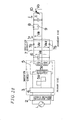
- Fig. 18 shows a circuit of the non-contact electrical power transmission system in accordance with this embodiment. While the drive circuit 3 in the circuit described in the second embodiment shown in Fig. 17 is a separately-excited half-bridge type inverter, the drive circuit 3 in the non-contact electrical power transmission system of this embodiment consists of a self-excited partial oscillation converter. In this embodiment, there is not required to provide separately a control circuit including an oscillation circuit for turning on/off voltage-drive type switching elements S 1 and S2 such as MOSFETs.
- the configuration of the transformer T, and the configuration of the rectifier circuit 7 for rectifying the output of the secondary winding n2 thereof are similar to those of the second embodiment.
- the serial circuit of a pair of capacitors Ca, Cb, and the serial circuit of the switching elements S1, S2 consisting of a pair of power MOSFETs are connected parallel to each other to the serial circuit of the DC power source E and a switch SW; the primary winding n1 of the transformer T is inserted between the connecting point of both the capacitors Ca, Cb and the connecting point of both the switching elements S1, S2; and the capacitor C1 is connected parallel to the primary winding n1.
- a circulating diode (not shown) consisting of the body diodes of MOSFETs is connected reversely parallel to each switching elements S1, S2.
- the DC power source E is obtained, for example, by rectifying/smoothing a commercial power source.
- This drive circuit 3 includes two feedback windings nf1, nf2 and two auxiliary windings ns1, ns2 magnetically coupled to the primary winding n1 of the transformer T, respectively.
- the serial circuit of resistances R7, R8 and capacitors C5, C6 is connected across respective switching elements S1, S2; and the serial circuit of the above-mentioned feedback windings nf1, nf2 and resistances R1, R4 is inserted between the connecting point of the resistances R7, R8 with the capacitors C5, C6, and the control terminals of the switching elements S1, S2.
- Applied to the control terminals of the switching elements S1, S2 is an input voltage through the above-mentioned feedback windings nf1, nf2.
- the charging/discharging circuit connected across the auxiliary windings ns1 consists of resistances R2, R3, R10, diodes D11, D12, D16, D21, capacitors C7, C8, and a transistor Tr1, the diode D21 and the transistor Tr1 configuring a discharging circuit.
- the charging/discharging circuit connected across the auxiliary windings ns2 consists of resistances R5, R6, R11, diodes D13, D14, D17, D22, capacitors C9, C10, and a transistor Tr2, the diode D22 and the transistor Tr2 configuring a discharging circuit.
- Closing the switch SW causes the capacitors C5, C6 to be charged through the resistances R7, R8.
- the voltage of the capacitors C5, C6 is applied to the gate of the switching elements S1, S2, so that when the voltage of either of the capacitors C5, C6 reaches a threshold value of the switching elements S1, S2, for example, when the voltage of the capacitor C5 reaches a threshold value of the switching element S1, the switching elements S1 is turned on to cause the current IL to begin to flow through the primary winding n1.
- an induced voltage develops in the feedback winding nf1 in the direction in which the switching element S1 continues to be on, whereby the switching element S1 maintains a stable on-condition.
- This induced voltage is superimposed on the electric potential of the capacitor C6.
- the on-condition of the switching element S1 can be sufficiently maintained even only by the induced voltage of the feedback winding nf1.
- an induced voltage develops also in the auxiliary windings ns1.
- the auxiliary windings ns1 is connected with the above-mentioned charging/discharging circuit, so that when the induced voltage develops in the auxiliary windings ns1, the capacitor C7 is charged through the diode D11 and the resistance R2, and at the same time, the capacitor C8 connected between the base and emitter of the transistor Tr1 is charged through the diode D15.
- the transistor Tr1 is turned on, the gate voltage of the switching elements S1 lowers, so that the switching elements S1 is turned off.
- the switching elements S1 When the switching elements S1 is turned off, the current IL having flowed through the primary winding n1 is communicated to the capacitor C1 so as to maintain the current, and in such a condition, there begins a free oscillation (for convenience, referred to as the resonance) of the capacitor C1 with a circuit when the load side is viewed from the inductance component LI side of the primary winding n1.
- the resonance begins, and in a short time, the voltage VD1 across the switching elements S1 becomes the power source voltage VE, the voltage VD1 is clamped through a circulating diode (not shown) consisting of the body diode of the switching elements S2 to the power source voltage VE.
- the polarity reversal of the voltage VL and the current direction change of the current IL causes a reverse voltage to be induced in the feedback winding nf1 and the auxiliary winding ns1, thereby maintaining the off-condition of the switching elements S1, and at the same time, the reversely-induced voltage of the auxiliary winding ns1 pulls through the diode D12 and the resistance R3 out the electric charge of the capacitor C7 to make approximately zero. At this time, the electric charge of the capacitor C8 is also gradually discharged through the resistance R10. Simultaneously with the operation, a positive induced voltage develops in the feedback winding nf2 and the auxiliary winding ns2.
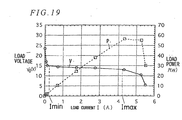
- Fig. 19 a result obtained by changing the resistance value of the load 10, and measuring the load voltage ⁇ load current characteristics and the load power ⁇ load current characteristics. It will be understood in Fig. 19 that the voltage change rate in a load current range from the minimum load current value Imin to the maximum load current value Imax of the load current I is on the order of 0.4 V/A, which is improved further than the voltage change rate (0.6 V/A) in the output characteristics of Fig. 3 described in the first embodiment.
- FIG. 20 An example of the waveform at the time of a load current close to no-load involved in this improvement, and an example of the waveform at the time of a load current close to full-load are shown in Fig, 20 and Fig. 21, respectively.
- (a) indicates the voltage VL across the primary winding n1;
- (b) the voltage VC2 across the capacitor C2;
- (c) the load current I flowing through the load 10;
- (d) the load voltage V0.
- the voltage waveform of the primary winding n1 is a trapezoidal waveform with a frequency approximately 70 kHz, while at full-load shown in Fig. 21, the voltage waveform of the primary winding n1 is a trapezoidal waveform with a frequency approximately 80 kHz.
- the frequency varies automatically on the order of 10 kHz, and the waveform also can automatically embody a change of a shape such as an inclination at the rising time and the falling time.
- the on-time of each switching elements S1, S2 at this time has been approximately 4 ⁇ seconds constantly.
- the dead time is provided as mentioned above, and there can be discovered in a manner of trial and error a combination of circuit constants which can change automatically the rising time and falling time of the resonance voltage (either of the time being a time period from the resonance starting time to the time when the resonance voltage is clamped to the source voltage or ground potential) utilizing resonance during the dead time, or the voltage waveform according to the load. More specifically, measuring the waveform at a load close to no-load and at full-load can discover a combination of constants appropriately varying with respect to period or waveform.
- the load voltage V0 becomes large in a current region in which the load current I is smaller than the minimum load current value Imin. Since such a state is often found actually, it is sufficient to connect previously a resistance and the like as a dummy load to an output terminal (load connecting terminal) so that a load current equivalent to the minimum load current value Imin can flow.
- the basic configuration of the non-contact electrical power transmission system according to this embodiment is substantially the same as that of the first and second embodiments, and the system has features in that as shown in Fig. 22, it uses a push-pull type inverter as a drive circuit 3 for supplying the high-frequency AC voltage to the primary winding n1 of the separable transformer T.
- the basic configuration of the non-contact electrical power transmission system according to this embodiment is substantially the same as that of the first and second embodiments, and the system has features in that as shown in Fig. 23, there are provided diodes Df1, Df2 connected in series to the switching elements S1, S2 and reversely to circulating diodes DS1, DS2 so that the voltage of the primary winding n1 is not clamped at ground level, thereby operating the resonance voltage as the waveform of sinusoidal wave.
- the present invention relates to a non-contact electrical power transmission system using a separable transformer having inevitably a low-degree of magnetic coupling and a large leakage inductance for power transmission
- the present invention can also be applied to a case where a fixed transformer used with the degree of magnetic coupling made lowered is used for power transmission, whereby the load voltage can be stabilized in a wide load current change range without providing a feedback control circuit, and even when providing a feedback control circuit, the number of additional parts and an additional cost can be reduced.
- Fig. 24 shows a configuration of a non-contact electrical power transmission system.
- the system comprises a AC power source 1, an input rectifying/smoothing circuit 2 for rectifying/smoothing the AC power source 1, an inverter circuit 3, a first capacitor 6 connected parallel to a secondary winding 5b for matching the load on the secondary winding 5b side, a rectifier circuit 7 for full-wave rectifying an induced voltage of the secondary winding 5b, a current matching reactor 8 for smoothing an output current I7 of the rectifier circuit 7, a variable resistance 10 being a load, and a capacitor 11 connected parallel to the variable resistance 10.
- the inverter circuit 3 consists of a power converting section 4 for converting the output of the input rectifying/smoothing circuit 2 to a high-frequency power, and a transformer 5 into which the high-frequency power is inputted from the power converting section 4.
- the transformer 5 consists of a primary winding 5a, and a secondary winding 5b having a center tap 5e and for receiving a power whose voltage is induced by the primary winding 5a.
- the variable resistance 10 is connected to the output terminal of the current matching reactor 8 and to the center tap 5e of the secondary winding 5b.
- the primary winding 5a and the secondary winding 5b configure the separable/detachable transformer 5.
- the rectifier circuit 7 consists of diodes 7a, 7b, and is configured by connecting one ends of the diodes 7a, 7b serially and mutually in an opposite direction with both output ends opposite to the center tap 5e of the secondary winding 5b, and by connecting the other ends of the diodes 7a, 7b to each other.
- the capacitor 11 not only includes a capacitor for smoothing the output terminal voltage supplied to the variable resistance 10 and a noise controlling capacitor, but also includes a capacity due to elements or substrates and a capacity of an input part inside the variable resistance 10.
- Fig. 25 shows a configuration of the separable/detachable transformer 5, in which the primary side is formed by wrapping the primary winding 5a on a core 5c consisting of a magnetic substance, while the secondary side is formed by wrapping the secondary winding 5b on a core 5d and by being provided with the center tap 5e, both the primary side and the secondary side being oppositely arranged through a gap G.
- the characteristics of the output terminal voltage V0 and the load power P with respect to the load current I supplied to the variable resistance 10 when using such a separable/detachable transformer 5 is shown as in Fig.
- the induced voltage V6 of the secondary winding 5b and the pre-rectification voltages V61, V62 are of a similar AC waveform with sinusoidal wave shape in both the no-load ⁇ minute load region A and the light load ⁇ full load region B.
- the rectifier circuit output current I7 exhibits a discontinuous condition in which a current flowing time and a no-current flowing time are alternately repeated in rectifier circuit in the no-load ⁇ minute load region A, while it exhibits a continuous condition in which a current flows at all time in the light load ⁇ full load region B.
- the reactor input part voltage V8 exhibits a waveform on which a sinusoidal wave-shaped AC voltage is superimposed in the light load ⁇ full load region B, while in the no-load ⁇ minute load region A, a ringing is superimposed to cause the waveform to fluctuate during zero period in which no rectifier circuit output current 17 flows.
- the output terminal voltage V0 at this time becomes larger in the no-load ⁇ minute load region A than in the light load ⁇ full load region B, so that it can be predicted that the rapid increase of the output terminal voltage V0 in the no-load ⁇ minute load region A is caused by the rectifier circuit output current I7 and the reactor input part voltage V8.
- the rectifier circuit output current I7 exhibits a continuous condition with respect to all load currents I in which the rectified waveform of the pre-rectification voltage V61 (or V62) appears as the reactor input part voltage V8 as it is.
- the reactor input part voltage V8 exhibits a waveform in which a sinusoidal-wave shaped AC voltage is superimposed as an AC voltage component on an amplitude V0' of the output terminal voltage V0, an amplitude V1' of the sinusoidal-wave shaped AC voltage being equal to the amplitude V0' of the output terminal voltage V0. Therefore, it will be assumed that if each waveform satisfies these features, a rise of the output terminal voltage V0 can be prevented at the load current I at that time.
- the waveform of the reactor input part voltage V8 does not exhibit the rectified waveform of the pre-rectification voltage V61 (or V62), so that a ringing is superimposed to cause the waveform to fluctuate during the zero period when no rectifier circuit output current I7 flows.
- the increase in the discontinuity of the rectifier circuit output current I7 corresponds to a fact that the amplitude V1' of the sinusoidal wave-shaped AC voltage superimposed on the amplitude V0' of the output terminal voltage V0 becomes decreased compared to the amplitude V0' .
- the output terminal voltage V0 increases to near the peak voltage of the pre-rectification voltage V61 (or V62), and the amplitude V1' approaches zero.
- V61 pre-rectification voltage
- V1' the amplitude V1' approaches zero.
- the load current I when the rectifier circuit output current I7 begins to vary from the discontinuous condition to the discontinuous condition is made as small as possible, and a dummy load is used combinedly.
- the dummy load may be substituted by the self-loss of already-used circuit parts in some cases.
- Fig. 27 shows characteristics of the load current I and the output terminal voltage V0 when the inductance value L8 of the current smoothing reactor 8 is made changed to a large, medium, and small value.
- Making large the inductance value L8 of the current smoothing reactor 8 causes the load current I when the rectifier circuit output current I7 begins to vary from the discontinuous condition to the continuous condition to become smaller, thereby allowing the range in which the rise of the output terminal voltage V0 is restrained to be widened. This also allows the loss of the dummy load connected parallel to the output terminal to be made small in order to provide a commercial application.
- Fig. 28 shows the circuit in which a second capacitor 9 is connected parallel to the current smoothing reactor 8 of the circuit shown in Fig. 24. Selecting appropriately the electrostatic capacity of the second capacitor 9 can widen the range in which the rise of the output terminal voltage V0 is restrained even in the no-load ⁇ minute-load region A compared to Fig. 36, as shown in Fig. 29.
- the induced voltage V6 of the secondary winding 5b, the voltage (pre-rectification voltage) V61 between one end of the secondary winding 5b and the center tap 5e, the voltage (pre-rectification voltage) V62 between the other end of the secondary winding 5b and the center tap 5e, the voltage (reactor input part voltage) V8 between the input terminal of the current smoothing reactor 8 and the center tap 5e, and the rectifier circuit output current I7 (the current flowing into the current smoothing reactor 8 and the second capacitor 9) are shown in Fig. 30 with respect to their waveform.
- the induced voltage V6 of the secondary winding 5b, the pre-rectification voltage V61, and the pre-rectification voltage V62 exhibit a sinusoidal wave-shaped AC voltage waveform.
- Selecting appropriately the electrostatic capacity of the second capacitor 9 causes the zero period of the rectifier circuit output current I7 to be shortened, the reactor input part voltage V8 to approach the reactor input part voltage V8 shown in Fig. 26 (b), the rectifier circuit output current I7 to exhibit a continuous condition in some cases, and the reactor input part voltage V8 to exhibit a waveform on which a sinusoidal wave-shaped AC voltage waveform is superimposed, thereby allowing a rise of the output terminal voltage V0 to be restrained.
- the induced voltage V6 of the secondary winding 5b is also a sinusoidal wave-shaped AC voltage, and has the same frequency as the frequency f of the voltage applied to the primary winding 5a, while the sinusoidal wave-shaped AC voltage of the reactor input part voltage V8 has a frequency of two times the frequency f.
- the formula (4) can be used to predict the electrostatic capacity value C9 of the second capacitor 9 capable of shortening the zero period of the rectifier circuit output current I7 to a largest extent, and restraining the rise of the output terminal voltage V0 down to a load current I smaller than that before improvement in the no-load ⁇ minute-load region A.
- Fig. 31 is an equivalent circuit obtained by converting the circuit shown in Fig. 28 to the secondary side of the transformer 5.
- the inductance value measured from the two terminals except for the center tap of the secondary winding 5b with the two terminals of the primary winding 5a of the transformer 5 shorted out is the leakage inductance value L5 (not shown) converted to the secondary side of the transformer 5.
- the leakage inductance value L5 is equivalent to a sum of inductance values L5i of two leakage inductances 5i shown in Fig. 31.
- the secondary winding 5b is equivalent to the serial circuit of voltage sources 12a, 12b and the two leakage inductances 5i; the voltage sources 12a, 12b generate the pre-rectification voltages V61, V62; and the outlet of the center tap of the secondary winding 5b becomes the connecting middle point of the voltage sources 12a, 12b.
- each values are set so that the leakage inductance value L5 converted to the secondary side, the electrostatic capacity value C6 of the first capacitor 6 connected parallel to the secondary winding 5b, and the frequency f of the voltage applied to the primary winding 5a satisfy the following relationship, and the configuration is made to include the capacitor 9.
- Fig. 32 is an embodiment in which the inverter circuit 3 on the primary side is made a half-bridge configuration, and a resonance capacitor 34 is connected parallel to the primary winding 5a to provide a partial-resonance type inverter.
- the power source is expressed as a DC power source 31 by omitting the AC power source 1 and the input rectifying/smoothing circuit 2.
- the inverter circuit 3 comprises the DC power source 31, the serial circuit of capacitors 32, 33 and the serial circuit of switching elements 35, 36 connected parallel to the DC power source 31, diodes 37,38 connected parallel to the switching elements 35, 36, respectively, and the parallel circuit of the primary winding 5a and the resonance capacitor 34 connected to the connecting point of the capacitors 32, 33 and to the connecting point of the switching elements 35, 36.
- the voltage waveform applied to the primary winding 5a exhibits a trapezoidal wave shape, the switching loss of the switching elements 35, 36 can be reduced, and the noise also be reduced, so that not only the secondary side but also the primary side can be made small in size. Therefore, there can be provided a small-size non-contact electrical power transmission system capable of stabilizing the output terminal voltage V0 in a wide load range from near no-load to full-load.
- a rise of the output terminal voltage V0 occurs near the no-load region as shown in Fig. 29.
- a dummy load such as a resistance, a constant-voltage element, a light-emitting element and a display element any of which can flow the load current I at all time in the point E of Fig. 29.
- the load current I becomes considerably small when the output terminal voltage V0 rises, so that common small-size electronic parts can be used, thereby preventing the size from becoming large.
- Fig. 34 is an example in which a constant-voltage element 15 as a dummy load is connected to the output terminal. This not only allows the output terminal voltage V0 to be stabilized, but also constrains the output terminal voltage V0 to a constant value even if a transient abnormal voltage develops on the secondary side due to some cause.
- the present invention relates to a non-contact electrical power transmission system utilizing an electromagnetic induction, and when this system is applied to a detachable plug and an outlet, an exposed metallic contact can be made unnecessary, thereby eliminating an electric shock and a poor contact.
- this system is suitable for a power supply source in the places relating to water such as a bathroom, a washroom, a kitchen and a toilet.
- Fig. 37 shows an example in which this system is applied to a bathroom outlet system.
- Fig. 38 (A) shows a condition in which the plug and outlet of the system have not been connected;
- Fig. 38 (B) shows a condition in which the plug and outlet of the system have been connected.
- a wall 54 dividing the room into a bathroom interior 52 including a bathtub 51 and a bathroom exterior 53 is provided with a power feed section 55 to which this system is applied.
- the primary side as an outlet is arranged to be buried in the wall, and the primary coil 5a is given a high-frequency AC from a commercial power source to generate a high-frequency flux.
- the primary coil 5a is opened through an insulator to the bathroom interior 52, the opening serving as an outlet 55a.
- An inverter 3 is contained in the outlet 55a.
- a load apparatus 56 As an example of a load apparatus 56, a motor-driven brush for cleaning the bathroom is shown.
- the load apparatus 56 has through a cord 57 a plug 55b containing a waterproof-secondary coil 5b integrally with an electrical insulator, in which apparatus, the plug 55b is attached to or removed from the outlet 55a to receive or stop power transmission.
- the operation voltage of the load apparatus 56 is set at, for example, about 12 V
- Applying the present invention allows a voltage to be maintained at about 12 V in a range from a heavy load when rotating a motor to a no load or a light load (such as for LED lamp display).
- the voltage drop becomes large proportional to the load to cause the performance of an apparatus not to be exhibited, or the apparatus to be damaged.
- Monitoring the voltage of a load apparatus to perform an active control by PMW control and the like in order to stabilize the output voltage causes the size and cost of an outlet and a plug to be increased, while applying the present invention causes an active control to be eliminated, and even when using combinedly the active control, only a few parts to be added, thereby reducing a burden of size and cost.
- it is necessary to provide sufficiently an electric shock prevention so that it suffices to fill the circuit or coil contained the outlet and plug with a potting material and to insulate the coil and core with an insulating bobbin.
- the application of the present invention is suitable for a power feed section provided on the garden, park, road and the like subject directly to rain outdoors, for a power fed section for transmitting a power from inside the room or vehicle through a window glass to outdoors, and for a power feed section under water.
- No problem with a poor contact causes this system to be suitable for the power transmission in a dusty outdoors or a salty place such as seaside.
- power transmission can be performed through an insulator, so that a power transmission can be performed from outside to a tightly-closed space containing bacteria, hazardous material and the like.
- Making the coupling of the primary coil and the secondary coil to exhibit an axially-symmetric shape allows a power transmission to be performed at a rotatable area such as a robot arm.
- the present invention is not limited to the configurations of the above-mentioned embodiments, and may be embodied in various modifications, so that the present invention includes configurations, which are equivalent in circuit and mechanism and easily replaceable, such as output rectifying systems, waveforms of voltage applied to the primary winding, primary side circuit systems, and kinds of loads.
Abstract
Description
100 µF, a gap g between a
Claims (9)
- A non-contact electrical power transmission system comprising:when the magnitude of said load (10) is made changed, an inductance value of said reactor (8) is selected so to make small a load current value when the output current of said rectifier circuit (2) is changed from a discontinuous condition to a continuous condition, thereby restraining a rise of said output voltage when said load is no-load or minute-load.an inverter circuit (3) including a transformer (5) having a structure in which a primary winding (5a) and a secondary winding (5b) on which a voltage is induced by said primary winding (5a) are separable and detachable;a first capacitor (6) connected to said secondary winding side for matching a load;a rectifier circuit (2) for rectifying a voltage induced in said secondary winding;a current smoothing reactor (8) for smoothing an output current of said rectifier circuit (7); andan output terminal to which a smoothed output by said reactor (8) is supplied and a load (10) is connected; characterized in that
- A non-contact electrical power transmission system as set forth in claim 1, characterized in that a dummy load capable of flowing at all time a load current value when the output current of said rectifier circuit (2) is changed from a discontinuous condition to a continuous condition is connected to the output terminal.
- A non-contact electrical power transmission system as set forth in claim 1, characterized in that a second capacitor (9) is connected parallel to said current smoothing reactor (8), and the electrostatic capacity of said second capacitor (9) is set so that the AC voltage component of the voltage on the input side of said current smoothing reactor (8) becomes a sinusoidal shape.
- A non-contact electrical power transmission system as set forth in claim 3, characterized in that when a load (10) is made increased gradually from no-load, the electrostatic capacity of said second capacitor (9) is set so that the amplitude of the AC voltage component of the voltage on the input side of said current smoothing reactor (8) becomes equal to the amplitude of the output terminal voltage.
- A non-contact electrical power transmission system as set forth in claim 3, characterized in that when a load is made increased gradually from no-load, the electrostatic capacity of said second capacitor (9) is set so that the load current value when the zero period of the output current of said rectifier circuit (7) being zero dissipates becomes a minimum.
- A non-contact electrical power transmission system as set forth in claim 3, characterized in that a resonance frequency determined by the inductance value of said current-smoothing reactor (8) and the electrostatic capacity of said second capacitor (9) is equal to two times the frequency of the voltage applied to the primary winding (5a).
- A non-contact electrical power transmission system as set forth in claim 1, characterized in that a resonance frequency determined by the electrostatic capacity of said first capacitor (6) and the leakage inductance value converted to the secondary side of the separable/detachable transformer (5) is equal to two times the frequency of the voltage applied to the primary winding (5a).
- A non-contact electrical power transmission system as set forth in claim 1, characterized in that a full-wave rectifier circuit (7) is configured such that said secondary winding (5b) includes a center tap (5e), the rectifier circuit (7) consists of two diodes (7a, 7b), and one ends of said diodes (7a, 7b) are connected in series to both output terminals being not the center tap (5e) of said secondary winding (5b) and mutually in opposite direction thereto, while the other ends of said diodes (7a, 7b) are mutually connected to each other.
- A non-contact electrical power transmission system as set forth in claim 1, characterized in that when making large the inductance value of said current-smoothing reactor causes the magnitude of a load to be changed, the load current value when the output current of said rectifier circuit (7) is changed from a discontinuous condition to a continuous condition is made small, thereby restraining a rise of the output terminal voltage when the load is no-load or minute-load.
Applications Claiming Priority (5)
| Application Number | Priority Date | Filing Date | Title |
|---|---|---|---|
| JP2000048351 | 2000-02-24 | ||
| JP2000048351A JP4258939B2 (en) | 2000-02-24 | 2000-02-24 | Non-contact power transmission device |
| JP2000256643A JP4240783B2 (en) | 2000-08-28 | 2000-08-28 | Non-contact power transmission device |
| JP2000256643 | 2000-08-28 | ||
| EP01104150A EP1130752B1 (en) | 2000-02-24 | 2001-02-21 | Non-contact electrical power transmission system having function of making load voltage constant |
Related Parent Applications (2)
| Application Number | Title | Priority Date | Filing Date |
|---|---|---|---|
| EP01104150.6 Division | 2001-02-21 | ||
| EP01104150A Division EP1130752B1 (en) | 2000-02-24 | 2001-02-21 | Non-contact electrical power transmission system having function of making load voltage constant |
Publications (3)
| Publication Number | Publication Date |
|---|---|
| EP1469584A2 true EP1469584A2 (en) | 2004-10-20 |
| EP1469584A3 EP1469584A3 (en) | 2005-01-05 |
| EP1469584B1 EP1469584B1 (en) | 2009-08-05 |
Family
ID=26586051
Family Applications (2)
| Application Number | Title | Priority Date | Filing Date |
|---|---|---|---|
| EP04014754A Expired - Lifetime EP1469584B1 (en) | 2000-02-24 | 2001-02-21 | Non-contact electrical power transmission system having function of making load voltage constant |
| EP01104150A Expired - Lifetime EP1130752B1 (en) | 2000-02-24 | 2001-02-21 | Non-contact electrical power transmission system having function of making load voltage constant |
Family Applications After (1)
| Application Number | Title | Priority Date | Filing Date |
|---|---|---|---|
| EP01104150A Expired - Lifetime EP1130752B1 (en) | 2000-02-24 | 2001-02-21 | Non-contact electrical power transmission system having function of making load voltage constant |
Country Status (4)
| Country | Link |
|---|---|
| US (1) | US6504732B2 (en) |
| EP (2) | EP1469584B1 (en) |
| AT (2) | ATE438948T1 (en) |
| DE (2) | DE60110660T2 (en) |
Cited By (1)
| Publication number | Priority date | Publication date | Assignee | Title |
|---|---|---|---|---|
| CN111478560A (en) * | 2020-04-30 | 2020-07-31 | 陕西亚成微电子股份有限公司 | Control method and circuit for gallium nitride power tube |
Families Citing this family (56)
| Publication number | Priority date | Publication date | Assignee | Title |
|---|---|---|---|---|
| US7212414B2 (en) * | 1999-06-21 | 2007-05-01 | Access Business Group International, Llc | Adaptive inductive power supply |
| US7522878B2 (en) | 1999-06-21 | 2009-04-21 | Access Business Group International Llc | Adaptive inductive power supply with communication |
| GB2377822A (en) * | 2001-06-15 | 2003-01-22 | Marconi Applied Technologies | Transformer arrangement for delivering low voltage power to a high voltage device |
| US6617737B1 (en) * | 2002-06-13 | 2003-09-09 | One World Technologies, Inc. | Apparatus and method of powering light source |
| KR20060016072A (en) * | 2002-12-31 | 2006-02-21 | 아포지 테크놀로지, 인크. | Adaptive resonant switching power system |
| CN1781168B (en) * | 2003-05-02 | 2011-06-29 | 乔治·阿兰·林普金 | Apparatus for supplying energy to a load and a related system |
| KR20040106763A (en) * | 2003-06-11 | 2004-12-18 | 위니아만도 주식회사 | Contactless power supply |
| KR100573769B1 (en) * | 2003-12-10 | 2006-04-25 | 삼성전자주식회사 | Non-contact feeder system |
| WO2005104343A1 (en) * | 2004-04-21 | 2005-11-03 | Mitsubishi Denki Kabushiki Kaisha | Power supply apparatus |
| US7489526B2 (en) * | 2004-08-20 | 2009-02-10 | Analog Devices, Inc. | Power and information signal transfer using micro-transformers |
| US7558080B2 (en) * | 2004-08-20 | 2009-07-07 | Analog Devices, Inc. | Power converter system |
| WO2006022365A1 (en) * | 2004-08-27 | 2006-03-02 | Hokushin Denki Co., Ltd. | Non-contact power transmission device |
| US7218539B2 (en) * | 2005-03-22 | 2007-05-15 | Delphi Technologies, Inc. | Technique for increasing power capability of a DC-to-AC converter |
| US7197268B2 (en) * | 2005-07-01 | 2007-03-27 | Xerox Corporation | Current measurement circuit for transformer with high frequency output |
| EP1816659A1 (en) * | 2006-02-02 | 2007-08-08 | Efbe Elektrogeräte GmbH | Electric household appliance system |
| US20080068132A1 (en) * | 2006-05-16 | 2008-03-20 | Georges Kayanakis | Contactless radiofrequency device featuring several antennas and related antenna selection circuit |
| US8369109B2 (en) * | 2006-11-09 | 2013-02-05 | Osram Gesellschaft Mit Beschrankter Haftung | Self-oscillating bipolar transistor DC/AC/DC converter using a pulse forming timer |
| JP2010086943A (en) | 2008-09-04 | 2010-04-15 | Toshiba Lighting & Technology Corp | Led lighting device and illumination fixture |
| US8076620B2 (en) * | 2008-11-07 | 2011-12-13 | Lance P. Johnson | Anti-oxidation food preparation device |
| CN101814838B (en) * | 2009-02-19 | 2013-02-27 | 艾默生网络能源系统北美公司 | Control method and device of power converter of resonance topological circuit |
| WO2011021485A1 (en) * | 2009-08-19 | 2011-02-24 | 株式会社安川電機 | Output filter and electric motor drive system provided therewith |
| US8174233B2 (en) * | 2009-10-08 | 2012-05-08 | Etymotic Research, Inc. | Magnetically coupled battery charging system |
| US8174234B2 (en) * | 2009-10-08 | 2012-05-08 | Etymotic Research, Inc. | Magnetically coupled battery charging system |
| US8022775B2 (en) * | 2009-10-08 | 2011-09-20 | Etymotic Research, Inc. | Systems and methods for maintaining a drive signal to a resonant circuit at a resonant frequency |
| US8460816B2 (en) * | 2009-10-08 | 2013-06-11 | Etymotic Research, Inc. | Rechargeable battery assemblies and methods of constructing rechargeable battery assemblies |
| US8237402B2 (en) * | 2009-10-08 | 2012-08-07 | Etymotic Research, Inc. | Magnetically coupled battery charging system |
| CN102610379A (en) * | 2011-01-25 | 2012-07-25 | 深圳市摩西尔电子有限公司 | Connector and signal transmission method |
| CN103299526B (en) * | 2011-02-01 | 2015-08-26 | 富士电机株式会社 | Resonant switching power equipment |
| KR101322843B1 (en) | 2011-05-17 | 2013-10-28 | 삼성전자주식회사 | Method and apparatus for rx system for wireless power transmission using rx system |
| DE102011118564A1 (en) * | 2011-11-15 | 2013-05-16 | Grossenbacher System Ag | Contactless power supply and signal transmission through cladding element for building parts |
| US10129935B2 (en) | 2011-12-29 | 2018-11-13 | Arcelik Anonim Sirketi | Wireless kitchen appliance operated on an induction heating cooker |
| EP2798909B1 (en) | 2011-12-29 | 2017-04-05 | Arçelik Anonim Sirketi | Wireless kitchen appliance operated on induction heating cooker |
| KR101349557B1 (en) | 2012-03-19 | 2014-01-10 | 엘지이노텍 주식회사 | Apparatus for receiving wireless power and method for deliveringng wireless power |
| EP2884626A4 (en) * | 2012-08-07 | 2016-07-20 | Lequio Power Technology Corp | Lighting system, power supply device, and light fixture |
| US9293997B2 (en) | 2013-03-14 | 2016-03-22 | Analog Devices Global | Isolated error amplifier for isolated power supplies |
| US9160289B2 (en) * | 2013-05-10 | 2015-10-13 | Raytheon Company | Broadband power amplifier having high efficiency |
| GB2520037B (en) * | 2013-11-07 | 2021-08-11 | Greengage Lighting Ltd | Power distribution |
| US10536309B2 (en) | 2014-09-15 | 2020-01-14 | Analog Devices, Inc. | Demodulation of on-off-key modulated signals in signal isolator systems |
| US9660848B2 (en) | 2014-09-15 | 2017-05-23 | Analog Devices Global | Methods and structures to generate on/off keyed carrier signals for signal isolators |
| US10270630B2 (en) | 2014-09-15 | 2019-04-23 | Analog Devices, Inc. | Demodulation of on-off-key modulated signals in signal isolator systems |
| CN104331550B (en) * | 2014-10-28 | 2017-10-31 | 中国南方电网有限责任公司电网技术研究中心 | Smoothing reactor broadband electromagnetical transient analysis equivalent circuit based on transmission line structure |
| US9998301B2 (en) | 2014-11-03 | 2018-06-12 | Analog Devices, Inc. | Signal isolator system with protection for common mode transients |
| CN104410278B (en) * | 2014-12-26 | 2017-02-22 | 阳光电源股份有限公司 | DCDC converter |
| CA3008661A1 (en) * | 2015-12-22 | 2017-06-29 | Thermatool Corp. | High frequency power supply system with closely regulated output for heating a workpiece |
| DE102016002465B4 (en) | 2016-03-01 | 2020-11-05 | Audi Ag | Regulator device and method for setting a battery current of a battery of a motor vehicle |
| US10141980B2 (en) * | 2017-04-26 | 2018-11-27 | Minebea Mitsumi Inc. | Wireless power transmission system, and communication and protection methods for the same |
| JP6724897B2 (en) * | 2017-12-28 | 2020-07-15 | 株式会社豊田中央研究所 | Non-contact power transfer device, battery pack using the same, power grid system, and power transfer method |
| US10610068B2 (en) | 2018-01-06 | 2020-04-07 | Kohler Co. | Toilet seat and hinge |
| CN110752580B (en) * | 2018-07-23 | 2021-06-01 | 中国科学院沈阳自动化研究所 | Connection box power supply system and method for submarine observation network |
| CN109713803A (en) * | 2019-03-21 | 2019-05-03 | 杭州电子科技大学 | A kind of water surface robot wireless charging device |
| CN110336384A (en) * | 2019-05-05 | 2019-10-15 | 杭州电子科技大学 | A kind of wireless closed-loop voltage-stabilizing controller based on inductively coupled power transfer |
| EP3920373A4 (en) * | 2019-08-07 | 2023-01-25 | Huawei Digital Power Technologies Co., Ltd. | Wireless charging device, and method and system for position detection |
| US11387678B2 (en) * | 2019-09-27 | 2022-07-12 | Apple Inc. | Stacked resonant structures for wireless power systems |
| CN111208370B (en) * | 2020-01-16 | 2022-06-17 | 宁波市江北九方和荣电气有限公司 | Full-automatic test device for capacitor aging test |
| CN111722152B (en) * | 2020-06-29 | 2023-04-28 | 成都工百利自动化设备有限公司 | Transformer winding deformation monitoring method and monitoring system |
| CN115020094B (en) * | 2022-08-08 | 2022-12-09 | 山东大学 | Low-cost high-frequency current signal sensor |
Citations (8)
| Publication number | Priority date | Publication date | Assignee | Title |
|---|---|---|---|---|
| JPH0556641A (en) * | 1991-08-28 | 1993-03-05 | Fuji Electric Co Ltd | Switching power supply |
| JPH06217542A (en) * | 1993-01-14 | 1994-08-05 | Origin Electric Co Ltd | Resonant dc-dc converter |
| DE4344071A1 (en) * | 1993-12-23 | 1995-07-06 | Josef Femboeck | Energy and/or data transmission device |
| JPH0880042A (en) * | 1994-06-27 | 1996-03-22 | Matsushita Electric Works Ltd | Power device |
| JPH099621A (en) * | 1995-06-23 | 1997-01-10 | Canon Inc | Voltage resonance-type power supply apparatus |
| JPH09121534A (en) * | 1995-10-26 | 1997-05-06 | Matsushita Electric Ind Co Ltd | Dc-dc converter |
| US5954985A (en) * | 1995-12-08 | 1999-09-21 | Thermatool Corp. | Matching apparatus for connecting high frequency solid state electrical power |
| US6108216A (en) * | 1999-02-23 | 2000-08-22 | Matsushita Electric Works, Ltd. | Non-contact electrical power transmission system |
Family Cites Families (7)
| Publication number | Priority date | Publication date | Assignee | Title |
|---|---|---|---|---|
| GB2170663B (en) * | 1985-02-02 | 1989-06-14 | Brian Ernest Attwood | Harmonic-resonant power supply |
| US5376912A (en) * | 1992-03-12 | 1994-12-27 | Casagrande; Serge | Combined transformer and inductor |
| JPH06169569A (en) * | 1992-09-14 | 1994-06-14 | Origin Electric Co Ltd | High power factor ac/dc converter |
| DE4403707A1 (en) * | 1994-02-07 | 1995-08-10 | Leica Mikroskopie & Syst | Regulated power supply unit with an electronic transformer |
| CN1052586C (en) * | 1996-06-24 | 2000-05-17 | Tdk株式会社 | Switching power unit |
| JPH1198837A (en) * | 1997-09-24 | 1999-04-09 | Sansha Electric Mfg Co Ltd | Dc power source apparatus |
| US6301128B1 (en) * | 2000-02-09 | 2001-10-09 | Delta Electronics, Inc. | Contactless electrical energy transmission system |
-
2001
- 2001-02-21 EP EP04014754A patent/EP1469584B1/en not_active Expired - Lifetime
- 2001-02-21 DE DE60110660T patent/DE60110660T2/en not_active Expired - Lifetime
- 2001-02-21 AT AT04014754T patent/ATE438948T1/en not_active IP Right Cessation
- 2001-02-21 AT AT01104150T patent/ATE295624T1/en not_active IP Right Cessation
- 2001-02-21 DE DE60139512T patent/DE60139512D1/en not_active Expired - Lifetime
- 2001-02-21 EP EP01104150A patent/EP1130752B1/en not_active Expired - Lifetime
- 2001-02-26 US US09/793,154 patent/US6504732B2/en not_active Expired - Fee Related
Patent Citations (8)
| Publication number | Priority date | Publication date | Assignee | Title |
|---|---|---|---|---|
| JPH0556641A (en) * | 1991-08-28 | 1993-03-05 | Fuji Electric Co Ltd | Switching power supply |
| JPH06217542A (en) * | 1993-01-14 | 1994-08-05 | Origin Electric Co Ltd | Resonant dc-dc converter |
| DE4344071A1 (en) * | 1993-12-23 | 1995-07-06 | Josef Femboeck | Energy and/or data transmission device |
| JPH0880042A (en) * | 1994-06-27 | 1996-03-22 | Matsushita Electric Works Ltd | Power device |
| JPH099621A (en) * | 1995-06-23 | 1997-01-10 | Canon Inc | Voltage resonance-type power supply apparatus |
| JPH09121534A (en) * | 1995-10-26 | 1997-05-06 | Matsushita Electric Ind Co Ltd | Dc-dc converter |
| US5954985A (en) * | 1995-12-08 | 1999-09-21 | Thermatool Corp. | Matching apparatus for connecting high frequency solid state electrical power |
| US6108216A (en) * | 1999-02-23 | 2000-08-22 | Matsushita Electric Works, Ltd. | Non-contact electrical power transmission system |
Non-Patent Citations (5)
| Title |
|---|
| PATENT ABSTRACTS OF JAPAN vol. 0173, no. 71 (E-1396), 13 July 1993 (1993-07-13) & JP 5 056641 A (FUJI ELECTRIC CO LTD), 5 March 1993 (1993-03-05) * |
| PATENT ABSTRACTS OF JAPAN vol. 0185, no. 86 (E-1627), 9 November 1994 (1994-11-09) & JP 6 217542 A (ORIGIN ELECTRIC CO LTD), 5 August 1994 (1994-08-05) * |
| PATENT ABSTRACTS OF JAPAN vol. 1996, no. 07, 31 July 1996 (1996-07-31) & JP 8 080042 A (MATSUSHITA ELECTRIC WORKS LTD), 22 March 1996 (1996-03-22) * |
| PATENT ABSTRACTS OF JAPAN vol. 1997, no. 05, 30 May 1997 (1997-05-30) & JP 9 009621 A (CANON INC), 10 January 1997 (1997-01-10) * |
| PATENT ABSTRACTS OF JAPAN vol. 1997, no. 09, 30 September 1997 (1997-09-30) & JP 09 121534 A (MATSUSHITA ELECTRIC IND CO LTD), 6 May 1997 (1997-05-06) * |
Cited By (2)
| Publication number | Priority date | Publication date | Assignee | Title |
|---|---|---|---|---|
| CN111478560A (en) * | 2020-04-30 | 2020-07-31 | 陕西亚成微电子股份有限公司 | Control method and circuit for gallium nitride power tube |
| CN111478560B (en) * | 2020-04-30 | 2022-09-06 | 陕西亚成微电子股份有限公司 | Control method and circuit for gallium nitride power tube |
Also Published As
| Publication number | Publication date |
|---|---|
| EP1130752A2 (en) | 2001-09-05 |
| EP1469584B1 (en) | 2009-08-05 |
| ATE295624T1 (en) | 2005-05-15 |
| DE60110660T2 (en) | 2005-10-06 |
| US6504732B2 (en) | 2003-01-07 |
| EP1130752A3 (en) | 2003-07-23 |
| DE60139512D1 (en) | 2009-09-17 |
| EP1469584A3 (en) | 2005-01-05 |
| EP1130752B1 (en) | 2005-05-11 |
| US20010017781A1 (en) | 2001-08-30 |
| DE60110660D1 (en) | 2005-06-16 |
| ATE438948T1 (en) | 2009-08-15 |
Similar Documents
| Publication | Publication Date | Title |
|---|---|---|
| EP1130752B1 (en) | Non-contact electrical power transmission system having function of making load voltage constant | |
| JP4135299B2 (en) | Non-contact power transmission device | |
| KR100660403B1 (en) | Switching Power Supply | |
| EP1193851B1 (en) | Switching power supply device having series capacitance | |
| JP5253304B2 (en) | Circuit and method for responding to a current derived from a voltage across the input of an energy transfer element | |
| US6366480B2 (en) | Switching power supply apparatus | |
| EP0851566A2 (en) | Half-bridge zero-voltage-switched PWM flyback DC/DC converter | |
| JP2001197740A (en) | Switching power supply | |
| WO2004088828A2 (en) | Phase-shifted resonant converter having reduced output ripple | |
| KR100572653B1 (en) | Current-resonant switching power supply | |
| US11251690B2 (en) | Systems, methods, and apparatus for dead-time control in resonant converters | |
| JP2000032750A (en) | Ac/dc converter | |
| JP4683364B2 (en) | Composite resonant switching power supply | |
| JP4352444B2 (en) | Resonant converter | |
| JP3591635B2 (en) | DC-DC converter | |
| JP4258939B2 (en) | Non-contact power transmission device | |
| WO2002025800A1 (en) | Switching mode power supply with high efficiency | |
| JP2002354798A (en) | Switching power supply | |
| KR100426605B1 (en) | Switching Power Supply Device Having Series Capacitance | |
| KR20000074998A (en) | Dc-dc converter | |
| JP2004328837A (en) | Switching power supply circuit and switching regulator comprising the same | |
| JP3194550B2 (en) | AC / DC converter | |
| JP2000295846A (en) | Inverter circuit and dc power supply | |
| JP2002272103A (en) | Switching power supply circuit | |
| JP2005094981A (en) | Switching power supply circuit |
Legal Events
| Date | Code | Title | Description |
|---|---|---|---|
| PUAI | Public reference made under article 153(3) epc to a published international application that has entered the european phase |
Free format text: ORIGINAL CODE: 0009012 |
|
| 17P | Request for examination filed |
Effective date: 20040623 |
|
| AC | Divisional application: reference to earlier application |
Ref document number: 1130752 Country of ref document: EP Kind code of ref document: P |
|
| AK | Designated contracting states |
Kind code of ref document: A2 Designated state(s): AT BE CH CY DE DK ES FI FR GB GR IE IT LI LU MC NL PT SE TR |
|
| PUAL | Search report despatched |
Free format text: ORIGINAL CODE: 0009013 |
|
| AK | Designated contracting states |
Kind code of ref document: A3 Designated state(s): AT BE CH CY DE DK ES FI FR GB GR IE IT LI LU MC NL PT SE TR |
|
| AKX | Designation fees paid |
Designated state(s): AT BE CH CY DE DK ES FI FR GB GR IE IT LI LU MC NL PT SE TR |
|
| 17Q | First examination report despatched |
Effective date: 20051006 |
|
| RAP1 | Party data changed (applicant data changed or rights of an application transferred) |
Owner name: PANASONIC ELECTRIC WORKS CO., LTD. |
|
| GRAP | Despatch of communication of intention to grant a patent |
Free format text: ORIGINAL CODE: EPIDOSNIGR1 |
|
| GRAS | Grant fee paid |
Free format text: ORIGINAL CODE: EPIDOSNIGR3 |
|
| GRAA | (expected) grant |
Free format text: ORIGINAL CODE: 0009210 |
|
| AC | Divisional application: reference to earlier application |
Ref document number: 1130752 Country of ref document: EP Kind code of ref document: P |
|
| AK | Designated contracting states |
Kind code of ref document: B1 Designated state(s): AT BE CH CY DE DK ES FI FR GB GR IE IT LI LU MC NL PT SE TR |
|
| REG | Reference to a national code |
Ref country code: GB Ref legal event code: FG4D |
|
| REG | Reference to a national code |
Ref country code: CH Ref legal event code: EP |
|
| REG | Reference to a national code |
Ref country code: IE Ref legal event code: FG4D |
|
| REF | Corresponds to: |
Ref document number: 60139512 Country of ref document: DE Date of ref document: 20090917 Kind code of ref document: P |
|
| PG25 | Lapsed in a contracting state [announced via postgrant information from national office to epo] |
Ref country code: AT Free format text: LAPSE BECAUSE OF FAILURE TO SUBMIT A TRANSLATION OF THE DESCRIPTION OR TO PAY THE FEE WITHIN THE PRESCRIBED TIME-LIMIT Effective date: 20090805 Ref country code: SE Free format text: LAPSE BECAUSE OF FAILURE TO SUBMIT A TRANSLATION OF THE DESCRIPTION OR TO PAY THE FEE WITHIN THE PRESCRIBED TIME-LIMIT Effective date: 20090805 Ref country code: ES Free format text: LAPSE BECAUSE OF FAILURE TO SUBMIT A TRANSLATION OF THE DESCRIPTION OR TO PAY THE FEE WITHIN THE PRESCRIBED TIME-LIMIT Effective date: 20091116 Ref country code: FI Free format text: LAPSE BECAUSE OF FAILURE TO SUBMIT A TRANSLATION OF THE DESCRIPTION OR TO PAY THE FEE WITHIN THE PRESCRIBED TIME-LIMIT Effective date: 20090805 |
|
| NLV1 | Nl: lapsed or annulled due to failure to fulfill the requirements of art. 29p and 29m of the patents act | ||
| PG25 | Lapsed in a contracting state [announced via postgrant information from national office to epo] |
Ref country code: NL Free format text: LAPSE BECAUSE OF FAILURE TO SUBMIT A TRANSLATION OF THE DESCRIPTION OR TO PAY THE FEE WITHIN THE PRESCRIBED TIME-LIMIT Effective date: 20090805 |
|
| PG25 | Lapsed in a contracting state [announced via postgrant information from national office to epo] |
Ref country code: PT Free format text: LAPSE BECAUSE OF FAILURE TO SUBMIT A TRANSLATION OF THE DESCRIPTION OR TO PAY THE FEE WITHIN THE PRESCRIBED TIME-LIMIT Effective date: 20091205 |
|
| PG25 | Lapsed in a contracting state [announced via postgrant information from national office to epo] |
Ref country code: DK Free format text: LAPSE BECAUSE OF FAILURE TO SUBMIT A TRANSLATION OF THE DESCRIPTION OR TO PAY THE FEE WITHIN THE PRESCRIBED TIME-LIMIT Effective date: 20090805 |
|
| PLBE | No opposition filed within time limit |
Free format text: ORIGINAL CODE: 0009261 |
|
| STAA | Information on the status of an ep patent application or granted ep patent |
Free format text: STATUS: NO OPPOSITION FILED WITHIN TIME LIMIT |
|
| PG25 | Lapsed in a contracting state [announced via postgrant information from national office to epo] |
Ref country code: BE Free format text: LAPSE BECAUSE OF FAILURE TO SUBMIT A TRANSLATION OF THE DESCRIPTION OR TO PAY THE FEE WITHIN THE PRESCRIBED TIME-LIMIT Effective date: 20090805 |
|
| 26N | No opposition filed |
Effective date: 20100507 |
|
| REG | Reference to a national code |
Ref country code: CH Ref legal event code: PL |
|
| GBPC | Gb: european patent ceased through non-payment of renewal fee |
Effective date: 20100221 |
|
| PG25 | Lapsed in a contracting state [announced via postgrant information from national office to epo] |
Ref country code: GR Free format text: LAPSE BECAUSE OF FAILURE TO SUBMIT A TRANSLATION OF THE DESCRIPTION OR TO PAY THE FEE WITHIN THE PRESCRIBED TIME-LIMIT Effective date: 20091106 Ref country code: CH Free format text: LAPSE BECAUSE OF NON-PAYMENT OF DUE FEES Effective date: 20100228 Ref country code: MC Free format text: LAPSE BECAUSE OF NON-PAYMENT OF DUE FEES Effective date: 20100301 Ref country code: LI Free format text: LAPSE BECAUSE OF NON-PAYMENT OF DUE FEES Effective date: 20100228 |
|
| PG25 | Lapsed in a contracting state [announced via postgrant information from national office to epo] |
Ref country code: IE Free format text: LAPSE BECAUSE OF NON-PAYMENT OF DUE FEES Effective date: 20100221 |
|
| PG25 | Lapsed in a contracting state [announced via postgrant information from national office to epo] |
Ref country code: GB Free format text: LAPSE BECAUSE OF NON-PAYMENT OF DUE FEES Effective date: 20100221 |
|
| PGFP | Annual fee paid to national office [announced via postgrant information from national office to epo] |
Ref country code: IT Payment date: 20110216 Year of fee payment: 11 Ref country code: FR Payment date: 20110218 Year of fee payment: 11 Ref country code: DE Payment date: 20110216 Year of fee payment: 11 |
|
| PG25 | Lapsed in a contracting state [announced via postgrant information from national office to epo] |
Ref country code: CY Free format text: LAPSE BECAUSE OF FAILURE TO SUBMIT A TRANSLATION OF THE DESCRIPTION OR TO PAY THE FEE WITHIN THE PRESCRIBED TIME-LIMIT Effective date: 20090805 |
|
| PG25 | Lapsed in a contracting state [announced via postgrant information from national office to epo] |
Ref country code: LU Free format text: LAPSE BECAUSE OF NON-PAYMENT OF DUE FEES Effective date: 20100221 |
|
| PG25 | Lapsed in a contracting state [announced via postgrant information from national office to epo] |
Ref country code: TR Free format text: LAPSE BECAUSE OF FAILURE TO SUBMIT A TRANSLATION OF THE DESCRIPTION OR TO PAY THE FEE WITHIN THE PRESCRIBED TIME-LIMIT Effective date: 20090805 |
|
| REG | Reference to a national code |
Ref country code: FR Ref legal event code: ST Effective date: 20121031 |
|
| PG25 | Lapsed in a contracting state [announced via postgrant information from national office to epo] |
Ref country code: IT Free format text: LAPSE BECAUSE OF NON-PAYMENT OF DUE FEES Effective date: 20120221 |
|
| REG | Reference to a national code |
Ref country code: DE Ref legal event code: R119 Ref document number: 60139512 Country of ref document: DE Effective date: 20120901 |
|
| PG25 | Lapsed in a contracting state [announced via postgrant information from national office to epo] |
Ref country code: FR Free format text: LAPSE BECAUSE OF NON-PAYMENT OF DUE FEES Effective date: 20120229 |
|
| PG25 | Lapsed in a contracting state [announced via postgrant information from national office to epo] |
Ref country code: DE Free format text: LAPSE BECAUSE OF NON-PAYMENT OF DUE FEES Effective date: 20120901 |