EP1469552A2 - Schlitzgekoppelte Radarantenne mit Strahlungsflächen - Google Patents
Schlitzgekoppelte Radarantenne mit Strahlungsflächen Download PDFInfo
- Publication number
- EP1469552A2 EP1469552A2 EP04003723A EP04003723A EP1469552A2 EP 1469552 A2 EP1469552 A2 EP 1469552A2 EP 04003723 A EP04003723 A EP 04003723A EP 04003723 A EP04003723 A EP 04003723A EP 1469552 A2 EP1469552 A2 EP 1469552A2
- Authority
- EP
- European Patent Office
- Prior art keywords
- housing
- radiation
- radiation surface
- ground surface
- radar antenna
- Prior art date
- Legal status (The legal status is an assumption and is not a legal conclusion. Google has not performed a legal analysis and makes no representation as to the accuracy of the status listed.)
- Withdrawn
Links
Images


Classifications
-
- H—ELECTRICITY
- H01—ELECTRIC ELEMENTS
- H01Q—ANTENNAS, i.e. RADIO AERIALS
- H01Q1/00—Details of, or arrangements associated with, antennas
- H01Q1/40—Radiating elements coated with or embedded in protective material
-
- H—ELECTRICITY
- H01—ELECTRIC ELEMENTS
- H01Q—ANTENNAS, i.e. RADIO AERIALS
- H01Q1/00—Details of, or arrangements associated with, antennas
- H01Q1/27—Adaptation for use in or on movable bodies
- H01Q1/32—Adaptation for use in or on road or rail vehicles
- H01Q1/3208—Adaptation for use in or on road or rail vehicles characterised by the application wherein the antenna is used
-
- H—ELECTRICITY
- H01—ELECTRIC ELEMENTS
- H01Q—ANTENNAS, i.e. RADIO AERIALS
- H01Q1/00—Details of, or arrangements associated with, antennas
- H01Q1/27—Adaptation for use in or on movable bodies
- H01Q1/32—Adaptation for use in or on road or rail vehicles
- H01Q1/3208—Adaptation for use in or on road or rail vehicles characterised by the application wherein the antenna is used
- H01Q1/3233—Adaptation for use in or on road or rail vehicles characterised by the application wherein the antenna is used particular used as part of a sensor or in a security system, e.g. for automotive radar, navigation systems
-
- H—ELECTRICITY
- H01—ELECTRIC ELEMENTS
- H01Q—ANTENNAS, i.e. RADIO AERIALS
- H01Q1/00—Details of, or arrangements associated with, antennas
- H01Q1/40—Radiating elements coated with or embedded in protective material
- H01Q1/405—Radome integrated radiating elements
-
- H—ELECTRICITY
- H01—ELECTRIC ELEMENTS
- H01Q—ANTENNAS, i.e. RADIO AERIALS
- H01Q9/00—Electrically-short antennas having dimensions not more than twice the operating wavelength and consisting of conductive active radiating elements
- H01Q9/04—Resonant antennas
- H01Q9/0407—Substantially flat resonant element parallel to ground plane, e.g. patch antenna
- H01Q9/045—Substantially flat resonant element parallel to ground plane, e.g. patch antenna with particular feeding means
- H01Q9/0457—Substantially flat resonant element parallel to ground plane, e.g. patch antenna with particular feeding means electromagnetically coupled to the feed line
Definitions
- the invention relates to a radar antenna for motor vehicle applications with at least one feed network on a first side of a high-frequency substrate, a metallic ground plane on a second side of the high-frequency substrate, which is opposite the feed network, and with at least one radiation surface, which has an assigned aperture in the metallic ground plane and above a dielectric arranged between the ground surface and the radiation surface is excited by the feed network to emit electromagnetic waves, and with a housing that accommodates the radar antenna.
- the invention also relates to a method for producing a radar sensor which has the features mentioned.
- radar sensors are generally used for surveillance in motor vehicles the vehicle environment used, applications such as Parking assistance, blind spot monitoring, accident anticipation (Pre-crash sensing), start / stop mode or driving mode with distance monitoring and / or regulation (cruise control support) come into question.
- Such an antenna has radiation areas (patches), which have an assigned aperture in a metallic Ground plane and over a between ground plane and Radiation area arranged dielectric of one Antenna feed network for radiation electromagnetic waves are excited.
- the aperture is usually designed as an elongated slot.
- Planar basic antenna elements can be used periodic arrangement of the basic antenna elements Build group spotlights, their dimensioning and geometric arrangement the direction of radiation, that is Field distribution in front of the antenna, determined.
- suitable phase-controlled excitation of phase-coupled resonators periodically arranged basic antenna elements can be a scanning of different spatial directions without change achieve the geometric alignment of the radar sensor (Principle of the phased array radar).
- planar antenna structures conventional antennas are in manufacture inexpensive and compact lightweight construction leave and easily with microstrip circuits in wide frequency ranges (approx. 100 MHz to 100 GHz) can be integrated.
- a broadband signal is desirable because the local resolution of reflecting objects, i.e. the smallest possible distance at which two separate objects as can be recognized separately, with increasing bandwidth improved.
- the Radar sensors are usually operated in pulsed mode since the Signal bandwidth with a shorter pulse width increased.
- the antenna areas are like this applied to a dielectric foam in front of or after applying the antenna surfaces to a solid Foam cures.
- the application of the antenna surfaces is typically done by sticking a film that carries several radiation surfaces (patches).
- the dimensions of the solid foam set the distance between the radiation surfaces from the apertures in the ground plane. A must the predetermined distance is observed as precisely as possible, because the distance affects the radiation. That's how it is Low radiation at comparatively small distances. while distances with a ratio of distance to radiated wavelength lambda between 0.1 and 0.2 the Favor radiation effect.
- That for carrying the antenna area in a certain Material used should be as low as possible Have dielectric constant when a broadband Radiation is desired. Because foams are low Have dielectric constant, they are in the known radar sensor used as a carrier material.
- the prefabricated sensor board with the antenna surfaces is in a protective plastic housing inserted.
- Another disadvantage is that the form and properties of the Foam material due to the constant temperature changes over the course of a vehicle's lifespan of several years change, so aging. In extreme cases, aging can Detach the radiation surfaces from the foam. In addition, a production of radar sensors is under Use of a foam as a carrier for one Large-scale production rather unsuitable.
- the object of the invention is the specification of a radar sensor does not have these disadvantages having.
- the task continues to be a process to manufacture a radar sensor indicate that the above avoids disadvantages mentioned.
- This task is the beginning of a radar sensor mentioned type solved in that the radiation area is firmly connected to the housing. This will be accordingly Task in a method of the type mentioned solved that the radiation surface firmly with the Housing is connected.
- a Reinforcement structure is arranged, the thickness of the Distance of the ground surface from the radiation surface defined.
- an air volume serving as a dielectric is defined by a recess in the reinforcing structure arranged between the radiation surface and the ground surface.
- the at least one Radiation area on one of the ground surface Side of the housing is arranged.
- the at least one Radiation area on one of the ground surfaces opposite, opposite side of the housing is arranged.
- This configuration has the advantage that the housing itself at least part of the distance from the Radiation area fills from the ground surface. This can the radar sensor should be kept flatter overall.
- the fixed Connection of the at least one radiation surface with the Housing is generated in that at least one prefabricated metallic radiation surface by a Hot stamping process is pressed onto the housing.
- Such a hot stamping process is technically high Placement accuracy of the radiation surfaces and with low technical effort feasible. Furthermore there is a very high quality of the connection of the Housing with the radiation surfaces because of the connection long-term stable and very firm.
- the hot stamping technology is a very inexpensive, reliable and reliable placement-accurate manufacturing method that is known that if the process parameters and the Plastic material even in demanding environmental environments as shows good results in the motor vehicle.
- the fixed connection of the thereby at least one radiation surface with the housing is generated that at least one prefabricated metallic radiation surface is glued to the housing.
- Adhesive processes are also technically easy to master, to carry out inexpensively and inexpensively.
- Etching processes also result in very high accuracy the arrangement of the radiation surfaces in connection with a high quality of connection. This also applies to that Cut out the patches with a laser.
- the number 10 in Figure 1 denotes the schematic General view of a radar sensor with a housing 12, the is completed by a lid 14.
- the dashed Lines 15 indicate the alignment or arrangement of individual radiation surfaces within the housing 12.
- the number 16 denotes a connection element via which the Radar sensor 10, for example, a supply voltage is supplied and / or via which the radar sensor 10 signals outputs to control units of a motor vehicle.
- the one with the Number 17 indicated arrow indicates the direction of Longitudinal axis of the motor vehicle.
- the orientation of the radar sensor 10 relative to the direction 17 of the longitudinal axis represents a typical installation position of the Radar sensor 10 in a motor vehicle application
- invention is not based on such relative orientation of the radar sensor 10 to the direction 17 the longitudinal axis of the motor vehicle is limited.
- FIG. 2 shows the radar sensor 10 of Figure 1 in Partial section, the inner shown in Figure 2 Structure of the radar sensor 10 is known per se.
- the figure 2 denotes the number 18 a feed network, which with the Connection element 16 from Figure 1 is connected and on the first side 20 of a high-frequency substrate 22 is arranged.
- a metallic ground surface 24 is on the second side 26 of the high-frequency substrate 22 is arranged.
- the radar sensor 10 also has at least one Radiation area 28 (patch) over an aperture 30 in the metallic ground plane 24 and over between the ground surface 24 and the radiation surface 28 Dielectric 32 from the feed network 18 for radiation electromagnetic waves is excited.
- the known Radar sensor is the radiation surface 28 on the Dielectric 32 is arranged and is therefore from the Dielectric 32 supported and carried.
- Dielectric 32 is usually realized as a hardening foam. The Use of a hardening foam as dielectric 32 brings with it the disadvantages mentioned at the outset.
- the radiation surface 28 is not a foam 32nd supported as a dielectric, but is rather firmly with connected to the housing 12.
- a first embodiment of a Radar sensor 10 according to the invention is in partial section in the Figure 3 shown.
- the radar sensor 10 according to FIG. 3 has also a feed network 18, which is based on a first Page 20 of the high-frequency substrate 22 is arranged and which is opposed by a metallic ground surface 24 which a second side of the high-frequency substrate 22 is arranged.
- the radiation area 28 is also here an associated aperture 30 in the metallic ground plane 24 stimulated to emit electromagnetic waves.
- the radar sensor 10 according to FIG. 3 does not Foam as a dielectric 32 which covers the radiation surface 28 would wear. Instead, the radiation area is at Design according to Figure 3 fixed to the inside of the Connected housing 12 and there opposite the aperture 30 in the metallic ground surface 24 is arranged.
- the thickness 36 den Distance 38 of the ground surface 24 from the radiation surface 28 are defined.
- a recess 40 in the reinforcement structure 34 defines an air volume 32 between the Radiation area 28 and the ground area 24.
- the volume of air 32 in the embodiment according to FIG. 3 Dielectric between the ground surface 24 and the Radiation area 28.
- FIG. 4 shows a second embodiment of a housing 14 for a radar sensor 10.
- the subject of FIG. 4 is the radiation surface 28 on one of the ground surface 24 arranged away side 44 of the housing 14. With in other words: the radiation surface 28 is at 4 arranged on the outside of the housing 14.
- the radiation surface 28 is in the configuration 3 on a side facing the ground surface 24 42 of the housing 12, that is to say inside the housing 12 arranged.
- Figure 5 shows a perspective view of a part of the housing 12 of the configuration according to FIG. 4 with externally attached radiation surfaces 28.
- FIG. 5 shows a matching perspective Representation of the reinforcement structure 34 with the recess 40 and FIG. 6 shows a suitable one Perspective representation of the ground surface 24 with slot-shaped apertures 30 on a high-frequency substrate 22nd
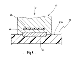
- the number 46 represents a hot stamp that with an electrical insulation 48 embedded heater 50 is equipped.
- Figure 8 serves thus to illustrate an embodiment of a Process for producing the radar sensor 10.
- Der Hot stamping stamp 46 is made by an electrical in a insulating mass 48 embedded electric heater 48 heated.
- the hot stamp 46 holds one Radiation area 28 in thermal contact, so that the Heat of the hot stamp 46 on the radiation surface 28 is transmitted.
- the metal rectangles of the patches Radiation areas were preferred beforehand using the Hot stamping stamp punched out of a metal foil.
- the hot stamp 46 in the Representation of Figure 8 down to the detail shown structure of the housing 12 pressed so that the heated radiation surface 28 hot into the housing structure 12 is embossed and an intimate connection with the material the housing structure 12 is received.
- the metal foil from which the patches were punched out can be coated with a pad that is used at elevated Temperature becomes sticky so it gets through the stamp too an adhesive comes with the plastic housing.
- the patches are heated up so much that they when stamping the plastic surface of the housing melt.
- the radiation surface 28 can both in a the inner surface 42 of the housing facing the ground surface 24 12 as well as in an outer surface facing away from the ground surface 24 Page 44 of the housing structure 12 are embossed.
- An alternative variant is in a wet chemical Process a metal layer is applied. The patches are lasered out of this metal layer or etched out.
Landscapes
- Physics & Mathematics (AREA)
- Electromagnetism (AREA)
- Engineering & Computer Science (AREA)
- Computer Security & Cryptography (AREA)
- Radar, Positioning & Navigation (AREA)
- Remote Sensing (AREA)
- Radar Systems Or Details Thereof (AREA)
- Variable-Direction Aerials And Aerial Arrays (AREA)
- Support Of Aerials (AREA)
- Details Of Aerials (AREA)
Abstract
Description
Die Erfindung betrifft darüber hinaus ein Verfahren zur Herstellung eines Radarsensors, der die genannten Merkmale aufweist.
Weiter ist bevorzugt, dass ein als Dielektrikum dienendes Luftvolumen durch eine zwischen der Strahlungsfläche und der Massefläche angeordnete Ausnehmung in der Verstärkungsstruktur definiert wird.
- Fig. 1
- schematisch eine Gesamtansicht eines Radarsensors für Kraftfahrzeuganwendungen;
- Fig. 2
- eine schematische Schnittdarstellung des Radarsensors nach Fig. 1 mit einem inneren Aufbau, wie er aus dem Stand der Technik bekannt ist;
- Fig. 3
- eine schematische Schnittdarstellung eines Radarsensors nach Fig. 1 mit einer ersten Ausgestaltung eines erfindungsgemäßen Aufbaus;
- Fig. 4
- eine schematische Schnittdarstellung einer zweiten Ausgestaltung eines erfindungsgemäßen Aufbaus;
- Fig. 5
- eine perspektivische Darstellung eines Teils eines Gehäuse eines Radarsensors;
- Fig. 6
- eine perspektivische Darstellung eines Teils einer Verstärkungsstruktur;
- Fig. 7
- eine perspektivische Darstellung eines Teils einer Massefläche auf einem Hochfrequenzsubstrat; und
- Fig. 8
- einen Heißprägeschritt im Rahmen eines erfindungsgemäßen Verfahrens.
Claims (10)
- Radarantenne (10) für Kraftfahrzeuganwendungen mit wenigstens einem Speisenetzwerk (18) auf einer ersten Seite (20) eines Hochfrequenzsubstrates (22), einer metallischen Massefläche (24) auf einer zweiten Seite (26) des Hochfrequenzsubstrates (22), die dem Speisenetzwerk (18) gegenüberliegt, und mit wenigstens einer Strahlungsfläche (28), die über eine zugeordnete Apertur (30) in der metallischen Massefläche (24) und über ein zwischen Massefläche (24) und Strahlungsfläche (28) angeordnetes Dielektrikum (32) von dem Speisenetzwerk (18) zur Abstrahlung elektromagnetischer Wellen angeregt wird, und mit einem Gehäuse (12), dadurch gekennzeichnet, dass die Strahlungsfläche (28) fest mit dem Gehäuse (12) verbunden ist.
- Radarantenne (10) nach Anspruch 1, gekennzeichnet durch Luft als Dielektrikum.
- Radarantenne (10) nach Anspruch 1 oder 2, dadurch gekennzeichnet, dass zwischen der Massefläche (24) und dem Gehäuse (12) oder der Ebene der Strahlungsfläche (28) eine Verstärkungsstruktur (34) angeordnet ist, deren Dicke (36) den Abstand (38) der Massefläche (24) von der Strahlungsfläche (28) definiert.
- Radarantenne (10) nach Anspruch 2 und 3, dadurch gekennzeichnet, dass ein als Dielektrikum (32) dienendes Luftvolumen (72) durch eine zwischen der Strahlungsfläche (28) und der Massefläche (24) angeordnete Ausnehmung (40) in der Verstärkungsstruktur (34) definiert wird.
- Radarantenne (10) nach einem der vorhergehenden Ansprüche, dadurch gekennzeichnet, dass die wenigstens eine Strahlungsfläche (28) auf einer der Massefläche (24) zugewandten Seite (42) des Gehäuses (12) angeordnet ist.
- Radarantenne (10) nach einem der Ansprüche 1 bis 4, dadurch gekennzeichnet, dass die wenigstens eine Strahlungsfläche (28) auf einer der Massefläche (24) gegenüberliegenden, abgewandten Seite (44) des Gehäuses (12) angeordnet ist.
- Verfahren zur Herstellung eines Radarsensors (10) für Kraftfahrzeuganwendungen mit wenigstens einem Speisenetzwerk (18) auf einer ersten Seite (20) eines Hochfrequenzsubstrates (22), einer metallischen Massefläche (24) auf einer zweiten Seite (24) des Hochfrequenzsubstrates (22), die dem Speisenetzwerk (18) gegenüberliegt, und mit wenigstens einer Strahlungsfläche (28), die über eine zugeordnete Apertur (30) in der metallischen Massefläche (24) und über ein zwischen Massefläche (24) und Strahlungsfläche (28) angeordnetes Dielektrikum (32) von dem Speisenetzwerk (18) zur Abstrahlung elektromagnetischer Wellen angeregt wird, und mit einem Gehäuse (12), dadurch gekennzeichnet, dass die Strahlungsfläche (28) fest mit dem Gehäuse (12) verbunden wird.
- Verfahren nach Anspruch 5, dadurch gekennzeichnet, dass die feste Verbindung der wenigstens einen Strahlungsfläche (28) mit dem Gehäuse (12) dadurch erzeugt wird, dass wenigstens eine vorgefertigte metallische Strahlungsfläche (28) durch einen Heißprägeprozess auf das Gehäuse (12) gepresst wird.
- Verfahren nach Anspruch 5, dadurch gekennzeichnet, dass die feste Verbindung der wenigstens einen Strahlungsfläche (28) mit dem Gehäuse (12) dadurch erzeugt wird, dass wenigstens eine vorgefertigte metallische Strahlungsfläche (28) mit dem Gehäuse (12) verklebt wird.
- Verfahren nach Anspruch 5, dadurch gekennzeichnet, dass die feste Verbindung der wenigstens einen Strahlungsfläche (28) mit dem Gehäuse (12) dadurch erzeugt wird, dass wenigstens ein Teil des Gehäuses (12) metallisch beschichtet wird und dass die Beschichtung anschließend mit der Ausnahme einer vorbestimmten Strahlungsfläche (28) durch einen Ätzprozess entfernt wird oder dass die Strahlungsflächen mit einem Laser ausgeschnitten werden.
Applications Claiming Priority (2)
| Application Number | Priority Date | Filing Date | Title |
|---|---|---|---|
| DE10318815 | 2003-04-17 | ||
| DE10318815A DE10318815A1 (de) | 2003-04-17 | 2003-04-17 | Schlitzgekoppelte Radarantenne mit Strahlungsflächen |
Publications (2)
| Publication Number | Publication Date |
|---|---|
| EP1469552A2 true EP1469552A2 (de) | 2004-10-20 |
| EP1469552A3 EP1469552A3 (de) | 2004-12-22 |
Family
ID=32892452
Family Applications (1)
| Application Number | Title | Priority Date | Filing Date |
|---|---|---|---|
| EP04003723A Withdrawn EP1469552A3 (de) | 2003-04-17 | 2004-02-19 | Schlitzgekoppelte Radarantenne mit Strahlungsflächen |
Country Status (3)
| Country | Link |
|---|---|
| US (1) | US20040239571A1 (de) |
| EP (1) | EP1469552A3 (de) |
| DE (1) | DE10318815A1 (de) |
Cited By (2)
| Publication number | Priority date | Publication date | Assignee | Title |
|---|---|---|---|---|
| WO2010066434A1 (de) * | 2008-12-13 | 2010-06-17 | Valeo Schalter Und Sensoren Gmbh | Steckerverbindungen an radarsensoren und verfahren zu deren herstellung |
| WO2012034762A1 (de) * | 2010-09-15 | 2012-03-22 | Robert Bosch Gmbh | Planare gruppenantenne mit in mehreren ebenen angeordneten antennenelementen |
Families Citing this family (10)
| Publication number | Priority date | Publication date | Assignee | Title |
|---|---|---|---|---|
| EP1624527B1 (de) * | 2003-04-24 | 2012-05-09 | Asahi Glass Company, Limited | Antenneneinrichtung |
| US8031129B2 (en) | 2004-08-18 | 2011-10-04 | Ruckus Wireless, Inc. | Dual band dual polarization antenna array |
| US7391382B1 (en) * | 2005-04-08 | 2008-06-24 | Raytheon Company | Transmit/receive module and method of forming same |
| US7511664B1 (en) | 2005-04-08 | 2009-03-31 | Raytheon Company | Subassembly for an active electronically scanned array |
| US7456789B1 (en) | 2005-04-08 | 2008-11-25 | Raytheon Company | Integrated subarray structure |
| JP4498292B2 (ja) * | 2006-03-07 | 2010-07-07 | 株式会社東芝 | 半導体モジュール及び半導体モジュールの製造方法 |
| US8698675B2 (en) | 2009-05-12 | 2014-04-15 | Ruckus Wireless, Inc. | Mountable antenna elements for dual band antenna |
| US9407012B2 (en) | 2010-09-21 | 2016-08-02 | Ruckus Wireless, Inc. | Antenna with dual polarization and mountable antenna elements |
| US9570799B2 (en) | 2012-09-07 | 2017-02-14 | Ruckus Wireless, Inc. | Multiband monopole antenna apparatus with ground plane aperture |
| EP2974045A4 (de) | 2013-03-15 | 2016-11-09 | Ruckus Wireless Inc | Niedrigbandreflektor für eine gerichtete doppelbandantenne |
Family Cites Families (18)
| Publication number | Priority date | Publication date | Assignee | Title |
|---|---|---|---|---|
| JPS63258102A (ja) * | 1987-04-15 | 1988-10-25 | Matsushita Electric Works Ltd | 平面アンテナ |
| US4973972A (en) * | 1989-09-07 | 1990-11-27 | The United States Of America As Represented By The Administrator Of The National Aeronautics And Space Adminstration | Stripline feed for a microstrip array of patch elements with teardrop shaped probes |
| CA2061254C (en) * | 1991-03-06 | 2001-07-03 | Jean Francois Zurcher | Planar antennas |
| EP0815613A1 (de) * | 1995-03-20 | 1998-01-07 | Minnesota Mining And Manufacturing Company | Doppelfrequenzantenne mit integrietem diplexer |
| JP2957463B2 (ja) * | 1996-03-11 | 1999-10-04 | 日本電気株式会社 | パッチアンテナおよびその製造方法 |
| US5859614A (en) * | 1996-05-15 | 1999-01-12 | The United States Of America As Represented By The Secretary Of The Army | Low-loss aperture-coupled planar antenna for microwave applications |
| JP2956598B2 (ja) * | 1996-07-31 | 1999-10-04 | 日本電気株式会社 | 平面アンテナ |
| GB2320815B (en) * | 1996-12-23 | 2001-12-12 | Nokia Mobile Phones Ltd | Antenna assembly |
| JPH10242733A (ja) * | 1997-02-25 | 1998-09-11 | Aisin Seiki Co Ltd | 車両用アンテナ内蔵外装部品 |
| CN2329091Y (zh) * | 1998-06-12 | 1999-07-14 | 庄昆杰 | 一种宽频带微带阵列天线单元 |
| US6118405A (en) * | 1998-08-11 | 2000-09-12 | Nortel Networks Limited | Antenna arrangement |
| FR2784506A1 (fr) * | 1998-10-12 | 2000-04-14 | Socapex Amphenol | Antenne a plaque |
| US6563042B2 (en) * | 1999-05-21 | 2003-05-13 | Intel Corporation | Radiating enclosure |
| WO2001020720A1 (en) * | 1999-09-14 | 2001-03-22 | Paratek Microwave, Inc. | Serially-fed phased array antennas with dielectric phase shifters |
| JP2001177332A (ja) * | 1999-12-17 | 2001-06-29 | Matsushita Electric Works Ltd | レーダー装置 |
| US6266015B1 (en) * | 2000-07-19 | 2001-07-24 | Harris Corporation | Phased array antenna having stacked patch antenna element with single millimeter wavelength feed and microstrip quadrature-to-circular polarization circuit |
| DE10063437A1 (de) * | 2000-12-20 | 2002-07-11 | Bosch Gmbh Robert | Antennenanordnung |
| US6624787B2 (en) * | 2001-10-01 | 2003-09-23 | Raytheon Company | Slot coupled, polarized, egg-crate radiator |
-
2003
- 2003-04-17 DE DE10318815A patent/DE10318815A1/de not_active Withdrawn
-
2004
- 2004-02-19 EP EP04003723A patent/EP1469552A3/de not_active Withdrawn
- 2004-04-01 US US10/814,130 patent/US20040239571A1/en not_active Abandoned
Cited By (5)
| Publication number | Priority date | Publication date | Assignee | Title |
|---|---|---|---|---|
| WO2010066434A1 (de) * | 2008-12-13 | 2010-06-17 | Valeo Schalter Und Sensoren Gmbh | Steckerverbindungen an radarsensoren und verfahren zu deren herstellung |
| US8545266B2 (en) | 2008-12-13 | 2013-10-01 | Valeo Schalter Und Sensoren Gmbh | Plug connections on radar sensors and method for their production |
| CN102246617B (zh) * | 2008-12-13 | 2014-07-02 | 法雷奥开关和传感器有限责任公司 | 雷达传感器上的插头连接件及其制造方法 |
| WO2012034762A1 (de) * | 2010-09-15 | 2012-03-22 | Robert Bosch Gmbh | Planare gruppenantenne mit in mehreren ebenen angeordneten antennenelementen |
| US9653807B2 (en) | 2010-09-15 | 2017-05-16 | Robert Bosch Gmbh | Planar array antenna having antenna elements arranged in a plurality of planes |
Also Published As
| Publication number | Publication date |
|---|---|
| DE10318815A1 (de) | 2004-11-04 |
| US20040239571A1 (en) | 2004-12-02 |
| EP1469552A3 (de) | 2004-12-22 |
Similar Documents
| Publication | Publication Date | Title |
|---|---|---|
| EP1782502B1 (de) | Antennenstruktur mit patch-elementen | |
| DE69512865T2 (de) | Scheibenantenne | |
| DE3727178C2 (de) | ||
| EP2532048B1 (de) | Gestapelte mikrostreifen-antenne | |
| DE10318815A1 (de) | Schlitzgekoppelte Radarantenne mit Strahlungsflächen | |
| WO2006032579A1 (de) | Trägeranordnung für eine hochfrequenzantenne und verfahren zu ihrer herstellung | |
| DE19963004A1 (de) | Kraftfahrzeug-Radarsystem | |
| WO2022053114A1 (de) | Radarsystem zur umgebungserfassung mit einer wellenleiterantenne gebildet aus einer platine und einem formteil | |
| CH704552A1 (de) | Gruppenantenne. | |
| EP3029770A1 (de) | Planarantenne mit abdeckung | |
| DE112008001263T5 (de) | Fahrzeugspiegel-Antennenbaugruppe | |
| WO1996031918A1 (de) | Antennenanordnung auf einem fenster mit hoher wärmetransmissionsdämpfung | |
| DE60213057T2 (de) | Befestigungsanordnung für Hochfrequenz-Halbleitervorrichtung und zugehöriges Herstellungsverfahren | |
| EP1820237A1 (de) | Vorrichtung zum aussenden und/oder empfangen von hochfrequenzsignalen in ein offenes oder ein geschlossenes raumsystem | |
| DE102011079646A1 (de) | Ultraschallsensorvorrichtung zum Erfassen und/oder Senden von Ultraschall | |
| DE102006027694B3 (de) | Mehrschichtige Antenne planarer Bauart | |
| EP1623248A1 (de) | Radarsensor f r automobilanwendungen | |
| EP3956944B1 (de) | Leiterplatten-antenne | |
| DE112020000022T5 (de) | Verfahren zur herstellung einer heckscheibe für fahrzeuge ausgestattet mit einer in die heizung integrierten antenne | |
| DE102013202806A1 (de) | Schaltung auf dünnem Träger für den Einsatz in Hohlleitern und Herstellungsverfahren | |
| DE102004041644A1 (de) | Transponder | |
| DE102004001899A1 (de) | Sperrkreisanordnung | |
| DE10322803A1 (de) | Mikrostreifenantenne | |
| DE102020102546A1 (de) | Verfahren und Messgerät zur Folienmetallisierung | |
| EP2983008A1 (de) | Sensorvorrichtung mit kombiniertem ultraschallsensor und radarsensor zum erfassen eines objekts in einem umfeld eines kraftfahrzeugs und kraftfahrzeug |
Legal Events
| Date | Code | Title | Description |
|---|---|---|---|
| PUAI | Public reference made under article 153(3) epc to a published international application that has entered the european phase |
Free format text: ORIGINAL CODE: 0009012 |
|
| AK | Designated contracting states |
Kind code of ref document: A2 Designated state(s): AT BE BG CH CY CZ DE DK EE ES FI FR GB GR HU IE IT LI LU MC NL PT RO SE SI SK TR |
|
| AX | Request for extension of the european patent |
Extension state: AL LT LV MK |
|
| PUAL | Search report despatched |
Free format text: ORIGINAL CODE: 0009013 |
|
| AK | Designated contracting states |
Kind code of ref document: A3 Designated state(s): AT BE BG CH CY CZ DE DK EE ES FI FR GB GR HU IE IT LI LU MC NL PT RO SE SI SK TR |
|
| AX | Request for extension of the european patent |
Extension state: AL LT LV MK |
|
| RIN1 | Information on inventor provided before grant (corrected) |
Inventor name: KUENZLER, FRANK Inventor name: WALZ, DIRK Inventor name: BIEHLMAN, BERND Inventor name: PAPZINER, UWE |
|
| 17P | Request for examination filed |
Effective date: 20050225 |
|
| 17Q | First examination report despatched |
Effective date: 20050415 |
|
| AKX | Designation fees paid |
Designated state(s): AT BE BG CH CY CZ DE DK EE ES FI FR GB GR HU IE IT LI LU MC NL PT RO SE SI SK TR |
|
| STAA | Information on the status of an ep patent application or granted ep patent |
Free format text: STATUS: THE APPLICATION IS DEEMED TO BE WITHDRAWN |
|
| 18D | Application deemed to be withdrawn |
Effective date: 20051026 |