EP1469501A2 - Plasmaanzeigetafel - Google Patents
Plasmaanzeigetafel Download PDFInfo
- Publication number
- EP1469501A2 EP1469501A2 EP04006944A EP04006944A EP1469501A2 EP 1469501 A2 EP1469501 A2 EP 1469501A2 EP 04006944 A EP04006944 A EP 04006944A EP 04006944 A EP04006944 A EP 04006944A EP 1469501 A2 EP1469501 A2 EP 1469501A2
- Authority
- EP
- European Patent Office
- Prior art keywords
- electrodes
- transparent ito
- metal electrodes
- display panel
- plasma display
- Prior art date
- Legal status (The legal status is an assumption and is not a legal conclusion. Google has not performed a legal analysis and makes no representation as to the accuracy of the status listed.)
- Withdrawn
Links
Images


Classifications
-
- H—ELECTRICITY
- H01—ELECTRIC ELEMENTS
- H01J—ELECTRIC DISCHARGE TUBES OR DISCHARGE LAMPS
- H01J11/00—Gas-filled discharge tubes with alternating current induction of the discharge, e.g. alternating current plasma display panels [AC-PDP]; Gas-filled discharge tubes without any main electrode inside the vessel; Gas-filled discharge tubes with at least one main electrode outside the vessel
- H01J11/20—Constructional details
- H01J11/22—Electrodes, e.g. special shape, material or configuration
- H01J11/24—Sustain electrodes or scan electrodes
-
- H—ELECTRICITY
- H01—ELECTRIC ELEMENTS
- H01J—ELECTRIC DISCHARGE TUBES OR DISCHARGE LAMPS
- H01J11/00—Gas-filled discharge tubes with alternating current induction of the discharge, e.g. alternating current plasma display panels [AC-PDP]; Gas-filled discharge tubes without any main electrode inside the vessel; Gas-filled discharge tubes with at least one main electrode outside the vessel
- H01J11/10—AC-PDPs with at least one main electrode being out of contact with the plasma
- H01J11/12—AC-PDPs with at least one main electrode being out of contact with the plasma with main electrodes provided on both sides of the discharge space
-
- H—ELECTRICITY
- H01—ELECTRIC ELEMENTS
- H01J—ELECTRIC DISCHARGE TUBES OR DISCHARGE LAMPS
- H01J2211/00—Plasma display panels with alternate current induction of the discharge, e.g. AC-PDPs
- H01J2211/20—Constructional details
- H01J2211/22—Electrodes
- H01J2211/24—Sustain electrodes or scan electrodes
- H01J2211/245—Shape, e.g. cross section or pattern
-
- H—ELECTRICITY
- H01—ELECTRIC ELEMENTS
- H01J—ELECTRIC DISCHARGE TUBES OR DISCHARGE LAMPS
- H01J2211/00—Plasma display panels with alternate current induction of the discharge, e.g. AC-PDPs
- H01J2211/20—Constructional details
- H01J2211/22—Electrodes
- H01J2211/32—Disposition of the electrodes
- H01J2211/323—Mutual disposition of electrodes
Definitions
- the present invention relates to a plasma display panel and more specifically to a plasma display panel in which metal and auxiliary metal electrodes are formed such that brightness and efficiency are improved.
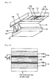
- FIG. 1 is a perspective view illustrating a discharge cell of a general AC plasma display panel arranged in matrix shape.
- a conventional PDP comprises a front substrate 10 and rear substrate 12.
- a pair of sustain electrode 14, 16, upper dielectric layer 18 and protective layer 20 are gradually formed on the front substrate 10
- address electrodes 22, lower dielectric layer 24 and barrier ribs 26 and phosphor layer 28 are gradually formed on the rear substrate 12.
- the front substrate 10 and the rear substrate 12 are spaced in parallel to each other at a predetermined distance by barrier ribs 26.
- the protection layer 20 serves to prevent damage of the upper dielectric layer 18 due to sputtering generated upon the plasma discharge and to increase emission efficiency of secondary electrons.
- the protection layer 20 is usually formed using magnesium oxide (MgO).
- the address electrodes 22 are formed in the direction intersecting a pair of sustain electrodes 14, 16. A data signal is supplied for the address electrodes 22 to select a cell that is displayed.
- the barrier ribs 26 are formed in parallel to the address electrode 22 and serves to prevent ultraviolet rays and a visible ray generated due to the discharge from leaking toward neighboring discharge cells.
- the barrier ribs 26 may be existed or not a boundary line of sub-pixel.
- the phosphor layer 28 is excited by ultraviolet rays generated upon the plasma discharge to generate a visible ray of one of red, green and blue.
- Inert mixed gases such as He + Xe, Ne + Xe and He + Ne + Xe for discharge are inserted into a discharge space of the discharge cell formed between the upper/lower substrates 10, 12.
- a pair of sustain electrode 14, 16 comprises scan electrodes 14 and sustain electrodes 16.
- a scan signal for scanning of the panel is supplied for scan electrodes 14 and a sustain signal for maintaining discharge of a selected cell is supplied for sustain electrodes.
- a pair of sustain electrode 14, 16 comprises transparent ITO electrodes 14A, 16A, which are stripe pattern, are made of transparent material in order to transmit a visible ray and have a wide width relatively, and metal electrodes 14B, 16B, which compensate a resistance of transparent ITO electrodes 14A, 16A and have a narrow width relatively.
- Each of the transparent ITO electrodes of a pair of sustain electrodes 14, 16 is opposite to each other at a predetermined distance.
- metal electrodes 14B, 16B are formed in parallel to the transparent ITO electrodes 14A, 16A and formed on a verge of the transparent ITO electrodes 14A, 16A, respectively. Namely, metal electrodes 14B, 16B are formed on outside verge of the transparent ITO electrodes 14A, 16A.
- a PDP cell of this structure sustains a discharge according to surface discharge between a pair of sustain electrodes 14, 16 after being selected by opposite discharge between the address electrode 22 and the scan electrode 14.
- a visible ray is emitted to an outside of cell as radiating phosphors 28 by ultraviolet rays which are generated while the sustain discharge occurs.
- the PDP having cells displays an image.
- the PDP realizes a gray scale by controlling the discharge sustaining period, i.e. the number of sustain discharge according to a video data.
- Xe inert gas excites phosphors 28 using a vacuum ultraviolet generated by changing from excited state to ground state according to gas discharge. Therefore, as a content of Xe is much, a quantity of vacuum ultraviolet rays generated upon the gas discharge and the efficiency of the PDP increase. However, the increase of Xe is caused by rising discharge starting voltage and discharge sustaining voltage between sustain electrodes.
- the discharge starting voltage and the discharge sustaining voltage is rose because the metal electrodes 14B, 16B are formed on the outside verge of the transparent ITO electrodes 14A, 16A, respectively. Also, the brightness and efficiency of the conventional PDP are decreased.
- the conventional PDP structure has a difficulty in increasing brightness and efficiency without any problem such as the structure of electrodes within the discharge cell.
- the present invention has been made in view of the above problems, and it is an object of the present invention to provide a plasma display panel for increasing brightness and efficiency and improving a stability of discharge.
- a plasma display panel comprises: transparent ITO electrodes which are spaced in parallel to each other at a predetermined distance within a discharge cell; metal electrodes which are formed on said transparent ITO electrodes and in parallel to said transparent ITO electrodes so that are positioned in the direction of opposite sides of said transparent ITO electrodes, respectively.
- a plasma display panel comprises: transparent ITO electrodes which are spaced in parallel to each other at a predetermined distance within a discharge cell and are patterned so that a part of said transparent ITO electrodes is different in width, respectively; and metal electrodes which are formed on said transparent ITO electrodes and in parallel to said transparent ITO electrodes so that are positioned in the direction of opposite sides of said transparent ITO electrodes, respectively.
- a plasma display panel comprises: transparent ITO electrodes which are spaced in parallel to each other at a predetermined distance within a discharge cell; metal electrodes which are formed on said transparent ITO electrodes and in parallel to said transparent ITO electrodes so that are positioned in the direction of opposite sides of said transparent ITO electrodes, respectively; and projecting metal electrodes which are jutted from said metal electrodes, respectively.
- FIG. 1 is a perspective view illustrating a discharge cell of a plasma display panel of the prior art.
- FIG. 2 is a plane view illustrating a pair of sustain electrodes shown in FIG. 1.
- FIG. 3 is a perspective view illustrating a discharge cell of a plasma display panel according to a first embodiment of the present invention.
- FIG. 4 is a plane view illustrating a pair of sustain electrodes according to the first embodiment of the present invention shown in FIG. 3.
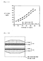
- FIG. 5 is a graph showing comparison of brightness between the first embodiment of the present invention and the prior art with respect to discharge voltage.
- FIG. 6 is a graph showing comparison of efficiency between the first embodiment of the present invention and the prior art with respect to discharge voltage.
- FIG. 7 is a plane view illustrating a pair of sustain electrodes according to a modification of the first embodiment.
- FIG. 8a is a plane view illustrating a pair of sustain electrodes according to another modification of a first embodiment.
- FIG. 8b is a cross-sectional view of a pair of sustain electrodes of FIG. 8a taken along a line A-A'.
- FIG. 9 is a perspective view illustrating a discharge cell of a plasma display panel according to a second embodiment of the present invention.
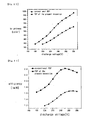
- FIG. 10 is a graph showing comparison of brightness between the second embodiment of the present invention and the prior art with respect to discharge voltage.
- FIG. 11 is a graph showing comparison of efficiency between the second embodiment of the present invention and the prior art with respect to discharge voltage.
- FIG. 12 is a plane view illustrating a pair of sustain electrodes according to a modification of the second embodiment.
- FIG. 13 is a graph showing comparison of brightness between a modification of the second embodiment of the present invention and the prior art with respect to discharge voltage.
- FIG. 14 is a graph showing comparison of efficiency between a modification of the second embodiment of the present invention and the prior art with respect to discharge voltage.
- FIG. 15 is a plane view illustrating a pair of sustain electrodes according to another modification of the second embodiment.
- FIG. 16 is a plane view illustrating a pair of sustain electrodes according to a third embodiment of the present invention.
- FIG. 17 is a graph showing comparison of brightness between the third embodiment of the present invention and the prior art with respect to discharge voltage.
- FIG. 18 is a graph showing comparison of efficiency between the third embodiment of the present invention and the prior art with respect to discharge voltage.
- FIG. 19 is a plane view illustrating a pair of sustain electrodes according to a modification of the third embodiment.
- FIG. 20 is a plane view illustrating a pair of sustain electrodes according to another modification of the third embodiment.
- FIG. 21 is a plane view illustrating a pair of sustain electrodes according to the other modification of the third embodiment.
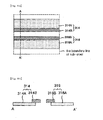
- FIG. 3 is a perspective view illustrating a discharge cell of a plasma display panel according to a first embodiment of the present invention
- FIG. 4 is a plane view illustrating a pair of sustain electrodes according to the first embodiment of the present invention shown in FIG. 3.
- a plasma display panel has a front substrate 110 and rear substrate 112.
- a pair of sustain electrodes 114, 116, upper dielectric layer 118 and protective layer 120 are gradually formed on the front substrate 110
- address electrodes 122, lower dielectric layer 124 and barrier ribs 126 and phosphor layer 28 are gradually formed on the rear substrate 112.
- the front substrate 110 and the rear substrate 112 are spaced in parallel to each other at a predetermined distance by barrier ribs 126.
- a pair of sustain electrode 114, 116 is composed of scan electrodes 114 and sustain electrodes 116.
- a scan signal for scanning of the panel is supplied for scan electrodes 114 and a sustain signal for maintaining discharge of a selected cell is supplied for sustain electrodes 116.
- the sustain electrodes 114, 116 are consisted of the transparent ITO electrodes 114A, 116A and the metal electrodes 114B, 116B.
- the transparent ITO electrodes 1 14A, 116A have a stripe pattern of a wide width relatively and are made of transparent material in order to transmit a visible ray.
- the metal electrodes 114B, 116B have a stripe pattern of a narrow width relatively and are made of material having a good conductivity in order to compensate a conductivity of transparent ITO electrodes 114A,116A.
- Each of the transparent ITO electrodes 1 14A, 116A of a pair of sustain electrodes 114, 116 are opposite to each other at a predetermined distance.
- each of the metal electrodes 114B, 116B satisfies the following the equation 1.
- Equation.1 d2 ⁇ d1/2 wherein d1 represents a distance between a central portion of the transparent ITO electrodes 114A, 116A and a center line(Pc) of the discharge cell, d2 represents a distance between a central portion of the metal electrodes 114B, 116B and a center line(Pc) of the discharge cell .
- the discharge starting voltage and discharge sustaining voltage are decreased and the brightness and efficiency are increased at this time of the discharge, although the contents of Xe inert gas increases.
- the strong electric field generates at the central portion of the discharge cell, at this time of the discharge. And, the discharge starting voltage and discharge sustaining voltage are decreased by the strong electric field generates at the central portion of the discharge cell.
- FIG. 5 is a brightness graph which is compared a first embodiment of the present invention with a prior art
- FIG. 6 is a efficiency graph which is compared a first embodiment of the present invention with a prior art.
- the brightness of the PDP according to the first embodiment of the present invention is improved the approximately 40% to 60% than the conventional PDP at the same discharge voltage
- the efficiency of the PDP according to the first embodiment of the present invention is improved the approximately 40% to 60% than the conventional PDP at the same discharge voltage. Further, as the discharge starting voltage and the discharge delay time are decreased, the stability of discharge can be improved.
- FIG. 7 is a plane view illustrating a pair of sustain electrodes according to a modification of the first embodiment.
- sustain electrodes 214, 216 are consisted of transparent ITO electrodes 214A, 216A and metal electrodes 214B, 216B on the transparent ITO electrodes 214A, 216A.
- the transparent ITO electrodes 214A, 216A have a stripe pattern of a wide width relatively and are made of transparent material in order to transmit a visible ray.
- Each of the metal electrodes 214B, 216B has a stripe pattern which is a narrow wide than the transparent ITO electrodes 214A, 216A and is formed in the direction of a central portion of the transparent ITO electrodes 214A, 216A from a opposite sides of the transparent ITO electrodes 214A, 216A. Further, a position of the metal electrodes 214B, 216B satisfies the above equation 1 and the metal electrodes 214B, 216B are made of material having a good conductivity in order to compensate a conductivity of transparent ITO electrodes 214A, 216A.
- a distance between the metal electrodes 214B, 216B according to a modification of the first embodiment is near than a distance between the metal electrodes 114B, 116B according to the first embodiment. Therefore, a strong electric field is induced at the central portion (Pc) of the discharge cell when the plasma discharge occurs.
- a characteristic of the brightness and efficiency is similar to those of the first embodiment shown in FIG. 5 and FIG. 6.
- FIG. 8a is a plane view illustrating a pair of sustain electrodes according to another modification of a first embodiment
- FIG. 8b is a cross-sectional view of a pair of sustain electrodes of FIG. 8a taken along a line A-A'.
- Transparent ITO electrodes 314A, 31 6A have a stripe pattern of a wide width relatively and are made of transparent material in order to transmit a visible ray.
- Each of the metal electrodes 314B, 316B has a stripe pattern which is a narrow wide than the transparent ITO electrodes 314A, 316A. A part of each of the metal electrodes 314B, 316B is formed on an opposite sides of the transparent ITO electrodes 314A, 316A. Further, a position of the metal electrodes 314B, 316B satisfies the above equation 1 and the metal electrodes 314B, 316B are made of material having a good conductivity in order to compensate a conductivity of transparent ITO electrodes 314A, 316A.
- a distance between the metal electrodes 314B, 316B according to another modification of the first embodiment is near than a distance between the metal electrodes according to the first embodiment. Therefore, a strong electric field is induced at the central portion (Pc) of the discharge cell when the plasma discharge occurs.
- FIG. 9 is a perspective view illustrating a discharge cell of a plasma display panel according to a second embodiment of the present invention.
- Sustain electrodes 414, 416 are consisted of transparent ITO electrodes 414A, 416A and metal electrodes 414B, 416B on the transparent ITO electrodes 414A, 416A.
- the transparent ITO electrodes 414A, 416A are opposite to each other at a predetermined distance.
- the transparent ITO electrodes 414A, 41 6A have a stripe pattern of a wide width relatively and are made of transparent material in order to transmit a visible ray. And, each of the transparent ITO electrodes 414A, 416A is a "T" shape, namely both edges are patterned in a shape of quadrangle. Wherein the pattern is a part which an influence of brightness is little.
- each of the transparent ITO electrodes 414A, 416A satisfies the following the equation 2 and 3.
- Equation.1 0.2 ⁇ W1 ⁇ W2 ⁇ 0.8 ⁇ 1 wherein W1 represents a horizontal length of a discharge cell, W2 represents a horizontal length of a part of a narrow area of the transparent ITO electrodes 414A, 416A, relatively.
- Equation. 3 0.2 ⁇ D3 ⁇ D4 ⁇ 0.8 ⁇ D3 wherein D3 represents a width of the transparent ITO electrodes 414A, 41 6A, D4 represents a width of a part of a narrow area of the transparent ITO electrodes 414A, 41 6A, relatively.
- Each of the metal electrodes 414B, 416B has a stripe pattern which is narrow than a wide of the transparent ITO electrodes 414A, 41 6A and is formed in the direction of a central portion of the transparent ITO electrodes 414A, 41 6A from an opposite sides of the transparent ITO electrodes 414A, 416A. Further, a position of the metal electrodes 414B, 416B satisfies the above equation 1 and the metal electrodes 414B, 416B are made of material having a good conductivity in order to compensate a conductivity of transparent ITO electrodes 414A, 416A.
- the discharge starting voltage and discharge sustaining voltage are decreased and the brightness and efficiency are increased at this time of the discharge, although the contents of Xe inert gas increases. Further, as an area ratio of the transparent ITO electrodes 414A, 416A in comparison with a discharge cell is decreased, a consumption power is reduced and a radiation efficiency is improved.
- a current density according to the second embodiment of the present invention is decreased approximately 20% to 25% in comparison with the conventional PDP and a reductive width of the current density is larger as a discharge voltage is high.
- the efficiency of the PDP according to the second embodiment of the present invention is improved than the conventional PDP at the same discharge voltage.
- FIG. 12 is a plane view illustrating a pair of sustain electrodes according to a modification of the second embodiment.
- Sustain electrodes 514, 516 are consisted of transparent ITO electrodes 514A, 516A and metal electrodes 514B, 516B on the transparent ITO electrodes 514A, 516A.
- the transparent ITO electrodes 514A, 516A are opposite to each other at a predetermined distance.
- the transparent ITO electrodes 514A, 516A have a stripe pattern of a wide width relatively and are made of transparent material in order to transmit a visible ray. And, each of the transparent ITO electrodes 514A, 516A is consisted of an upper portion of a first width and a lower portion of a second width. Namely, both edges are patterned in a shape of triangle. Wherein the pattern is a part which an influence of brightness is little. In result, each of the transparent ITO electrodes 514A, 516A becomes a joined shape of quadrangle and trapezoid.
- Each of the metal electrodes 514B, 516B has a stripe pattern which is a narrow wide than the transparent ITO electrodes 514A, 516A and is formed in the direction of a central portion of the transparent ITO electrodes 514A, 516A from a opposite sides of the transparent ITO electrodes 514A, 516A. Further, the metal electrodes 514B, 516B are made of material having a good conductivity in order to compensate a conductivity of transparent ITO electrodes 514A, 516A.
- the discharge starting voltage and discharge sustaining voltage are decreased and the brightness and efficiency are increased at this time of the discharge, although the contents of Xe inert gas increases. Further, as an area ratio of the transparent ITO electrodes 514A, 516A in comparison with a discharge cell is decreased, a consumption power is reduced and a radiation efficiency is improved.
- a brightness of PDP according to a modification of the second embodiment is improved approximately 77% in comparison with the conventional PDP at a same discharge voltage.
- a efficiency of PDP according to the transformation of second embodiment is improved approximately 57% in comparison with the conventional PDP at a same discharge voltage.
- FIG. 15 is a plane view illustrating a pair of sustain electrodes according to another modification of the second embodiment.
- Sustain electrodes 614, 616 are consisted of transparent ITO electrodes 614A, 61 6A and metal electrodes 614B, 616B on the transparent ITO electrodes 614A, 616A.
- the transparent ITO electrodes 614A, 616A are opposite to each other at a predetermined distance.
- the transparent ITO electrodes 614A, 616A have a stripe pattern of a wide width relatively and are made of transparent material in order to transmit a visible ray. And, each of the transparent ITO electrodes 614A, 616A is consisted of an upper portion of a first width and a lower portion of a second width. Namely, both edges are patterned in a shape of trapezoid. Wherein the pattern is a part which an influence of brightness is little. In result, each of the transparent ITO electrodes 614A, 616A becomes a joined shape of stripe and trapezoid.
- Each of the metal electrodes 614B, 616B has a stripe pattern which is a narrow wide than the transparent ITO electrodes 614A, 616A and is formed in the direction of a central portion of the transparent ITO electrodes 614A, 616A from a opposite sides of the transparent ITO electrodes 614A, 616A. Further, the metal electrodes 614B, 616B are made of material having a good conductivity in order to compensate a conductivity of transparent ITO electrodes 614A, 616A.
- the discharge starting voltage and discharge sustaining voltage are decreased and the brightness and efficiency are increased at this time of the discharge, although the contents of Xe inert gas increases. Further, as an area ratio of the transparent ITO electrodes 614A, 616A in comparison with a discharge cell is decreased, a consumption power is reduced and a radiation efficiency is improved.
- FIG. 16 is a plane view illustrating a pair of sustain electrodes according to a third embodiment of the present invention.
- Sustain electrodes 714, 716 are consisted of transparent ITO electrodes 714A, 716A, metal electrodes 714B, 716B and projecting metal electrodes 714C, 716C on the transparent ITO electrodes 714A, 716A.
- the transparent ITO electrodes 714A, 716A are opposite to each other at a predetermined distance.
- the transparent ITO electrodes 714A, 716A have a stripe pattern of a wide width relatively and are made of transparent material in order to transmit a visible ray.
- Each of the metal electrodes 714B, 716B has a stripe pattern which is a narrow wide than the transparent ITO electrodes 714A, 716A and is formed in the direction of a central portion of the transparent ITO electrodes 714A, 716A from a opposite sides of the transparent ITO electrodes 714A, 716A. Further, the metal electrodes 714B, 716B are made of material having a good conductivity in order to compensate a conductivity of transparent ITO electrodes 714A, 716A.
- Each of the projecting metal electrodes 714C, 716C is jutted in the direction of a verge of a discharge cell from a middle point of the metal electrodes 714B, 716B. Whereupon, the projecting metal electrodes 714C, 716C and the metal electrodes 714B, 716B become a "T" shape.
- the projecting metal electrodes 714C, 716C are made of material having a good conductivity in order to compensate a conductivity of transparent ITO electrodes 714A, 716A, and are expanded in the direction of the outside sides of the discharge cell.
- each of the metal electrodes 714B, 716B satisfies the following the equation 4.
- Equation.4 D ⁇ H/4 wherein H represents a length of discharge cell, D represents a distance between a central portion of the metal electrodes 714B, 716B and a central portion of the discharge cell.
- the discharge starting voltage and discharge sustaining voltage are decreased and the brightness and efficiency are increased at this time of the discharge, although the contents of Xe inert gas increases. Further, as an area ratio of the transparent ITO electrodes 714A, 716A in comparison with a discharge cell is decreased, a consumption power is reduced and a radiation efficiency is improved.
- the strong electric field generates at the central portion of the discharge cell, at this time of the discharge, and then the discharge is expanded in the direction of the verge of the discharge cell.
- the discharge starting voltage and discharge sustaining voltage are decreased by the generated strong electric field at the central portion of the discharge cell and the brightness and efficiency are increased.
- the discharge starting voltage and the discharge delay time are decreased, the stability of the discharge is improved.
- a brightness of PDP according to the transformation of third embodiment is improved approximately 40% to 50% in comparison with the conventional PDP at a same discharge voltage.
- an efficiency of PDP according to the transformation of second embodiment is improved approximately 30% to 40% in comparison with the conventional PDP at a same discharge voltage.
- FIG. 19 is a plane view illustrating a pair of sustain electrodes according to a modification of the third embodiment.
- Sustain electrodes 814, 816 are consisted of transparent ITO electrodes 814A, 816A, metal electrodes 814B, 816B, projecting metal electrodes 814C, 816C and auxiliary metal electrodes 814D, 816D on the transparent ITO electrodes 814A, 816A.
- the transparent ITO electrodes 814A, 816A are opposite to each other at a predetermined distance.
- the transparent ITO electrodes 814A, 816A have a stripe pattern of a wide width relatively and are made of transparent material in order to transmit a visible ray.
- Each of the metal electrodes 814B, 816B has a stripe pattern which is a narrow wide than the transparent ITO electrodes 814A, 816A and is formed in the direction of a central portion of the transparent ITO electrodes 814A, 816A from a opposite sides of the transparent ITO electrodes 814A, 816A. Further, a position of the metal electrodes 814B, 816B satisfies the above equation 4 and the metal electrodes 8148, 816B are made of material having a good conductivity in order to compensate a conductivity of transparent ITO electrodes 814A, 816A.
- Each of the projecting metal electrodes 814C, 816C is jutted in the direction of a verge of a discharge cell from a middle point of the metal electrodes 814B, 816B. Whereupon, the projecting metal electrodes 814C, 816C and the metal electrodes 814B, 816B become a "T" shape.
- the projecting metal electrodes 814C, 816C are made of material having a good conductivity in order to compensate a conductivity of transparent ITO electrodes 814A, 816A, and are expanded in the direction of the outside sides of the discharge cell.
- Each of the auxiliary metal electrodes 814D, 816D is formed at a tip of the projecting metal electrodes 814C, 816C and formed in parallel to the metal electrodes 814B, 816B and is short than a length of the metal electrodes 814B, 816B.
- the metal electrodes 814B, 816B, the projecting metal electrodes 814C, 816C and the auxiliary metal electrodes 814D, 816D become a "H" shape.
- the auxiliary metal electrodes 814D, 816D are made of material having a good conductivity in order to compensate a conductivity of transparent ITO electrodes 814A, 816A, and are expanded in the direction of the outside sides of the discharge cell.
- the discharge starting voltage and discharge sustaining voltage are decreased and the brightness and efficiency are increased at this time of the discharge, although the contents of Xe inert gas increases. Further, as an area ratio of the transparent ITO electrodes 814A, 816A in comparison with a discharge cell is decreased, a consumption power is reduced and a radiation efficiency is improved.
- FIG. 20 is a plane view illustrating a pair of sustain electrodes according to another modification of the third embodiment.
- Sustain electrodes 914, 916 are consisted of transparent ITO electrodes 914A, 916A, metal electrodes 914B, 916B, projecting metal electrodes 914C, 916C and auxiliary metal electrodes 914D, 916D on the transparent ITO electrodes 914A, 916A.
- the transparent ITO electrodes 914A, 916A are opposite to each other at a predetermined distance.
- the transparent ITO electrodes 914A, 91 6A have a stripe pattern of a wide width relatively and are made of transparent material in order to transmit a visible ray.
- Each of the metal electrodes 914B, 916B has a stripe pattern which is a narrow wide than the transparent ITO electrodes 914A, 916A and is formed in the direction of a central portion of the transparent ITO electrodes 914A, 916A from a opposite sides of the transparent ITO electrodes 914A, 916A. Further, a position of the metal electrodes 914B, 916B satisfies the above equation 4 and the metal electrodes 914B, 916B are made of material having a good conductivity in order to compensate a conductivity of transparent ITO electrodes 914A, 916A.
- Each of the projecting metal electrodes 914C, 916C is jutted in the direction of a verge of a discharge cell from a middle point of the metal electrodes 914B, 916B. Whereupon, the projecting metal electrodes 914C, 916C and the metal electrodes 914B, 916B become a "T" shape.
- the projecting metal electrodes 914C, 916C are made of material having a good conductivity in order to compensate a conductivity of transparent ITO electrodes 914A, 916A, and are expanded in the direction of the outside sides of the discharge cell.
- Each of the auxiliary metal electrodes 914D, 916D is formed at a middle portion of the projecting metal electrodes 914C, 916C and formed in parallel to the metal electrodes 914B, 916B and is short than a length of the metal electrodes 914B, 916B.
- the metal electrodes 914B, 916B, the projecting metal electrodes 914C, 916C and the auxiliary metal electrodes 914D, 916D become a " ⁇ " shape.
- the auxiliary metal electrodes 914D, 916D are made of material having a good conductivity in order to compensate a conductivity of transparent ITO electrodes 914A, 916A, and are expanded in the direction of the outside sides of the discharge cell.
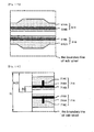
- FIG. 21 is a plane view illustrating a pair of sustain electrodes according to the other modification of the third embodiment.
- Sustain electrodes 1014, 1016 are consisted of transparent ITO electrodes 1014A, 1016A, metal electrodes 1014B, 1016B, projecting metal electrodes 1014C, 1016C and auxiliary metal electrodes 1014D, 1016D on the transparent ITO electrodes 1014A, 1016A.
- the transparent ITO electrodes 1014A, 1016A are opposite to each other at a predetermined distance.
- the transparent ITO electrodes 1014A, 1016A have a stripe pattern of a wide width relatively and are made of transparent material in order to transmit a visible ray.
- Each of the metal electrodes 1014B, 1016B has a stripe pattern which is narrow than a wide of the transparent ITO electrodes 1014A, 1016A and is formed in the direction of a central portion of the transparent ITO electrodes 1014A, 1016A from an opposite sides of the transparent ITO electrodes 1014A, 1016A. Further, a position of the metal electrodes 1014B, 1016B satisfies the above equation 4 and the metal electrodes 1014B, 1016B are made of material having a good conductivity in order to compensate a conductivity of transparent ITO electrodes 1014A, 1016A.
- Each of the projecting metal electrodes 1014C, 1016C is jutted in the direction of a verge of a discharge cell from a middle point of the metal electrodes 1014B, 1016B. Whereupon, the projecting metal electrodes 1014C, 1016C and the metal electrodes 1014B, 1016B become a "T" shape.
- the projecting metal electrodes 1014C, 1016C are made of material having a good conductivity in order to compensate a conductivity of transparent ITO electrodes 1014A, 1016A, and are expanded in the direction of the outside sides of the discharge cell.
- Each of the auxiliary metal electrodes 1014D, 1016D has a first auxiliary metal electrode and a second auxiliary metal electrode.
- the first auxiliary metal electrodes is formed at a tip of the projecting metal electrodes 1014C, 1016C and formed in parallel to the metal electrodes 1014B, 1016B and is short than a length of the metal electrodes 1014B, 1016B.
- the second auxiliary metal electrodes is formed at a middle portion of the projecting metal electrodes 1014C, 1016C and formed in parallel to the metal electrodes 1014B, 1016B and is short than a length of the metal electrodes 1014B, 1016B.
- the metal electrodes 1014B, 1016B, the projecting metal electrodes 1014C, 1016C and the auxiliary metal electrodes 1014D, 1016D become a " " shape.
- the auxiliary metal electrodes 1014D, 1016D are made of material having a good conductivity in order to compensate a conductivity of transparent ITO electrodes 1014A, 1016A, and are expanded in the direction of the outside sides of the discharge cell.
- a auxiliary metal electrode induces a strong electric field in the central portion of discharge cell and the discharge starting voltage and the discharge sustaining voltage are decreased. Therefore, the present invention has an effect that it can increase the brightness and efficiency at the same discharge voltage.
- the discharge starting voltage and discharge sustaining voltage are decreased and the brightness and efficiency are increased at this time of the discharge, although the contents of Xe inert gas increases. Further, as an area ratio of the transparent ITO electrodes in comparison with a discharge cell is decreased, a consumption power is reduced and a radiation efficiency is improved.
- a distance between metal electrodes is near, the strong electric field generates at the central portion of the discharge cell and the discharge is expanded in the direction of the verge of the discharge cell by a auxiliary metal electrode. Therefore, the discharge starting voltage and discharge sustaining voltage are decreased and the brightness and efficiency are increased at the same discharge voltage. Furthermore, as the discharge starting voltage and the discharge delay time are decreased, the stability of the discharge is improved.
Landscapes
- Engineering & Computer Science (AREA)
- Physics & Mathematics (AREA)
- Plasma & Fusion (AREA)
- Chemical & Material Sciences (AREA)
- Materials Engineering (AREA)
- Gas-Filled Discharge Tubes (AREA)
Applications Claiming Priority (6)
| Application Number | Priority Date | Filing Date | Title |
|---|---|---|---|
| KR2003018452 | 2003-03-25 | ||
| KR1020030018451A KR20040083801A (ko) | 2003-03-25 | 2003-03-25 | 플라즈마 디스플레이 패널 |
| KR1020030018452A KR20040083802A (ko) | 2003-03-25 | 2003-03-25 | 플라즈마 디스플레이 패널 |
| KR2003018451 | 2003-03-25 | ||
| KR2003035338 | 2003-06-02 | ||
| KR10-2003-0035338A KR100524305B1 (ko) | 2003-06-02 | 2003-06-02 | 플라즈마 디스플레이 패널 |
Publications (2)
| Publication Number | Publication Date |
|---|---|
| EP1469501A2 true EP1469501A2 (de) | 2004-10-20 |
| EP1469501A3 EP1469501A3 (de) | 2006-04-19 |
Family
ID=32912855
Family Applications (1)
| Application Number | Title | Priority Date | Filing Date |
|---|---|---|---|
| EP04006944A Withdrawn EP1469501A3 (de) | 2003-03-25 | 2004-03-23 | Plasmaanzeigetafel |
Country Status (4)
| Country | Link |
|---|---|
| US (3) | US7187126B2 (de) |
| EP (1) | EP1469501A3 (de) |
| JP (1) | JP2004296441A (de) |
| CN (1) | CN1532874A (de) |
Cited By (2)
| Publication number | Priority date | Publication date | Assignee | Title |
|---|---|---|---|---|
| EP1530228A3 (de) * | 2003-11-05 | 2006-07-05 | LG Electronics, Inc. | Plasma-Anzeigetafel |
| EP1465228A3 (de) * | 2003-03-25 | 2006-09-13 | LG Electronics Inc. | Plasmaanzeigetafel |
Families Citing this family (3)
| Publication number | Priority date | Publication date | Assignee | Title |
|---|---|---|---|---|
| KR100578924B1 (ko) * | 2004-05-28 | 2006-05-11 | 삼성에스디아이 주식회사 | 플라즈마 디스플레이 패널 |
| KR100647618B1 (ko) * | 2004-10-06 | 2006-11-23 | 삼성에스디아이 주식회사 | 플라즈마 디스플레이 패널 |
| KR100673437B1 (ko) * | 2004-12-31 | 2007-01-24 | 엘지전자 주식회사 | 플라즈마 디스플레이 패널 |
Family Cites Families (13)
| Publication number | Priority date | Publication date | Assignee | Title |
|---|---|---|---|---|
| JPH10333636A (ja) * | 1997-03-31 | 1998-12-18 | Mitsubishi Electric Corp | プラズマディスプレイパネル |
| JPH11212515A (ja) * | 1998-01-21 | 1999-08-06 | Hitachi Ltd | プラズマディスプレイ装置 |
| US6380677B1 (en) * | 1998-07-16 | 2002-04-30 | Lg Electronics Inc. | Plasma display panel electrode |
| JP3470629B2 (ja) * | 1999-02-24 | 2003-11-25 | 富士通株式会社 | 面放電型プラズマディスプレイパネル |
| JP2001160361A (ja) * | 1999-09-21 | 2001-06-12 | Mitsubishi Electric Corp | プラズマディスプレイパネル用基板及びプラズマディスプレイパネル |
| JP4069583B2 (ja) * | 2000-03-28 | 2008-04-02 | 三菱電機株式会社 | プラズマディスプレイ装置 |
| US6720736B2 (en) * | 2000-12-22 | 2004-04-13 | Lg Electronics Inc. | Plasma display panel |
| TW480517B (en) * | 2000-12-29 | 2002-03-21 | Acer Display Tech Inc | Electrode structure of plasma display panel |
| JP2002270100A (ja) * | 2001-03-12 | 2002-09-20 | Sony Corp | プラズマ放電表示装置 |
| JP2002298742A (ja) * | 2001-04-03 | 2002-10-11 | Nec Corp | プラズマディスプレイパネル、その製造方法及びプラズマ表示装置 |
| JP2002343235A (ja) * | 2001-05-14 | 2002-11-29 | Idemitsu Kosan Co Ltd | プラズマディスプレイパネル、プラズマディスプレイパネル用背面基板及び前面基板、及びプラズマディスプレイパネル配線用被覆金属粒子 |
| JP2003007216A (ja) * | 2001-06-25 | 2003-01-10 | Nec Corp | プラズマディスプレイパネル及びその製造方法 |
| US20050093445A1 (en) * | 2003-11-05 | 2005-05-05 | Lg Electronics Inc. | Plasma display panel |
-
2004
- 2004-03-23 EP EP04006944A patent/EP1469501A3/de not_active Withdrawn
- 2004-03-24 US US10/807,435 patent/US7187126B2/en not_active Expired - Fee Related
- 2004-03-24 CN CNA2004100297550A patent/CN1532874A/zh active Pending
- 2004-03-25 JP JP2004089694A patent/JP2004296441A/ja not_active Withdrawn
-
2006
- 2006-11-20 US US11/601,656 patent/US20070063652A1/en not_active Abandoned
-
2007
- 2007-01-11 US US11/652,032 patent/US20070108908A1/en not_active Abandoned
Cited By (2)
| Publication number | Priority date | Publication date | Assignee | Title |
|---|---|---|---|---|
| EP1465228A3 (de) * | 2003-03-25 | 2006-09-13 | LG Electronics Inc. | Plasmaanzeigetafel |
| EP1530228A3 (de) * | 2003-11-05 | 2006-07-05 | LG Electronics, Inc. | Plasma-Anzeigetafel |
Also Published As
| Publication number | Publication date |
|---|---|
| US20070108908A1 (en) | 2007-05-17 |
| US20040189202A1 (en) | 2004-09-30 |
| EP1469501A3 (de) | 2006-04-19 |
| CN1532874A (zh) | 2004-09-29 |
| US20070063652A1 (en) | 2007-03-22 |
| US7187126B2 (en) | 2007-03-06 |
| JP2004296441A (ja) | 2004-10-21 |
Similar Documents
| Publication | Publication Date | Title |
|---|---|---|
| US20080106497A1 (en) | Plasma display panel | |
| US6806645B2 (en) | Plasma display panel | |
| US7265492B2 (en) | Plasma display panel with discharge cells having curved concave-shaped walls | |
| US20070108908A1 (en) | Plasma display panel | |
| JPH11317172A (ja) | プラズマディスプレイパネル | |
| US7538491B2 (en) | Plasma display panel having differently shaped transparent electrodes | |
| US7135819B2 (en) | Plasma display panel | |
| CN100521043C (zh) | 等离子显示板 | |
| US6727870B1 (en) | Electrode structure of plasma display panel and method of driving sustaining electrode in the plasma display panel | |
| CN100446162C (zh) | 包括地址电极的等离子体显示面板 | |
| KR100549667B1 (ko) | 플라즈마 디스플레이 패널 | |
| KR100489875B1 (ko) | 플라즈마 디스플레이 패널 | |
| CN101118828A (zh) | 等离子体显示面板 | |
| KR100517470B1 (ko) | 플라즈마 디스플레이 패널 | |
| KR100545022B1 (ko) | 플라즈마 디스플레이 패널 | |
| KR100499080B1 (ko) | 플라즈마 디스플레이 패널 | |
| TW493192B (en) | Improvement for alternative plasma display panel of matrix type | |
| KR20030074943A (ko) | 플라즈마 디스플레이 패널 | |
| KR100496254B1 (ko) | 플라즈마 디스플레이 패널 | |
| KR100482335B1 (ko) | 플라즈마 디스플레이 패널의 전극구조 | |
| KR100747252B1 (ko) | 플라즈마 디스플레이 패널 | |
| KR100521478B1 (ko) | 플라즈마 디스플레이 패널 | |
| KR20040083802A (ko) | 플라즈마 디스플레이 패널 | |
| CN102024648A (zh) | 等离子体显示面板 | |
| KR20030095429A (ko) | 플라즈마 디스플레이 패널 |
Legal Events
| Date | Code | Title | Description |
|---|---|---|---|
| PUAI | Public reference made under article 153(3) epc to a published international application that has entered the european phase |
Free format text: ORIGINAL CODE: 0009012 |
|
| AK | Designated contracting states |
Kind code of ref document: A2 Designated state(s): AT BE BG CH CY CZ DE DK EE ES FI FR GB GR HU IE IT LI LU MC NL PL PT RO SE SI SK TR |
|
| AX | Request for extension of the european patent |
Extension state: AL LT LV MK |
|
| PUAL | Search report despatched |
Free format text: ORIGINAL CODE: 0009013 |
|
| AK | Designated contracting states |
Kind code of ref document: A3 Designated state(s): AT BE BG CH CY CZ DE DK EE ES FI FR GB GR HU IE IT LI LU MC NL PL PT RO SE SI SK TR |
|
| AX | Request for extension of the european patent |
Extension state: AL LT LV MK |
|
| RIC1 | Information provided on ipc code assigned before grant |
Ipc: H01J 17/04 20060101ALI20060302BHEP Ipc: H01J 17/49 20060101AFI20040816BHEP |
|
| 17P | Request for examination filed |
Effective date: 20060819 |
|
| 17Q | First examination report despatched |
Effective date: 20060929 |
|
| AKX | Designation fees paid |
Designated state(s): DE FR GB NL |
|
| STAA | Information on the status of an ep patent application or granted ep patent |
Free format text: STATUS: THE APPLICATION IS DEEMED TO BE WITHDRAWN |
|
| 18D | Application deemed to be withdrawn |
Effective date: 20081108 |