EP1469322B1 - Electronic magnetoresistive sensor biasing - Google Patents
Electronic magnetoresistive sensor biasing Download PDFInfo
- Publication number
- EP1469322B1 EP1469322B1 EP04017607A EP04017607A EP1469322B1 EP 1469322 B1 EP1469322 B1 EP 1469322B1 EP 04017607 A EP04017607 A EP 04017607A EP 04017607 A EP04017607 A EP 04017607A EP 1469322 B1 EP1469322 B1 EP 1469322B1
- Authority
- EP
- European Patent Office
- Prior art keywords
- circuit
- current
- transistor
- bias
- node
- Prior art date
- Legal status (The legal status is an assumption and is not a legal conclusion. Google has not performed a legal analysis and makes no representation as to the accuracy of the status listed.)
- Expired - Lifetime
Links
- 238000010586 diagram Methods 0.000 description 23
- 238000013459 approach Methods 0.000 description 18
- 238000004519 manufacturing process Methods 0.000 description 11
- 239000003990 capacitor Substances 0.000 description 6
- 238000001914 filtration Methods 0.000 description 4
- 230000008859 change Effects 0.000 description 3
- 238000001816 cooling Methods 0.000 description 3
- 230000000694 effects Effects 0.000 description 3
- 238000000034 method Methods 0.000 description 3
- 230000008901 benefit Effects 0.000 description 2
- 230000005347 demagnetization Effects 0.000 description 2
- 230000001419 dependent effect Effects 0.000 description 2
- 230000007246 mechanism Effects 0.000 description 2
- 238000013508 migration Methods 0.000 description 2
- 230000003071 parasitic effect Effects 0.000 description 2
- 238000005299 abrasion Methods 0.000 description 1
- 230000003044 adaptive effect Effects 0.000 description 1
- 230000000740 bleeding effect Effects 0.000 description 1
- 230000007423 decrease Effects 0.000 description 1
- 238000009792 diffusion process Methods 0.000 description 1
- 230000009977 dual effect Effects 0.000 description 1
- 230000001815 facial effect Effects 0.000 description 1
- 239000000463 material Substances 0.000 description 1
- 238000005259 measurement Methods 0.000 description 1
- 230000004044 response Effects 0.000 description 1
Images








Classifications
-
- G—PHYSICS
- G01—MEASURING; TESTING
- G01R—MEASURING ELECTRIC VARIABLES; MEASURING MAGNETIC VARIABLES
- G01R33/00—Arrangements or instruments for measuring magnetic variables
- G01R33/02—Measuring direction or magnitude of magnetic fields or magnetic flux
- G01R33/035—Measuring direction or magnitude of magnetic fields or magnetic flux using superconductive devices
-
- G—PHYSICS
- G11—INFORMATION STORAGE
- G11B—INFORMATION STORAGE BASED ON RELATIVE MOVEMENT BETWEEN RECORD CARRIER AND TRANSDUCER
- G11B5/00—Recording by magnetisation or demagnetisation of a record carrier; Reproducing by magnetic means; Record carriers therefor
- G11B5/10—Structure or manufacture of housings or shields for heads
-
- B—PERFORMING OPERATIONS; TRANSPORTING
- B82—NANOTECHNOLOGY
- B82Y—SPECIFIC USES OR APPLICATIONS OF NANOSTRUCTURES; MEASUREMENT OR ANALYSIS OF NANOSTRUCTURES; MANUFACTURE OR TREATMENT OF NANOSTRUCTURES
- B82Y25/00—Nanomagnetism, e.g. magnetoimpedance, anisotropic magnetoresistance, giant magnetoresistance or tunneling magnetoresistance
-
- G—PHYSICS
- G01—MEASURING; TESTING
- G01R—MEASURING ELECTRIC VARIABLES; MEASURING MAGNETIC VARIABLES
- G01R33/00—Arrangements or instruments for measuring magnetic variables
- G01R33/02—Measuring direction or magnitude of magnetic fields or magnetic flux
- G01R33/06—Measuring direction or magnitude of magnetic fields or magnetic flux using galvano-magnetic devices
- G01R33/09—Magnetoresistive devices
-
- G—PHYSICS
- G01—MEASURING; TESTING
- G01R—MEASURING ELECTRIC VARIABLES; MEASURING MAGNETIC VARIABLES
- G01R33/00—Arrangements or instruments for measuring magnetic variables
- G01R33/02—Measuring direction or magnitude of magnetic fields or magnetic flux
- G01R33/06—Measuring direction or magnitude of magnetic fields or magnetic flux using galvano-magnetic devices
- G01R33/09—Magnetoresistive devices
- G01R33/093—Magnetoresistive devices using multilayer structures, e.g. giant magnetoresistance sensors
-
- G—PHYSICS
- G01—MEASURING; TESTING
- G01R—MEASURING ELECTRIC VARIABLES; MEASURING MAGNETIC VARIABLES
- G01R33/00—Arrangements or instruments for measuring magnetic variables
- G01R33/02—Measuring direction or magnitude of magnetic fields or magnetic flux
- G01R33/06—Measuring direction or magnitude of magnetic fields or magnetic flux using galvano-magnetic devices
- G01R33/09—Magnetoresistive devices
- G01R33/096—Magnetoresistive devices anisotropic magnetoresistance sensors
-
- G—PHYSICS
- G11—INFORMATION STORAGE
- G11B—INFORMATION STORAGE BASED ON RELATIVE MOVEMENT BETWEEN RECORD CARRIER AND TRANSDUCER
- G11B5/00—Recording by magnetisation or demagnetisation of a record carrier; Reproducing by magnetic means; Record carriers therefor
- G11B5/02—Recording, reproducing, or erasing methods; Read, write or erase circuits therefor
-
- G—PHYSICS
- G11—INFORMATION STORAGE
- G11B—INFORMATION STORAGE BASED ON RELATIVE MOVEMENT BETWEEN RECORD CARRIER AND TRANSDUCER
- G11B5/00—Recording by magnetisation or demagnetisation of a record carrier; Reproducing by magnetic means; Record carriers therefor
- G11B5/127—Structure or manufacture of heads, e.g. inductive
- G11B5/33—Structure or manufacture of flux-sensitive heads, i.e. for reproduction only; Combination of such heads with means for recording or erasing only
- G11B5/39—Structure or manufacture of flux-sensitive heads, i.e. for reproduction only; Combination of such heads with means for recording or erasing only using magneto-resistive devices or effects
-
- G—PHYSICS
- G11—INFORMATION STORAGE
- G11B—INFORMATION STORAGE BASED ON RELATIVE MOVEMENT BETWEEN RECORD CARRIER AND TRANSDUCER
- G11B5/00—Recording by magnetisation or demagnetisation of a record carrier; Reproducing by magnetic means; Record carriers therefor
- G11B5/48—Disposition or mounting of heads or head supports relative to record carriers ; arrangements of heads, e.g. for scanning the record carrier to increase the relative speed
- G11B5/58—Disposition or mounting of heads or head supports relative to record carriers ; arrangements of heads, e.g. for scanning the record carrier to increase the relative speed with provision for moving the head for the purpose of maintaining alignment of the head relative to the record carrier during transducing operation, e.g. to compensate for surface irregularities of the latter or for track following
- G11B5/596—Disposition or mounting of heads or head supports relative to record carriers ; arrangements of heads, e.g. for scanning the record carrier to increase the relative speed with provision for moving the head for the purpose of maintaining alignment of the head relative to the record carrier during transducing operation, e.g. to compensate for surface irregularities of the latter or for track following for track following on disks
- G11B5/59683—Disposition or mounting of heads or head supports relative to record carriers ; arrangements of heads, e.g. for scanning the record carrier to increase the relative speed with provision for moving the head for the purpose of maintaining alignment of the head relative to the record carrier during transducing operation, e.g. to compensate for surface irregularities of the latter or for track following for track following on disks for magnetoresistive heads
-
- G—PHYSICS
- G11—INFORMATION STORAGE
- G11B—INFORMATION STORAGE BASED ON RELATIVE MOVEMENT BETWEEN RECORD CARRIER AND TRANSDUCER
- G11B5/00—Recording by magnetisation or demagnetisation of a record carrier; Reproducing by magnetic means; Record carriers therefor
- G11B2005/0002—Special dispositions or recording techniques
- G11B2005/0005—Arrangements, methods or circuits
- G11B2005/001—Controlling recording characteristics of record carriers or transducing characteristics of transducers by means not being part of their structure
- G11B2005/0013—Controlling recording characteristics of record carriers or transducing characteristics of transducers by means not being part of their structure of transducers, e.g. linearisation, equalisation
- G11B2005/0016—Controlling recording characteristics of record carriers or transducing characteristics of transducers by means not being part of their structure of transducers, e.g. linearisation, equalisation of magnetoresistive transducers
-
- G—PHYSICS
- G11—INFORMATION STORAGE
- G11B—INFORMATION STORAGE BASED ON RELATIVE MOVEMENT BETWEEN RECORD CARRIER AND TRANSDUCER
- G11B5/00—Recording by magnetisation or demagnetisation of a record carrier; Reproducing by magnetic means; Record carriers therefor
- G11B2005/0002—Special dispositions or recording techniques
- G11B2005/0005—Arrangements, methods or circuits
- G11B2005/001—Controlling recording characteristics of record carriers or transducing characteristics of transducers by means not being part of their structure
- G11B2005/0013—Controlling recording characteristics of record carriers or transducing characteristics of transducers by means not being part of their structure of transducers, e.g. linearisation, equalisation
- G11B2005/0016—Controlling recording characteristics of record carriers or transducing characteristics of transducers by means not being part of their structure of transducers, e.g. linearisation, equalisation of magnetoresistive transducers
- G11B2005/0018—Controlling recording characteristics of record carriers or transducing characteristics of transducers by means not being part of their structure of transducers, e.g. linearisation, equalisation of magnetoresistive transducers by current biasing control or regulation
-
- G—PHYSICS
- G11—INFORMATION STORAGE
- G11B—INFORMATION STORAGE BASED ON RELATIVE MOVEMENT BETWEEN RECORD CARRIER AND TRANSDUCER
- G11B33/00—Constructional parts, details or accessories not provided for in the other groups of this subclass
- G11B33/12—Disposition of constructional parts in the apparatus, e.g. of power supply, of modules
- G11B33/121—Disposition of constructional parts in the apparatus, e.g. of power supply, of modules the apparatus comprising a single recording/reproducing device
- G11B33/122—Arrangements for providing electrical connections, e.g. connectors, cables, switches
-
- G—PHYSICS
- G11—INFORMATION STORAGE
- G11B—INFORMATION STORAGE BASED ON RELATIVE MOVEMENT BETWEEN RECORD CARRIER AND TRANSDUCER
- G11B5/00—Recording by magnetisation or demagnetisation of a record carrier; Reproducing by magnetic means; Record carriers therefor
- G11B5/012—Recording on, or reproducing or erasing from, magnetic disks
-
- G—PHYSICS
- G11—INFORMATION STORAGE
- G11B—INFORMATION STORAGE BASED ON RELATIVE MOVEMENT BETWEEN RECORD CARRIER AND TRANSDUCER
- G11B5/00—Recording by magnetisation or demagnetisation of a record carrier; Reproducing by magnetic means; Record carriers therefor
- G11B5/40—Protective measures on heads, e.g. against excessive temperature
-
- G—PHYSICS
- G11—INFORMATION STORAGE
- G11B—INFORMATION STORAGE BASED ON RELATIVE MOVEMENT BETWEEN RECORD CARRIER AND TRANSDUCER
- G11B5/00—Recording by magnetisation or demagnetisation of a record carrier; Reproducing by magnetic means; Record carriers therefor
- G11B5/48—Disposition or mounting of heads or head supports relative to record carriers ; arrangements of heads, e.g. for scanning the record carrier to increase the relative speed
- G11B5/4806—Disposition or mounting of heads or head supports relative to record carriers ; arrangements of heads, e.g. for scanning the record carrier to increase the relative speed specially adapted for disk drive assemblies, e.g. assembly prior to operation, hard or flexible disk drives
- G11B5/486—Disposition or mounting of heads or head supports relative to record carriers ; arrangements of heads, e.g. for scanning the record carrier to increase the relative speed specially adapted for disk drive assemblies, e.g. assembly prior to operation, hard or flexible disk drives with provision for mounting or arranging electrical conducting means or circuits on or along the arm assembly
Definitions
- the present invention relates to magnetoresistive (MR) sensor biasing. More particularly, the present invention relates to magnetoresistive sensor biasing circuits.
- MR magnetoresistive
- magnetoresistive (MR) sensor and “MR head” both encompass any magnetoresistive element used for detecting a varying magnetic field by detecting a change in resistance ⁇ R S of the element resistance R S caused by variations in the magnetic field.
- MR sensor and MR head are both not limited to magnetic recording elements only. Examples of embodiments of MR sensors that are contemplated to be within the scope of these two terms include, but are not limited to, barber pole MRs, dual MRs, soft adjacent layer MRs, differential MRs, spin valve MRs, tunnel junction MRs and giant MRs.
- An MR sensor is an energetically passive sensor that uses a sense current (or voltage) for detecting a change in sensor resistance in the form of a signal voltage or signal current.
- the sense current may also be used for providing all or part of a magnetic bias for the sensor that is needed for proper MR sensor operation. This disclosure does not distinguish between sense and bias current (or voltage).
- the terms (MR sensor) bias current and voltage are used interchangeably throughout this disclosure.
- the biasing and readout electronics associated with an MR sensor are generally referred to as an arm electronic (AE) module.
- the physical characteristics of an MR sensor are determined by the properties of the materials used, the MR sensor sandwich configuration, and the sensor dimensions, that is, the thickness, height and length of the sensor.
- the dimension having the greatest tolerance in externally exposed MR sensors used for magnetic recording is the sensor height h.
- the tolerance on this dimension is for compensating for head wear and lapping for tape heads, and for ABS lapping for disk drive heads.
- Figure 1(a) shows the physical relationships between the different resistances forming the total MR head resistance R S .
- Figure 1(b) shows a schematic diagram for an electrical model of resistance R H .
- the total MR head resistance R H is measured at terminals 10 and 11 of the AE module.
- the MR head and the AE module are shown as part of a disk drive 12 in Figure 1(a).
- the portion of the total MR head resistance that varies in accordance with a varying magnetic field is the sensor resistance R S , with the resulting change in resistance being indicated as ⁇ R S .
- Resistance R S varies inversely proportional to the sensor height h.
- the total head lead resistance R L is the resistance of the wires to the preamplifier of the AE module and the resistance of the back-leads B L inside the MR head.
- R f the total front-lead resistance of the MR head.
- Resistance R f also varies inversely proportional to the sensor height h. However, R f shows no signal variations for varying magnetic field. Equations (1) ⁇ (4) represent these principles in symbolic notation.
- R S R SO ⁇ ⁇ R S ( signal induced ) .
- bias current I a equals head bias current I H .
- the voltage V H is the bias voltage appearing across the total MR head resistance R H .
- voltage V B is the bias voltage appearing across sensor resistance R S and front lead resistance R f .
- voltage V S is the bias voltage appearing across sensor resistance R S .
- Height h is the physical height of the sensor.
- a constant bias current scheme indicates a biasing invariability from sensor to sensor in view of manufacturing tolerances.
- the same bias/sense DC current is applied to all MR heads by AE modules during manufacturing of a product regardless of the respective head resistances, sensor heights, etc., of the MR heads.
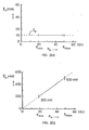
- Figures 2(a) and 2(b) illustrate an example of biasing conditions for an MR head for different sensor resistances R H for a conventional constant bias current I B scheme. If I B in Figure 2(a) is 10 mA, for example. Figure 2(b) shows that the head bias voltage V H varies accordingly between 200 mV and 500 mv as R H varies between 20 and 50 Ohms.
- Figures 2(c) and 2(d) illustrate exemplary bias conditions for an MR head for different sensor resistances R H for a conventional constant bias voltage V H scheme. If the bias voltage V B appearing across the sensor resistance R S in Figure 2(d) is 500 mv, for example, Figure 2(c) shows that the bias current I H through the MR head varies inversely proportional to the total head resistance R H .
- voltage biasing circuit that provides a constant bias voltage for an MR head.
- voltage biasing circuit includes a nulling circuit that adjusts the output of the voltage biasing circuit.
- the nulling circuit effectively increases the output of the voltage biasing circuit by an amount that is approximately equal to a cable drop across any parasitic cable resistances that are present.
- the Cahalan circuit uses a resistive element having a resistance that is an estimate of the parasitic cable resistance for generating the nulling voltage. This approach, however, does not compensate for any voltage drop appearing across the back-leads inside an MR head.
- the bias current through the MR head is adjusted during manufacturing to be inversely proportional to the MR head resistance R H , achieving an essentially constant MR head bias voltage.
- the resistance R H must be measured during the manufacturing process.
- None of these conventional MR head biasing scheme compensate for variations in physical characteristics of the MR head that occur during the manufacturing process, specifically, the sensor dimension tolerances. Consequently, operation of an MR head biased by a conventional biasing scheme is typically not at or near the operational optimum for the head. Further, uniform magnetic performance from MR head to MR head of a product, that is, less variability in magnetic performance from head to head regardless of manufacturing tolerances, is not typically achieved.
- US-A-5404102 discloses a biasing circuit for a magnetoresistive transducer in which a reference voltage is generated and compared with the voltage across the transducer to generate a feedback signal which is passed via a limiter to control a current source. This enables the current through the transducer to be limited to a predetermined maximum current and below that maximum the current is controlled to control the voltage drop across the transducer.
- JP-A-01-014702 discloses a bias circuit for a magnetoresistive transducer in which the current is controlled to compensate for abrasion wear of the transducer.
- the present invention allows for operation of an MR head at or closer to the operational optimum of the MR sensor, and achieves a more uniform magnetic performance from sensor to sensor regardless of physical variations within manufacturing tolerances than conventional biasing schemes.
- the MR sensor biasing schemes of the invention to be used in conjunction with a signal current sensing (low input impedance) readback amplifier (
- one embodiment of the present invention provides a bias circuit that generates a bias current I B and a bias voltage V H for a magnetoresistive (MR) transducer.
- the bias voltage V H is a voltage produced by the bias current I B flowing through a total resistance R H of the MR transducer, where the total resistance R H is the sum of a sensor resistance R S , a total head lead resistance R L , and a total front-lead resistance R f .
- This embodiment of the present invention includes a multiplier, a comparator, a controller and a currentgenerator.
- the multiplier has first and second inputs in which the first input receives a first signal that is related to the bias current I B and the second input receives a second signal that is related to the bias voltage V H .
- the multiplier generates a product signal that is proportional to a product of the first and second signals.
- the comparator compares the product signal to a reference signal that is proportional to a predetermined bias power P B dissipated by the MR transducer, and generates a control signal.
- the controller is responsive to the control signal by controlling one of the bias current I B and the bias voltage V H or both I B and V H , and as a result controls the bias power P B dissipated by the MR transducer to a predetermined value.
- the controller is responsive to the control signal by controlling the current generator to generate the bias current I B .
- the multiplier includes a current sink circuit and a differential amplifier.
- An input of the current sink circuit receives the second signal and, in response, the current sink circuit generates an output current that is proportional to the bias voltage V H .
- the differential amplifier has an input and an output, and is biased by the output current of the current sink circuit.
- the differential amplifier input receives the first signal and the differential amplifier output is therefore proportional to a product of the bias current I B and the bias voltage V H .
- the current sink circuit includes a first transistor having first, second and third nodes, and a first resistor.
- the second signal is coupled to the first node of the first transistor.
- the first resistor is coupled between the second node of the first transistor and a first power supply node.
- the differential amplifier includes second and third transistors, and second and third resistors.
- the second and third transistors each have first, second and third nodes, where the first signal is coupled between the first node of each of the second and third transistors.
- the second node of each of the second and third transistors are coupled to the third node of the first transistor.
- the second resistor is coupled between the third node of the second transistor and the second power supply node, while the third resistor is coupled between the third node of the third transistor and the second power supply node.
- the output of the differential amplifier appears between the third node of the second transistor and the third node of the third transistor.
- the comparator is an adder circuit coupled to the third node of the second transistor and the third node of the third transistor.
- the adder circuit adds to the output of the differential amplifier a predetermined current signal that is related to the reference signal.
- the biasing circuit includes a transducer equivalent circuit, a difference sensing circuit, and first and second current sources.
- the transducer equivalent circuit includes a voltage source and an input resistance.
- the voltage source has a predetermined voltage and the input resistance has a resistance that is related to the lead resistance R L of the MR transducer.
- the difference sensing circuit has first and second inputs, with the first input being coupled to the MR transducer and the second input being coupled to the transducer equivalent circuit.
- the difference sensing circuit senses a voltage difference between the first and second inputs.
- the first current source is responsive to the difference sensing circuit by generating a bias current I B for the MR transducer.
- the second current source is responsive to the difference sensing circuit by generating a control current that is coupled to the transducer equivalent circuit.
- the control current is proportional to the MR transducer bias current I B so that the predetermined voltage of the voltage source equals a predetermined voltage V B appearing across the sensor resistance R S in series with the front lead resistance R f .
- the difference sensing circuit includes first and second transistors each having first, second and third nodes.
- the first node of first transistor is coupled to the first and third nodes of the second transistor.
- the second node of the first transistor is coupled to the MR transducer.
- the second node of the second transistor is coupled to the transducer equivalent circuit.
- the first current source includes a third transistor having first, second and third nodes.
- the second current source includes a fourth transistor having first, second and third nodes. The first and third nodes of the third transistor are coupled to the first node of the fourth transistor to form a current mirror.
- the third node of the third transistor is coupled to the third node of the first transistor, and the third node of the fourth transistor is coupled to the third node of the second transistor.
- an area ratio of the first transistor to the second transistor is preferably N:1 and, similarly, an area ratio of the third transistor to the fourth transistor is preferably N:1.
- the first current source includes a first transistor having first, second and third nodes, and, likewise, the second current source includes a second transistor having first, second and third nodes.
- the first node of the first transistor and the first node of the second transistor are each coupled to an output of the difference sensing circuit.
- the third node of the first transistor is coupled to the MR transducer, and the third node of the second transistor is coupled to the MR transducer equivalent circuit.
- the biasing circuit of this embodiment also includes an output circuit that has first and second input nodes and an output node. The first input node of the output circuit is coupled to the third node of the first transistor and the second input node of the output circuit is coupled to the third node of the second transistor.
- the difference sensing circuit includes first and second transistors each having first, second and third nodes.
- the first node of first transistor is coupled to the first and third nodes of the second transistor.
- the second node of the first transistor is coupled to the MR transducer and the second node of the second transistor is coupled to the transducer equivalent circuit.
- the first current source includes third and fourth transistors each having first, second and third nodes.
- the second node of each of the third and fourth transistors are coupled to the third node of the first transistor.
- the second current source includes a fifth transistor having first, second and third nodes.
- the first node of the third transistor is coupled to the first and third node of the fifth transistor to form a current mirror, while the second node of the fifth transistor is coupled to the third node of the second transistor.
- an area ratio of the first transistor to the second transistor is N:1
- a current ratio of current flowing in the second node of the fourth transistor to the current flowing in the second node of the third transistor to the current flowing in the second node of the fifth transistor K:L:1, where K + L equals N.
- Still another configuration of the second embodiment includes a current sensing circuit and a third current source.
- the current sensing circuit senses the bias current I B generated by the first current source for the predetermined bias voltage V S appearing across the sensor resistance R S .
- the third current source is responsive to the current sensing circuit by generating an output current when the bias current I B generated by the first current source for the predetermined bias voltage V S is less than a predetermined sensor bias current.
- the output current generated by the third current source is coupled to the transducer equivalent circuit and combined with the control current generated by the second current source to form a combined control current.
- the combined control current is related to the MR transducer bias current I B such that a predetermined MR transducer bias current I B flows through the sensor resistance R S producing a predetermined effective magnetic bias of the sensor resistance R S .
- the difference sensing circuit includes first and second transistors each having first, second and third nodes.
- the first node of first transistor is coupled to the first and third nodes of the second transistor.
- the second node of the first transistor is coupled to the MR transducer, and the second node of the second transistor is coupled to the transducer equivalent circuit.
- the first current source includes a third transistor having first, second and third nodes, and the second current source includes a fourth transistor having first, second and third nodes.
- the first and third nodes of the third transistor is coupled to the first node of the fourth transistor to form a current mirror.
- the third node of the third transistor is coupled to the third node of the first transistor, and the third node of the fourth transistor is coupled to the third node of the second transistor.
- the current sensing circuit includes a fifth transistor, a fourth current source, and an amplifier circuit.
- the fifth transistor has first, second and third nodes, with the first node being coupled to the third node.
- the fourth current source is coupled to the third node of the fifth transistor.
- the amplifier circuit has a first input, a second input and an output. The first input of the amplifier is coupled to the third node of the third transistor. The second input is coupled to the third node of the fifth transistor and the amplifier output is coupled to the third current source.
- a third embodiment provides a circuit for magnetically biasing a magnetoresistive (MR) transducer.
- the biasing circuit includes a transducer equivalent circuit, a difference sensing circuit, and first and second current sources.
- the difference sensing circuit has first and second inputs, with the first input being coupled to the MR transducer and the second input being coupled to the transducer equivalent circuit.
- the difference sensing circuit senses a voltage difference between the first and second inputs.
- the first current source is responsive to the difference sensing circuit by generating a bias current I B for the MR transducer.
- the second current source is responsive to the difference sensing circuit by generating a control current that is coupled to the transducer equivalent circuit.
- the control current is proportional to the MR transducer bias current I B so that the bias current I B through the MR transducer produces a predetermined effective magnetic bias of a sensor portion of the MR transducer.
- the biasing circuit also includes a current sensing circuit and a third current source.
- the current sensing circuit senses the bias current I B generated by the first current source for the predetermined effective magnetic bias of the sensor portion of the MR transducer.
- the third current source is responsive to the current sensing circuit by generating an output current when the bias current I B generated by the first current source for the predetermined effective magnetic bias of the sensor portion of the MR transducer is less than a predetermined sensor bias current.
- the output current generated by the third current source is then coupled to the transducer equivalent circuit and combined with the control current generated by the second current source to form a combined control current.
- the combined control current is related to the MR transducer bias current I B so that a predetermined MR transducer bias current I B flows through the MR transducer producing the predetermined effective magnetic bias of the sensor portion of the MR transducer.
- the difference sensing circuit includes first and second transistors each having first, second and third nodes.
- the first node of the first transistor is coupled to the first and third nodes of the second transistor.
- the second node of the first transistor is coupled to the MR transducer, and the second node of the second transistor being coupled to the transducer equivalent circuit.
- the first current source includes a third transistor having first, second and third nodes.
- the second current source includes a fourth transistor having first, second and third nodes.
- the first and third nodes of the third transistor are coupled to the first node of the fourth transistor forming a current mirror.
- the third node of the third transistor is coupled to the third node of the first transistor.
- the third node of the fourth transistor is coupled to the third node of the second transistor.
- the current sensing circuit includes a fifth transistor, a fourth current source and an amplifier circuit.
- the fifth transistor has first, second and third nodes, with the first node being coupled to the third node.
- the fourth current source is coupled to the third node of the fifth transistor.
- the amplifier circuit has a first input, a second input and an output. The first input is coupled to the third node of the third transistor. The second input is coupled to the third node of the fifth transistor.
- the amplifier output is coupled to the third current source.
- the biasing circuits of the present invention can be part of an MR/AE circuit which is part of a disk drive.
- the present invention provides an MR head biasing scheme that compensates for physical variations from head to head within manufacturing tolerances of the head using one of five related approaches.
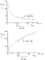
- Figures 3(a) and 3(b) show exemplary bias conditions for varying total head resistance R H for a constant bias power P B approach according to the invention.
- Figure 3(a) shows variations in head current I H for variations in total head resistance R H for a constant bias P B .
- Figure 3(b) shows corresponding variations in voltage across the head V H for variations in total head resistance R H for the same constant bias P B .
- An advantage of a constant bias power scheme over a conventional constant bias voltage approach is that increases in head current I H caused by larger sensor heights are less dramatic with a constant bias power scheme.
- a constant power biasing technique is useful for avoiding magnetic underbiasing of low sensor height heads (high R H ) due to a sensor demagnetization effect. This is because the head voltage V H does not remain constant for constant P B bias, but increases slightly for higher resistance heads.
- a second biasing approach is a constant MR sensor current density scheme.
- the current density J S in the MR sensor is held constant. This allows operation of all MR sensors in a product as close as possible to the electro-migration limits.
- the sensor cools by heat diffusing away from the sensor through the two-side surfaces facing the shields.
- the thermal resistance resulting from this facial cooling is inversely proportional to the sensor height h.
- Another cooling mechanism is by heat diffusion into the leads of the sensor.
- the thermal resistance associated with this cooling mechanism is also inversely proportional to the sensor height h.
- the total thermal resistance R thermal in equation (9) is inversely proportional to the sensor height h.
- a third biasing approach provides a constant MR sensor bias voltage V S .
- V S across the sensor that is the portion of the MR head corresponding to resistance R S and responsive to the magnetic data, is held constant for all MR heads in a product.
- a fourth MR sensor biasing approach is a constant MR sensor temperature rise bias scheme.
- This MR sensor biasing technique leads to the same sensor temperature rise (resulting from the electrical bias power dissipation in the sensor) of all heads in a product.
- this biasing approach is the same as the two previous biasing approaches. Since constant sensor temperature rise biasing, constant sensor current density biasing, and constant sensor bias voltage biasing are all independent of sensor height h, these three biasing approaches can all be treated as the same case.
- Figure 4(a) shows a schematic block diagram of an MR head, an AE module and wires w connected between the MR head and AE module.
- Figure 4(b) shows an equivalent circuit for an MR head with leads and wires. The MR head "sees" a bias voltage source having a negative input resistance at the input terminals of the AE module.
- Figure 4(c) shows an equivalent bias circuit where a voltage V S is developed across the sensor resistance R S of the MR sensor.
- Figure 4(d) shows an equivalent bias circuit where a voltage V B is developed across the sensor resistance R S and the lead front-end resistance R f .
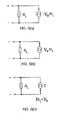
- Figures 5(a)-5(c) are equivalent circuit models for the circuit of Figure 4(d).
- Figures 6(a) and 6(b) show exemplary biasing conditions for a constant sensor temperature rise biasing scheme.
- sensor current I H is shown for varying total MR head resistance R H for a constant sensor temperature rise biasing.
- Figure 6(b) shows a graph of head bias voltage V H for varying MR head resistance R H for the same conditions.
- Figure 7(a) shows a theoretical curve for S s .
- Figures 7(b) and 7(c) show biasing conditions providing a practical approximation for a constant current density J S biasing according to the fifth biasing scheme of the present invention.
- a head resistance R HS corresponding to a sensor height h 0
- a head is biased with a constant bias voltage yielding a constant current density J S .
- a head is biased with a constant current I B , resulting in an increase in a sensor current density that is inversely proportional to the sensor height h and is proportional to the sensor resistance R S .
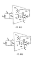
- FIGS 8(a) and 8(b) show schematic block diagrams for illustrating the general concept of the constant MR head power biasing scheme according to the present invention.
- Each electronic circuit shown in Figures 8(a) and 8(b) includes a multiplying device 81, for example, a well-known transconductance multiplier having a first input signal that is proportional to I B and a second input signal that is proportional to V H .
- I B and V S are signals available at the input terminals of an AE module.
- the product signal output 82 from multiplier 81 is compared by a comparator 83 to a reference signal 84.
- Signal 84 is proportional to the desired bias power P B dissipated by MR head resistance R H .
- Comparator 83 outputs a control signal 85 that is proportional to the difference of the product signal 82 and reference signal 84 and is used for controlling the bias current I B ( Figure 8(a)) or for controlling the head voltage V H ( Figure. 8(b)) such that the product I B V H is constant.
- the head resistance R H need not be a known value, that is, it may vary from head to head.
- the controlled variable is V H and the variable I B is linked to V H .
- FIG. 9 shows a schematic block diagram of a bias circuit 800 that provides a constant bias power to an MR head.
- Bias circuit 900 includes a current sink formed by amplifier 901, transistor 902 and resistor 903. The output current of the current sink is proportional to head voltage V R .
- the output of amplifier 901 is coupled to the base of transistor 902.
- the emitter of transistor 902 is coupled to the inverting input of amplifier 901 and to a first power source V S1 through resistor 903.
- the non-inverting input of amplifier 901 is connected to input terminal 904 of bias circuit 900.
- Input terminal 905 of circuit 900 is coupled to power source V S1 .
- MR head (R H ) is connected across input terminals 904 and 905.
- the magnitude of the voltage V S appearing across R H is connected across the current sink and controls the magnitude of the collector current of transistor 902.
- Transistors 906 and 907 are connected to form a first differential amplifier. That is, the emitters of transistors 906 and 907 are connected together and coupled to the collector of transistor 902. The bases of transistors 906 and 907 are coupled to opposite sides of a resistor 917. Resistor 917 is connected so that the current flowing through resistor 917 is the bias current I B that flows through terminal 904 and through R H . The collector of transistor 906 is connected to a second power source V S2 through resistor 908, while the collector of transistor 907 is connected to second power source V S2 through resistor 909. The differential collector current of transistors 906 and 907 is proportional to I B V H .
- a second differential amplifier is formed by transistors 910 and 911, and current source 913.
- the emitters of transistors 910 and 911 are connected together and coupled to one terminal of current source 913.
- the other terminal of current source 913 is connected to first power source V S1 .
- Current source 913 outputs current I B that is used for biasing transistors 910 and 911.
- the collector of transistor 910 is coupled to the collector of transistor 906, and the collector of transistor 911 is coupled to the collector of transistor 907.
- a reference voltage V ref which has a magnitude that is proportional to the desired bias power P B , is applied between the bases of transistors 910 and 911 causing a constant differential current at the collectors of transistors 910 and 911 to be subtracted from the differential current output of transistors 906 and 907.
- the constant amount can be varied by varying V ref
- Figure 9 shows that V ref is externally applied to circuit 900, V ref can alternatively be made to have a constant magnitude, that is, internal to circuit 900, and I B can be made to be varied externally in proportion to the desired bias power P B for accommodating a wide range of products having different P B requirements.
- the collector of transistor 906 is coupled to the inverting input to a control amplifier 914, and the collector of transistor 907 is coupled to the non-inverting input of control amplifier 914.
- the output of amplifier 914 controls a current source formed by transistor 916 and resistor 915.
- Transistor 916 and resistor 915 generate bias current I B that flows through resistor 917 and through head resistance R H .
- R L , and R S are the resistance of resistors 903 and 917, respectively.
- a constant sensor biasing can be implemented by compensating for the non-sensor resistance part of the head resistance, that is, the lead resistance R L and the front-lead resistance R f , or more easily by compensating only for the lead resistance R L (see Figure 4(d)).
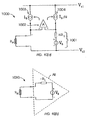
- Figures 10(a) and 10(b) show a schematic block diagram of a circuit 1000 providing a constant sensor voltage bias and Figure 10(b) shows a network equivalent circuit 1010 for the schematic block diagram of Figure 10(a).
- Circuit 1000 includes an amplifier 1002 that senses a voltage difference between the total head resistance R H and the model or equivalent circuit 1001 for the MR transducer, that is, a circuit having a NR L in series.
- Amplifier 1002 adjusts two current sources 1003 and 1004 until the voltage difference sensed at the input to amplifier 1002 equals zero.
- current source 1003 supplies current I B
- current source 1004 supplies current I B /N, where N is chosen to be greater than 1 for power savings considerations. However, N may be chosen other considerations in mind. Practical values for N are in the range from 5-20.
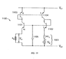
- Figure 11 shows a schematic block diagram of a circuit 1100 providing a constant voltage V B across the sensor resistance R S portion of an MR head.
- Circuit 1100 includes a transistor 1101 connected as an emitter follower. The base-emitter voltage of transistor 1101 is cancelled by the base-emitter voltage of transistor 1102, which has an area preferably N times smaller than T, transistor 1101 for power saving considerations.
- the resistance NR, of equivalent circuit 1001 is scaled accordingly by N.
- Transistor 1101 is preferably the input transistor of the readback amplifier of an AE module. Although not shown in Figure 11, the readback signal is detected at the collector of transistor 1101.
- Capacitor 1105 is connected between the bases of transistors 1101 and 1102 and power source V S2 for providing filtering.
- NR L and V B can be provided off-chip for greater flexibility.
- a current mirror is formed by transistors 1103 and 1104, and is connected in any well-known current mirror configuration (double FET mirror, etc.), and is also scaled by a factor N. This current mirror forces the currents through transistors 1101 and 1102, and also through R H and model 1001 to be scaled by N.
- Figure 12 shows a schematic block diagram of another circuit 1200 providing a constant voltage V B across the sensor resistance R S portion of an MR head.
- Circuit 1200 is configured for detecting an MR head readback signal directly from the MR head signal voltage.
- Circuit 1200 includes MR equivalent circuit 1001.
- Amplifier 1201 is connected to detect a voltage difference between the voltage V H appearing across the MR head and the voltage appearing across equivalent circuit 1001.
- the non-inverting input of amplifier 1201 is coupled to the MR head, while the inverting input of amplifier 1201 is coupled to the equivalent circuit 1001.
- the output of amplifier 1201 is connected to the bases of transistors 1202 and 1204, which are both configured as controllable current sources.
- Capacitor 1206 is coupled between the output of amplifier 1201 and a power supply voltage V S2 for providing filtering of the control signal output from amplifier 1201.
- the emitter of transistor 1202 is coupled to power supply voltage V S2 through resistor 1203. Similarly, the emitter of transistor 1204 is coupled to supply voltage V S2 through resistor 1205.
- the collector of transistor 1202 is coupled to the MR head, while the collector of transistor 1204 is coupled to equivalent circuit 1001 through diodes 1208 and 1209. Capacitor 1207 is connected to the collector of transistor 1204 for filtering purposes.
- Circuit 1200 includes an output stage formed by transistors 1211 and 1212.
- the base of transistor 1212 is coupled to the collector of transistor 1202.
- the base of transistor 1211 is coupled to the collector of transistor 1204.
- the collector of transistor 1211 is coupled to power supply V S2 through resistor 1210.
- the detected readback signal from the MR head is generated across resistor 1210 between terminals 1213 and 1214.
- FIG. 13 shows a schematic block diagram of an input stage circuit 1300 for a single-ended MR preamplifier using sensor biasing.
- Circuit 1300 includes circuit 1100 that is shown in Figure 11. Additionally, a current source 1304 having a current I comp equal to 2I B / ⁇ , where ⁇ is the current gain of transistor 1103, is connected between a voltage source V S2 (+5 v for example) and the bases of transistors 1103 and 1104.
- a current source containing an amplifier 1305, a capacitor 1306, a compensation diode 1307, a resistor 1308 and a transistor 1309 is used for "bleeding off" part of the bias current I B around resistor 1303, so that resistor 1303 can have a larger resistive value, for example, 450 Ohms, for providing more gain without causing transistor head-room problems.
- resistor 1308 should preferably have a resistive value of 194 Ohms so that 70% of I B is sourced through transistor 1309.
- capacitor 1306 is 470 pF.
- a series diode 1301 (self-biased transistor) is used with transistor 1302. This circuit configuration, however, can result in signal distortion, offset, etc., despite compensation diode 1307 in the bleed-off current source.
- Circuit 1400 is an input stage of a single-ended MR preamplifier using sensor biasing, and includes circuit 1100 ( Figure 11), and the bleed-off current source (circuit 1300).
- circuit 1400 includes circuit 1100 ( Figure 11), and the bleed-off current source (circuit 1300).
- diodes 1301 and 1307 of circuit 1300 have been eliminated.
- Resistors 1303 and 1308 are chosen to be equal, for example, 450 Ohms, so that 50% of I B flows through transistor 1103 and 50% flows through transistor 1309.
- An amplifier 1401 is coupled to the emitters of the current mirror formed by transistors 1103 and 1104.
- the output of amplifier 1401 is coupled to the gate of a transistor 1404.
- the source of transistor 1404 is coupled to voltage source V S2 through resistor 1403.
- the drain of transistor 1404 is coupled to the collector of transistor 1104.
- Capacitor 1402 is used for filtering purposes.
- the magnitude of the compensation current in the right-most vertical branch containing head equivalent circuit 1001 is derived from the base-emitter of the cascode transistor 1103 above input transistor 1101.
- Amplifier 1401 controls the FET current source, that is, transistor 1404, so that the compensation current in the right-most branch is 1/10 times, for example, the input bias current I B through the MR head.
- FIG. 15 shows a schematic block diagram of a circuit 1500 providing a constant effective magnetic bias according to the present invention.
- Circuit 1500 includes circuit 1100 of Figure 11.
- Circuit 1500 provides a constant sensor voltage for relatively low values of R H for which the head bias current through R H and transistor 1101 is sufficiently large to turn off a controllable current source formed by transistor 1502 and resistor 1503.
- the bias current I B becomes sufficiently small that amplifier 1501, which compares the voltage drop across transistor 1504 with the voltage drop across transistor 1103 (both shown connected as diodes), applies a forward voltage to the base of transistor 1502.
- Transistor turns on accordingly and circuit 1500 supplies a constant current bias to the MR head.
- Figures 16(a) and 16(b) show exemplary MR head biasing conditions for constant effective magnetic biasing circuit 1500. The cross-over point is determined by the value of the (reference) current I 0 and the transistor area ratio N.
- the bias current I B V B / ( R H - R L ) .
- All of the disclosed embodiments and configurations of the bias circuit of the present invention can be made part of circuitry in an MR/AE module which is part of a disk drive.
Landscapes
- Physics & Mathematics (AREA)
- Condensed Matter Physics & Semiconductors (AREA)
- General Physics & Mathematics (AREA)
- Engineering & Computer Science (AREA)
- Chemical & Material Sciences (AREA)
- Nanotechnology (AREA)
- Manufacturing & Machinery (AREA)
- Crystallography & Structural Chemistry (AREA)
- Magnetic Heads (AREA)
- Recording Or Reproducing By Magnetic Means (AREA)
- Measuring Magnetic Variables (AREA)
Description
- The present invention relates to magnetoresistive (MR) sensor biasing. More particularly, the present invention relates to magnetoresistive sensor biasing circuits.
- For the purpose of this disclosure, the terms "magnetoresistive (MR) sensor" and "MR head" both encompass any magnetoresistive element used for detecting a varying magnetic field by detecting a change in resistance ΔRS of the element resistance RS caused by variations in the magnetic field. Also for purposes of this disclosure, the terms MR sensor and MR head are both not limited to magnetic recording elements only. Examples of embodiments of MR sensors that are contemplated to be within the scope of these two terms include, but are not limited to, barber pole MRs, dual MRs, soft adjacent layer MRs, differential MRs, spin valve MRs, tunnel junction MRs and giant MRs.
- An MR sensor is an energetically passive sensor that uses a sense current (or voltage) for detecting a change in sensor resistance in the form of a signal voltage or signal current. The sense current may also be used for providing all or part of a magnetic bias for the sensor that is needed for proper MR sensor operation. This disclosure does not distinguish between sense and bias current (or voltage). The terms (MR sensor) bias current and voltage are used interchangeably throughout this disclosure. The biasing and readout electronics associated with an MR sensor are generally referred to as an arm electronic (AE) module.
- The physical characteristics of an MR sensor are determined by the properties of the materials used, the MR sensor sandwich configuration, and the sensor dimensions, that is, the thickness, height and length of the sensor. The dimension having the greatest tolerance in externally exposed MR sensors used for magnetic recording is the sensor height h. The tolerance on this dimension is for compensating for head wear and lapping for tape heads, and for ABS lapping for disk drive heads.
- Figure 1(a) shows the physical relationships between the different resistances forming the total MR head resistance RS. Figure 1(b) shows a schematic diagram for an electrical model of resistance RH. The total MR head resistance RH is measured at
terminals 10 and 11 of the AE module. The MR head and the AE module are shown as part of a disk drive 12 in Figure 1(a). The portion of the total MR head resistance that varies in accordance with a varying magnetic field is the sensor resistance RS, with the resulting change in resistance being indicated as ΔRS.
Resistance RS varies inversely proportional to the sensor height h. The total head lead resistance RL is the resistance of the wires to the preamplifier of the AE module and the resistance of the back-leads BL inside the MR head. Lastly, the total front-lead resistance of the MR head is indicated as Rf. Resistance Rf also varies inversely proportional to the sensor height h. However, Rf shows no signal variations for varying magnetic field. Equations (1) · (4) represent these principles in symbolic notation.


- In Figures 1(a) and 1(b) and throughout the following disclosure, bias current Ia equals head bias current IH. The voltage VH is the bias voltage appearing across the total MR head resistance RH. voltage VB is the bias voltage appearing across sensor resistance RS and front lead resistance Rf. voltage VS is the bias voltage appearing across sensor resistance RS. Height h is the physical height of the sensor.
- There are three conventional approaches for providing MR sensor biasing: a constant bias current scheme; a constant bias voltage scheme; and an adjusted bias current scheme for attaining constant bias voltage. The term "constant" as used when referring to biasing schemes indicates a biasing invariability from sensor to sensor in view of manufacturing tolerances. For a conventional constant bias current scheme, the same bias/sense DC current is applied to all MR heads by AE modules during manufacturing of a product regardless of the respective head resistances, sensor heights, etc., of the MR heads. Figures 2(a) and 2(b) illustrate an example of biasing conditions for an MR head for different sensor resistances RH for a conventional constant bias current IB scheme. If IB in Figure 2(a) is 10 mA, for example. Figure 2(b) shows that the head bias voltage VH varies accordingly between 200 mV and 500 mv as RH varies between 20 and 50 Ohms.
- For a conventional constant bias voltage scheme, the same bias/sense DC voltage is applied to all MR heads in a product by an AE module. Figures 2(c) and 2(d) illustrate exemplary bias conditions for an MR head for different sensor resistances RH for a conventional constant bias voltage VH scheme. If the bias voltage VB appearing across the sensor resistance RS in Figure 2(d) is 500 mv, for example, Figure 2(c) shows that the bias current IH through the MR head varies inversely proportional to the total head resistance RH.
- U.S. 5,309,294 to Cahalan, issued May 3, 1994, discloses voltage biasing circuit that provides a constant bias voltage for an MR head. According to Cahalan, voltage biasing circuit includes a nulling circuit that adjusts the output of the voltage biasing circuit. The nulling circuit effectively increases the output of the voltage biasing circuit by an amount that is approximately equal to a cable drop across any parasitic cable resistances that are present. The Cahalan circuit uses a resistive element having a resistance that is an estimate of the parasitic cable resistance for generating the nulling voltage. This approach, however, does not compensate for any voltage drop appearing across the back-leads inside an MR head.
- In the conventional adjusted bias current scheme for attaining a constant bias voltage, the bias current through the MR head is adjusted during manufacturing to be inversely proportional to the MR head resistance RH, achieving an essentially constant MR head bias voltage. The resistance RH must be measured during the manufacturing process.
- None of these conventional MR head biasing scheme compensate for variations in physical characteristics of the MR head that occur during the manufacturing process, specifically, the sensor dimension tolerances. Consequently, operation of an MR head biased by a conventional biasing scheme is typically not at or near the operational optimum for the head. Further, uniform magnetic performance from MR head to MR head of a product, that is, less variability in magnetic performance from head to head regardless of manufacturing tolerances, is not typically achieved.
- US-A-5404102 discloses a biasing circuit for a magnetoresistive transducer in which a reference voltage is generated and compared with the voltage across the transducer to generate a feedback signal which is passed via a limiter to control a current source. This enables the current through the transducer to be limited to a predetermined maximum current and below that maximum the current is controlled to control the voltage drop across the transducer.
- In an article entitled "Adaptive Compensator" by J.M. Harp et al published in IBM Technical Disclosure Bulletin, Vol. 27, No. 1A of June 1984, the biasing of magnetoresistive is discussed, and a circuit is proposed which enables the user to control the bias current. The intention is for the current to be controlled to a stable operating point.
- JP-A-01-014702 discloses a bias circuit for a magnetoresistive transducer in which the current is controlled to compensate for abrasion wear of the transducer.
- The invention is defined by the independent claim.
- It is an object of the present invention to provide an MR head biasing scheme that generally allows for variations in the physical characteristics of an MR sensor occurring during manufacturing, specifically for the physical tolerances of the head occurring during manufacturing. In this regard, the present invention allows for operation of an MR head at or closer to the operational optimum of the MR sensor, and achieves a more uniform magnetic performance from sensor to sensor regardless of physical variations within manufacturing tolerances than conventional biasing schemes.
- It is another object of the present invention to provide a sensor biasing scheme that does not rely on head resistance RH measurements. Consequently, it is an object of the present invention to make use of a "head model" that is based on the head lead resistance RL and the bias voltage VB appearing across the sensor resistance RS portion of the total head resistance RH that is inversely proportional to the sensor height h and that is varying with the magnetic data signal. Additionally, it is an object of the present invention to use a controlled current source to achieve constant current density JS in an MR sensor and a constant temperature rise of an MR sensor, regardless of sensor height h. Consequently, maximum allowable bias is provided for all heads in a product with respect to limits set in accordance with electromigration and interdiffusion. It is an object of the present invention for the MR sensor biasing schemes of the invention to be used in conjunction with a signal current sensing (low input impedance) readback amplifier (|zin| < RH), as well as with a signal voltage sensing high input impedance readback amplifier (|Zin| > RH).
- Different aspects of the invention are disclosed in the dependent claims.
- To achieve these and other objects, one embodiment of the present invention provides a bias circuit that generates a bias current IB and a bias voltage VH for a magnetoresistive (MR) transducer. The bias voltage VH is a voltage produced by the bias current IB flowing through a total resistance RH of the MR transducer, where the total resistance RH is the sum of a sensor resistance RS, a total head lead resistance RL, and a total front-lead resistance Rf. This embodiment of the present invention includes a multiplier, a comparator, a controller and a currentgenerator. The multiplier has first and second inputs in which the first input receives a first signal that is related to the bias current IB and the second input receives a second signal that is related to the bias voltage VH. The multiplier generates a product signal that is proportional to a product of the first and second signals. The comparator compares the product signal to a reference signal that is proportional to a predetermined bias power PB dissipated by the MR transducer, and generates a control signal. The controller is responsive to the control signal by controlling one of the bias current IB and the bias voltage VH or both IB and VH, and as a result controls the bias power PB dissipated by the MR transducer to a predetermined value. Preferably, the controller is responsive to the control signal by controlling the current generator to generate the bias current IB.
- According to the invention, the multiplier includes a current sink circuit and a differential amplifier. An input of the current sink circuit receives the second signal and, in response, the current sink circuit generates an output current that is proportional to the bias voltage VH. The differential amplifier has an input and an output, and is biased by the output current of the current sink circuit. The differential amplifier input receives the first signal and the differential amplifier output is therefore proportional to a product of the bias current IB and the bias voltage VH. More specifically, the current sink circuit includes a first transistor having first, second and third nodes, and a first resistor. The second signal is coupled to the first node of the first transistor. The first resistor is coupled between the second node of the first transistor and a first power supply node. The differential amplifier includes second and third transistors, and second and third resistors. The second and third transistors each have first, second and third nodes, where the first signal is coupled between the first node of each of the second and third transistors. The second node of each of the second and third transistors are coupled to the third node of the first transistor. The second resistor is coupled between the third node of the second transistor and the second power supply node, while the third resistor is coupled between the third node of the third transistor and the second power supply node. The output of the differential amplifier appears between the third node of the second transistor and the third node of the third transistor. Preferably, the comparator is an adder circuit coupled to the third node of the second transistor and the third node of the third transistor. The adder circuit adds to the output of the differential amplifier a predetermined current signal that is related to the reference signal.
- Another embodiment provides a biasing circuit for a magnetoresistive (MR) transducer, where the transducer is defined as having a total resistance RH. Resistance RH includes a sensor resistance RS, a lead resistance RL and a front-lead resistance Rf. The biasing circuit includes a transducer equivalent circuit, a difference sensing circuit, and first and second current sources. The transducer equivalent circuit includes a voltage source and an input resistance. The voltage source has a predetermined voltage and the input resistance has a resistance that is related to the lead resistance RL of the MR transducer. The difference sensing circuit has first and second inputs, with the first input being coupled to the MR transducer and the second input being coupled to the transducer equivalent circuit. The difference sensing circuit senses a voltage difference between the first and second inputs. The first current source is responsive to the difference sensing circuit by generating a bias current IB for the MR transducer. Similarly, the second current source is responsive to the difference sensing circuit by generating a control current that is coupled to the transducer equivalent circuit. According to the invention, the control current is proportional to the MR transducer bias current IB so that the predetermined voltage of the voltage source equals a predetermined voltage VB appearing across the sensor resistance RS in series with the front lead resistance Rf.
- Since both RS and Rf are inversely proportional to the sensor height h, the constant voltage appearing across RS and Rf also provides a constant (i.e. sensor height independent) voltage across RS.
- In one configuration of the second embodiment, the difference sensing circuit includes first and second transistors each having first, second and third nodes. The first node of first transistor is coupled to the first and third nodes of the second transistor. The second node of the first transistor is coupled to the MR transducer. The second node of the second transistor is coupled to the transducer equivalent circuit. The first current source includes a third transistor having first, second and third nodes. Similarly, the second current source includes a fourth transistor having first, second and third nodes. The first and third nodes of the third transistor are coupled to the first node of the fourth transistor to form a current mirror. The third node of the third transistor is coupled to the third node of the first transistor, and the third node of the fourth transistor is coupled to the third node of the second transistor. For power considerations, an area ratio of the first transistor to the second transistor is preferably N:1 and, similarly, an area ratio of the third transistor to the fourth transistor is preferably N:1.
- In another configuration of the second embodiment, the first current source includes a first transistor having first, second and third nodes, and, likewise, the second current source includes a second transistor having first, second and third nodes. The first node of the first transistor and the first node of the second transistor are each coupled to an output of the difference sensing circuit. The third node of the first transistor is coupled to the MR transducer, and the third node of the second transistor is coupled to the MR transducer equivalent circuit. The biasing circuit of this embodiment also includes an output circuit that has first and second input nodes and an output node. The first input node of the output circuit is coupled to the third node of the first transistor and the second input node of the output circuit is coupled to the third node of the second transistor.
- In yet another configuration of the second embodiment, the difference sensing circuit includes first and second transistors each having first, second and third nodes. The first node of first transistor is coupled to the first and third nodes of the second transistor. The second node of the first transistor is coupled to the MR transducer and the second node of the second transistor is coupled to the transducer equivalent circuit. The first current source includes third and fourth transistors each having first, second and third nodes. The second node of each of the third and fourth transistors are coupled to the third node of the first transistor. The second current source includes a fifth transistor having first, second and third nodes. The first node of the third transistor is coupled to the first and third node of the fifth transistor to form a current mirror, while the second node of the fifth transistor is coupled to the third node of the second transistor. Preferably, an area ratio of the first transistor to the second transistor is N:1, and a current ratio of current flowing in the second node of the fourth transistor to the current flowing in the second node of the third transistor to the current flowing in the second node of the fifth transistor K:L:1, where K + L equals N.
- Still another configuration of the second embodiment includes a current sensing circuit and a third current source. The current sensing circuit senses the bias current IB generated by the first current source for the predetermined bias voltage VS appearing across the sensor resistance RS. The third current source is responsive to the current sensing circuit by generating an output current when the bias current IB generated by the first current source for the predetermined bias voltage VS is less than a predetermined sensor bias current. The output current generated by the third current source is coupled to the transducer equivalent circuit and combined with the control current generated by the second current source to form a combined control current. The combined control current is related to the MR transducer bias current IB such that a predetermined MR transducer bias current IB flows through the sensor resistance RS producing a predetermined effective magnetic bias of the sensor resistance RS.
- Preferably for this configuration, the difference sensing circuit includes first and second transistors each having first, second and third nodes. The first node of first transistor is coupled to the first and third nodes of the second transistor. The second node of the first transistor is coupled to the MR transducer, and the second node of the second transistor is coupled to the transducer equivalent circuit. The first current source includes a third transistor having first, second and third nodes, and the second current source includes a fourth transistor having first, second and third nodes. The first and third nodes of the third transistor is coupled to the first node of the fourth transistor to form a current mirror. The third node of the third transistor is coupled to the third node of the first transistor, and the third node of the fourth transistor is coupled to the third node of the second transistor.
- The current sensing circuit includes a fifth transistor, a fourth current source, and an amplifier circuit. The fifth transistor has first, second and third nodes, with the first node being coupled to the third node. The fourth current source is coupled to the third node of the fifth transistor. The amplifier circuit has a first input, a second input and an output. The first input of the amplifier is coupled to the third node of the third transistor. The second input is coupled to the third node of the fifth transistor and the amplifier output is coupled to the third current source.
- A third embodiment provides a circuit for magnetically biasing a magnetoresistive (MR) transducer. The biasing circuit includes a transducer equivalent circuit, a difference sensing circuit, and first and second current sources. The difference sensing circuit has first and second inputs, with the first input being coupled to the MR transducer and the second input being coupled to the transducer equivalent circuit. The difference sensing circuit senses a voltage difference between the first and second inputs. The first current source is responsive to the difference sensing circuit by generating a bias current IB for the MR transducer. The second current source is responsive to the difference sensing circuit by generating a control current that is coupled to the transducer equivalent circuit. The control current is proportional to the MR transducer bias current IB so that the bias current IB through the MR transducer produces a predetermined effective magnetic bias of a sensor portion of the MR transducer.
- The biasing circuit also includes a current sensing circuit and a third current source. The current sensing circuit senses the bias current IB generated by the first current source for the predetermined effective magnetic bias of the sensor portion of the MR transducer. The third current source is responsive to the current sensing circuit by generating an output current when the bias current IB generated by the first current source for the predetermined effective magnetic bias of the sensor portion of the MR transducer is less than a predetermined sensor bias current. The output current generated by the third current source is then coupled to the transducer equivalent circuit and combined with the control current generated by the second current source to form a combined control current. The combined control current is related to the MR transducer bias current IB so that a predetermined MR transducer bias current IB flows through the MR transducer producing the predetermined effective magnetic bias of the sensor portion of the MR transducer.
- Preferably, the difference sensing circuit includes first and second transistors each having first, second and third nodes. The first node of the first transistor is coupled to the first and third nodes of the second transistor. The second node of the first transistor is coupled to the MR transducer, and the second node of the second transistor being coupled to the transducer equivalent circuit. The first current source includes a third transistor having first, second and third nodes. Similarly, the second current source includes a fourth transistor having first, second and third nodes. The first and third nodes of the third transistor are coupled to the first node of the fourth transistor forming a current mirror. The third node of the third transistor is coupled to the third node of the first transistor. The third node of the fourth transistor is coupled to the third node of the second transistor.
- The current sensing circuit includes a fifth transistor, a fourth current source and an amplifier circuit. The fifth transistor has first, second and third nodes, with the first node being coupled to the third node. The fourth current source is coupled to the third node of the fifth transistor. The amplifier circuit has a first input, a second input and an output. The first input is coupled to the third node of the third transistor. The second input is coupled to the third node of the fifth transistor. The amplifier output is coupled to the third current source.
- The biasing circuits of the present invention can be part of an MR/AE circuit which is part of a disk drive.
- The invention will now be described by way of example only and with reference to the accompanying drawings, in which:
- Figure 1(a) shows the physical relationship between the different resistances forming the total MR head resistance RH;
- Figure 1(b) shows a schematic diagram for an electrical model of resistance RH;
- Figures 2(a) and 2(b) illustrate exemplary bias conditions for different sensor resistances RH for an MR head for a conventional constant bias current IB approach;
- Figures 2(c) and 2(d) illustrate exemplary bias conditions for different sensor resistances RH for an MR head for a conventional constant bias voltage VH approach;
- Figures 3(a) and 3(b) show exemplary bias conditions for varying sensor resistance RH for a constant bias power PB approach according to the present invention;
- Figure 4(a) shows a schematic block diagram of an MR head connected to an arm electronics module;
- Figure 4(b) shows an equivalent circuit for an MR head according to the present invention;
- Figures 4(c) and 4(d) show equivalent circuits according to the present invention for a bias voltage source VS having a negative input resistance;
- Figures 5(a)-5(c) show schematic block diagrams of equivalent circuits for the biasing circuit of Figure 4(d);
- Figures 6(a) and 6(b) show exemplary biasing conditions for an MR head for a constant sensor temperature rise biasing approach according to the present invention;
- Figure 7(a) shows theoretical biasing conditions for achieving a constant effective magnetic bias;
- Figures 7(b) and 7(c) show biasing conditions for a practical approximation for achieving a constant effect magnetic bias according to the present invention;
- Figures 8(a) and 8(b) show schematic block diagrams for illustrating the general concept of constant MR head power biasing according to the present invention;
- Figure 9 shows a schematic block diagram of a bias circuit providing a constant bias power circuit for an MR head according to the present invention;
- Figure 10(a) shows a schematic block diagram of a circuit providing a constant voltage bias for the sensor resistance of an MR head.
- Figure 10(b) shows a network equivalent circuit for the schematic block diagram of Figure 10(a);
- Figure 11 shows an alternative schematic block diagram of a circuit providing a constant voltage across the sensor resistance portion of an MR head;
- Figure 12 shows a schematic block diagram of another circuit providing a constant voltage across the sensor resistance portion of an MR head;
- Figure 13 shows a schematic block diagram of an input stage for a single-ended MR preamplifier circuit using sensor biasing;
- Figure 14 shows another schematic block diagram of an input stage of a single-ended MR preamplifier circuit using sensor biasing;
- Figure 15 shows a schematic block diagram of a circuit providing a constant effective magnetic bias for an MR head; and
- Figures 16(a) and 16(b) show head biasing conditions for a constant effective magnetic biasing.
- The present invention provides an MR head biasing scheme that compensates for physical variations from head to head within manufacturing tolerances of the head using one of five related approaches. The first approach is to electrically bias an MR head so that the (electrical) power dissipation in the head is kept constant from head to head, regardless of variations in total head resistance RH due to manufacturing tolerances. This is accomplished by keeping the product of the DC voltage across the head VH and the DC current through the head IH constant. That is,

- Figures 3(a) and 3(b) show exemplary bias conditions for varying total head resistance RH for a constant bias power PB approach according to the invention. Figure 3(a) shows variations in head current IH for variations in total head resistance RH for a constant bias PB. Figure 3(b) shows corresponding variations in voltage across the head VH for variations in total head resistance RH for the same constant bias PB. An advantage of a constant bias power scheme over a conventional constant bias voltage approach is that increases in head current IH caused by larger sensor heights are less dramatic with a constant bias power scheme. Additionally, a constant power biasing technique is useful for avoiding magnetic underbiasing of low sensor height heads (high RH) due to a sensor demagnetization effect. This is because the head voltage VH does not remain constant for constant PB bias, but increases slightly for higher resistance heads.
- A second biasing approach is a constant MR sensor current density scheme. With this bias technique, the current density JS in the MR sensor is held constant. This allows operation of all MR sensors in a product as close as possible to the electro-migration limits. The electro-migration depends on current density,

where ρ = sensor resistivity.
l = sensor length,
h = sensor height,
t = sensor thickness.
VS = the voltage across the sensor, that is, the portion of the MR head corresponding to resistance RS and responsive to the magnetic data, and
IS = the current through the sensor (which equals the current through the entire MR head IH). - The sensor resistance is given by

- The (electrical) power dissipation in the sensor is therefore

- The temperature rise ΔTS of the sensor due to the electrical power dissipation is

where Rthermal is the thermal resistance of the sensor to ambient. - The sensor cools by heat diffusing away from the sensor through the two-side surfaces facing the shields. The thermal resistance resulting from this facial cooling is inversely proportional to the sensor height h. Another cooling mechanism is by heat diffusion into the leads of the sensor. The thermal resistance associated with this cooling mechanism is also inversely proportional to the sensor height h. Hence, the total thermal resistance Rthermal in equation (9) is inversely proportional to the sensor height h.

where K is an arbitrary constant. Therefore,
is no longer a function of the sensor height h. Consequently, if the biasing circuitry of an MR sensor is designed to bias at a constant current density JS, all MR sensors in a product will be operating at the same temperature rise ΔTS above ambient. - A third biasing approach provides a constant MR sensor bias voltage VS. For this scheme, the voltage VS across the sensor, that is the portion of the MR head corresponding to resistance RS and responsive to the magnetic data, is held constant for all MR heads in a product.
- Rewriting equation (12) with:


- It also follows that for constant sensor voltage biasing, the sensor temperature rise is the same for all sensors in a product.
- With

the current density of the sensor JS is
- Hence, if VS is held constant for all heads within a product, JS is also held constant for heads within the same product. Thus, both the constant MR sensor current density bias scheme and the constant MR sensor bias voltage scheme are identical. It should be understood that constant voltage biasing of an MR sensor is not the same as conventional constant voltage biasing of an entire MR head, which does not produce the advantages of constant temperature rise and constant current density.
- A fourth MR sensor biasing approach is a constant MR sensor temperature rise bias scheme. This MR sensor biasing technique leads to the same sensor temperature rise (resulting from the electrical bias power dissipation in the sensor) of all heads in a product. Naturally, this biasing approach is the same as the two previous biasing approaches. Since constant sensor temperature rise biasing, constant sensor current density biasing, and constant sensor bias voltage biasing are all independent of sensor height h, these three biasing approaches can all be treated as the same case. Since

and
a constant voltage bias across the front-lead resistance Rf and the sensor resistance RS, that is across Rf + RS, will also produce a constant current density in the sensor and provide a constant temperature rise for all sensors in a product, regardless of sensor height h. Therefore, a constant sensor temperature rise can be obtained in principle as indicated by the schematic block diagrams of Figures 4(a)-4(d). - Figure 4(a) shows a schematic block diagram of an MR head, an AE module and wires w connected between the MR head and AE module. Figure 4(b) shows an equivalent circuit for an MR head with leads and wires. The MR head "sees" a bias voltage source having a negative input resistance at the input terminals of the AE module. Figure 4(c) shows an equivalent bias circuit where a voltage VS is developed across the sensor resistance RS of the MR sensor. Figure 4(d) shows an equivalent bias circuit where a voltage VB is developed across the sensor resistance RS and the lead front-end resistance Rf. The equivalent circuit shown in Figure 4(c), where the input resistance is -(Rf + RL), is relatively difficult to realize because Rf ∝ 1/h and is dependent on each individual head. RL, on the other hand, is relatively constant. Consequently, the equivalent circuit shown in Figure 4(d), having a bias voltage VB and an input resistance -RL, is the preferred implementation for a biasing circuit that provides biasing for the second, third and fourth biasing schemes of the present invention. The negative resistance -RL of the equivalent circuit in Figure 4(d) cancels RL of the MR head wiring and leads, and effectively applies the bias voltage VB across RS + Rf of the MR head.
- Figures 5(a)-5(c) are equivalent circuit models for the circuit of Figure 4(d). In Figure 5(c), the current source I and the negative input impedance -RL result in a constant bias voltage VB across (RS + Rf) of the MR head, shown in Figure 4(b), when I = VB/RL. Figures 6(a) and 6(b) show exemplary biasing conditions for a constant sensor temperature rise biasing scheme. In Figure 6(a), sensor current IH is shown for varying total MR head resistance RH for a constant sensor temperature rise biasing. Figure 6(b) shows a graph of head bias voltage VH for varying MR head resistance RH for the same conditions. The curves of Figures 6(a) and 6(b) are described by:

and
- The effective magnetic bias caused by a constant current density JS in a sensor becomes progressively less as the sensor height decreases due to a demagnetization effect on the top and bottom edges of the sensor. To obtain a constant effective magnetic bias in sensors having a relative smaller height, a fifth biasing approach according to the present invention provides a progressively larger sensor current density Js and which is given by the following polynomial approximation

- Figure 7(a) shows a theoretical curve for Ss. Figures 7(b) and 7(c) show biasing conditions providing a practical approximation for a constant current density JS biasing according to the fifth biasing scheme of the present invention. Below a head resistance RHS, corresponding to a sensor height h0, a head is biased with a constant bias voltage yielding a constant current density JS. Above resistance RH0, a head is biased with a constant current IB, resulting in an increase in a sensor current density that is inversely proportional to the sensor height h and is proportional to the sensor resistance RS.
- Figures 8(a) and 8(b) show schematic block diagrams for illustrating the general concept of the constant MR head power biasing scheme according to the present invention. Each electronic circuit shown in Figures 8(a) and 8(b) includes a multiplying
device 81, for example, a well-known transconductance multiplier having a first input signal that is proportional to IB and a second input signal that is proportional to VH. IB and VS are signals available at the input terminals of an AE module. Theproduct signal output 82 frommultiplier 81 is compared by acomparator 83 to areference signal 84.Signal 84 is proportional to the desired bias power PB dissipated by MR head resistance RH. Comparator 83 outputs acontrol signal 85 that is proportional to the difference of theproduct signal 82 andreference signal 84 and is used for controlling the bias current IB (Figure 8(a)) or for controlling the head voltage VH (Figure. 8(b)) such that the product IBVH is constant. In Figure 8(a), the controlled variable is IB and variable VH is automatically linked to IB through the equation vH = RHIB. The head resistance RH need not be a known value, that is, it may vary from head to head. For Figure 8(b), the controlled variable is VH and the variable IB is linked to VH. - Figure 9 shows a schematic block diagram of a
bias circuit 800 that provides a constant bias power to an MR head.Bias circuit 900 includes a current sink formed byamplifier 901,transistor 902 andresistor 903. The output current of the current sink is proportional to head voltage VR. As shown, the output ofamplifier 901 is coupled to the base oftransistor 902. The emitter oftransistor 902 is coupled to the inverting input ofamplifier 901 and to a first power source VS1 throughresistor 903. The non-inverting input ofamplifier 901 is connected to input terminal 904 ofbias circuit 900.Input terminal 905 ofcircuit 900 is coupled to power source VS1. MR head (RH) is connected acrossinput terminals transistor 902. -
Transistors transistors transistor 902. The bases oftransistors terminal 904 and through RH. The collector oftransistor 906 is connected to a second power source VS2 throughresistor 908, while the collector oftransistor 907 is connected to second power source VS2 throughresistor 909. The differential collector current oftransistors - A second differential amplifier is formed by
transistors current source 913. The emitters oftransistors current source 913. The other terminal ofcurrent source 913 is connected to first power source VS1.Current source 913 outputs current IB that is used for biasingtransistors transistor 910 is coupled to the collector oftransistor 906, and the collector oftransistor 911 is coupled to the collector oftransistor 907. A reference voltage Vref, which has a magnitude that is proportional to the desired bias power PB, is applied between the bases oftransistors transistors transistors circuit 900, Vref can alternatively be made to have a constant magnitude, that is, internal tocircuit 900, and IB can be made to be varied externally in proportion to the desired bias power PB for accommodating a wide range of products having different PB requirements. - The collector of
transistor 906 is coupled to the inverting input to acontrol amplifier 914, and the collector oftransistor 907 is coupled to the non-inverting input ofcontrol amplifier 914. The output ofamplifier 914 controls a current source formed bytransistor 916 and resistor 915.Transistor 916 and resistor 915 generate bias current IB that flows through resistor 917 and through head resistance RH. With resistor 917 « kT/qIB and Vref « kT/q, it follows that
where RL, and RS are the resistance ofresistors 903 and 917, respectively. - For a constant MR sensor bias voltage approach according to the present invention, only the resistance RS of the total MR head resistance RH is biased with a constant voltage. As demonstrated above, this biasing scheme also achieves a constant current density JS in the sensor in addition to a constant temperature rise of the sensor above ambient temperature. As indicated by Figures 4(a) - 4(d), a constant sensor biasing can be implemented by compensating for the non-sensor resistance part of the head resistance, that is, the lead resistance RL and the front-lead resistance Rf, or more easily by compensating only for the lead resistance RL (see Figure 4(d)). A simple and elegant way to achieve this is shown by Figures 10(a) and 10(b). Figure 10(a) shows a schematic block diagram of a
circuit 1000 providing a constant sensor voltage bias and Figure 10(b) shows a networkequivalent circuit 1010 for the schematic block diagram of Figure 10(a). - In Figure 10(a), the network
equivalent circuit 1010 of Figure 10(b) having a negative input resistance -RL with a voltage source VB is created by a bridge likecircuit 1000.Circuit 1000 includes anamplifier 1002 that senses a voltage difference between the total head resistance RH and the model orequivalent circuit 1001 for the MR transducer, that is, a circuit having a NRL in series.Amplifier 1002 adjusts twocurrent sources amplifier 1002 equals zero. Preferably,current source 1003 supplies current IB andcurrent source 1004 supplies current IB/N, where N is chosen to be greater than 1 for power savings considerations. However, N may be chosen other considerations in mind. Practical values for N are in the range from 5-20. - Figure 11 shows a schematic block diagram of a
circuit 1100 providing a constant voltage VB across the sensor resistance RS portion of an MR head.Circuit 1100 includes atransistor 1101 connected as an emitter follower. The base-emitter voltage oftransistor 1101 is cancelled by the base-emitter voltage oftransistor 1102, which has an area preferably N times smaller than T,transistor 1101 for power saving considerations. The resistance NR, ofequivalent circuit 1001 is scaled accordingly byN. Transistor 1101 is preferably the input transistor of the readback amplifier of an AE module. Although not shown in Figure 11, the readback signal is detected at the collector oftransistor 1101.Capacitor 1105 is connected between the bases oftransistors transistors transistors model 1001 to be scaled by N. - Figure 12 shows a schematic block diagram of another
circuit 1200 providing a constant voltage VB across the sensor resistance RS portion of an MR head.Circuit 1200 is configured for detecting an MR head readback signal directly from the MR head signal voltage.Circuit 1200 includes MRequivalent circuit 1001.Amplifier 1201 is connected to detect a voltage difference between the voltage VH appearing across the MR head and the voltage appearing acrossequivalent circuit 1001. In that regard, the non-inverting input ofamplifier 1201 is coupled to the MR head, while the inverting input ofamplifier 1201 is coupled to theequivalent circuit 1001. The output ofamplifier 1201 is connected to the bases oftransistors transistor 1202 totransistor 1204 is preferably N:1 for power savings considerations, but may also be chosen for other considerations.Capacitor 1206 is coupled between the output ofamplifier 1201 and a power supply voltage VS2 for providing filtering of the control signal output fromamplifier 1201. - The emitter of
transistor 1202 is coupled to power supply voltage VS2 throughresistor 1203. Similarly, the emitter oftransistor 1204 is coupled to supply voltage VS2 throughresistor 1205. The collector oftransistor 1202 is coupled to the MR head, while the collector oftransistor 1204 is coupled toequivalent circuit 1001 throughdiodes Capacitor 1207 is connected to the collector oftransistor 1204 for filtering purposes. -
Circuit 1200 includes an output stage formed bytransistors transistor 1212 is coupled to the collector oftransistor 1202. Similarly, the base oftransistor 1211 is coupled to the collector oftransistor 1204. The collector oftransistor 1211 is coupled to power supply VS2 throughresistor 1210. The detected readback signal from the MR head is generated acrossresistor 1210 between terminals 1213 and 1214. - Figure 13 shows a schematic block diagram of an
input stage circuit 1300 for a single-ended MR preamplifier using sensor biasing.Circuit 1300 includescircuit 1100 that is shown in Figure 11. Additionally, acurrent source 1304 having a current Icomp equal to 2IB/β, where β is the current gain oftransistor 1103, is connected between a voltage source VS2 (+5 v for example) and the bases oftransistors terminals 
- A current source containing an
amplifier 1305, acapacitor 1306, acompensation diode 1307, aresistor 1308 and atransistor 1309 is used for "bleeding off" part of the bias current IB around resistor 1303, so thatresistor 1303 can have a larger resistive value, for example, 450 Ohms, for providing more gain without causing transistor head-room problems. For a resistive value of 450 Ohms forresistor 1303,resistor 1308 should preferably have a resistive value of 194 Ohms so that 70% of IB is sourced throughtransistor 1309. Preferably,capacitor 1306 is 470 pF. To mirror the current throughresistor 1303, which is, for example, 30% of the bias current IB, a series diode 1301 (self-biased transistor) is used withtransistor 1302. This circuit configuration, however, can result in signal distortion, offset, etc., despitecompensation diode 1307 in the bleed-off current source. - The problems of
circuit 1300 associated with signal distortion are avoided bycircuit 1400, shown in Figure 14.Circuit 1400 is an input stage of a single-ended MR preamplifier using sensor biasing, and includes circuit 1100 (Figure 11), and the bleed-off current source (circuit 1300). Forcircuit 1400, though,diodes circuit 1300 have been eliminated. Resistors 1303 and 1308 are chosen to be equal, for example, 450 Ohms, so that 50% of IB flows throughtransistor 1103 and 50% flows throughtransistor 1309. Anamplifier 1401 is coupled to the emitters of the current mirror formed bytransistors amplifier 1401 is coupled to the gate of atransistor 1404. The source oftransistor 1404 is coupled to voltage source VS2 throughresistor 1403. The drain oftransistor 1404 is coupled to the collector oftransistor 1104.Capacitor 1402 is used for filtering purposes. - In
circuit 1400. the magnitude of the compensation current in the right-most vertical branch containing headequivalent circuit 1001 is derived from the base-emitter of thecascode transistor 1103 aboveinput transistor 1101.Amplifier 1401 controls the FET current source, that is,transistor 1404, so that the compensation current in the right-most branch is 1/10 times, for example, the input bias current IB through the MR head. - In the constant effective magnetic bias scheme, an MR sensor having a relatively lower sensor height is biased at a higher current density than would be provided by the second, third or fourth biasing schemes of the present invention. The ideal curve for increasing current density is difficult to realize (Figure 7(a)), therefore the approximation of Figure 7(b) is provided by the present invention. The approximation realizes constant voltage bias for low resistance heads (Figure 7(b)) and constant current bias for higher resistance heads (Figure 7(c)). The cross-over point between constant VB and constant IB is between the minimum head resistance RH min and the maximum head resistance RH max as encountered in a product, and corresponds to a given sensor height h0.
- Figure 15 shows a schematic block diagram of a
circuit 1500 providing a constant effective magnetic bias according to the present invention.Circuit 1500 includescircuit 1100 of Figure 11.Circuit 1500 provides a constant sensor voltage for relatively low values of RH for which the head bias current through RH andtransistor 1101 is sufficiently large to turn off a controllable current source formed bytransistor 1502 andresistor 1503. For a relatively higher value of head resistance RH, the bias current IB becomes sufficiently small thatamplifier 1501, which compares the voltage drop acrosstransistor 1504 with the voltage drop across transistor 1103 (both shown connected as diodes), applies a forward voltage to the base oftransistor 1502. Transistor turns on accordingly andcircuit 1500 supplies a constant current bias to the MR head. Figures 16(a) and 16(b) show exemplary MR head biasing conditions for constant effectivemagnetic biasing circuit 1500. The cross-over point is determined by the value of the (reference) current I0 and the transistor area ratio N. - So, for head resistance RH sufficiently large that

the head bias current IB is kept constant at the value, IB = NI0. - For lower values of head resistance RH, the bias current IB is determined by

- The cross-over point occurs at the value of RH given by


- All of the disclosed embodiments and configurations of the bias circuit of the present invention can be made part of circuitry in an MR/AE module which is part of a disk drive.
Claims (9)
- A circuit generating a bias current IB and a bias voltage VH for a magnetoresistive, MR transducer, the circuit comprising:a multiplier (81) having first and second inputs, the first input receiving a first signal that is related to the bias current IB and the second input receiving a second signal that is related to the bias voltage VH, the multiplier (81) generating a product signal (82) that is proportional to a product of the first and second signals;a comparator (83) comparing the product signal (82) to a reference signal (84) and generating a control signal (85), the reference signal (84) being proportional to a predetermined bias power PB that is dissipated by the MR transducer; anda controller responsive to the control signal (85) by controlling one of the bias current IB and the bias voltage VH, and by generating the predetermined bias power PB that is dissipated by the MR transducer.
- A circuit as claimed in claim 1, wherein the bias voltage VH is a voltage produced by the bias current IB flowing through a total resistance RH of the MR transducer, the total resistance RH being the sum of a sensor resistance RS, a total head lead resistance RL, and a total front-lead resistance Rf.
- A circuit as claimed in claim 2, wherein the controller controls both the bias current IB and the bias voltage VH.
- A circuit as claimed in claim 2, further comprising a current generator (86), and wherein the controller is responsive to the control signal by controlling the current generator (86) to generate the bias current IB.
- A circuit as claimed in claim 4, wherein the multiplier (81) includes,
a current sink circuit (901-903) having an input and an output, the input of the current sink circuit receiving the second signal and generating an output current that is proportional to the bias voltage VH; and
a differential amplifier (901) having an input and an output, the differential amplifier being biased by the output current of the current sink circuit, the input of the differential amplifier receiving the first signal and the output of the differential amplifier being proportional to a product of the bias current IB and the bias voltage VH. - A circuit as claimed in claim 5, further comprising a first power supply node (VS1) and a second power supply node (VS2),
wherein the current sink circuit (901-903) includes
a first transistor (902) having first, second and third nodes, the second signal being coupled to the first node of the first transistor, and
a first resistor (903) coupled between the second node of the first transistor and the first power supply node;
wherein the differential amplifier includes
second (906) and third (907) transistors each having first, second and third nodes, the first signal being coupled between the first node of each of the second and third transistors, the second node of each of the second and third transistors being coupled to the third node of the first transistor (902),
a second resistor (508) coupled between the third node of the second transistor (906) and the second power supply node (VS2), and
a third resistor (909) coupled between the third node of the third transistor (907) and the second power supply node (VS2),
the output of the differential amplifier appearing between the third node of the second transistor and the third node of the third transistor; and
wherein the comparator is an adder circuit (910-916), the adder circuit being coupled to the third node of the second transistor (906) and the third node of the third transistor (907), the adder circuit adding a predetermined current signal to the output of the differential amplifier, the predetermined current signal being related to the reference signal. - A magnetoresistive head/arm electronics circuit comprising:a magnetoresistive transducer, the magnetoresistive transducer having a bias current IB flowing through the transducer and a bias voltage VH appearing across the transducer;a circuit as claimed in any one of claims 1 to 6.
- A circuit as claimed in any one of claims 1 to 6, wherein the circuit is part of an MR head/arm electronics circuit.
- A circuit as claimed in any one of the preceding claims wherein the circuit is part of a disk drive.
Applications Claiming Priority (3)
| Application Number | Priority Date | Filing Date | Title |
|---|---|---|---|
| US718072 | 1996-09-17 | ||
| US08/718,072 US5986839A (en) | 1996-09-17 | 1996-09-17 | Electronic magnetoresistive sensor biasing using a transducer equivalent circuit and current sources |
| EP97306708A EP0829733B1 (en) | 1996-09-17 | 1997-09-01 | Electronic magnetoresistive sensor biasing |
Related Parent Applications (1)
| Application Number | Title | Priority Date | Filing Date |
|---|---|---|---|
| EP97306708A Division EP0829733B1 (en) | 1996-09-17 | 1997-09-01 | Electronic magnetoresistive sensor biasing |
Publications (3)
| Publication Number | Publication Date |
|---|---|
| EP1469322A2 EP1469322A2 (en) | 2004-10-20 |
| EP1469322A3 EP1469322A3 (en) | 2004-11-17 |
| EP1469322B1 true EP1469322B1 (en) | 2006-01-11 |
Family
ID=24884715
Family Applications (3)
| Application Number | Title | Priority Date | Filing Date |
|---|---|---|---|
| EP04017603A Expired - Lifetime EP1477821B1 (en) | 1996-09-17 | 1997-09-01 | Electronic magnetoresistive sensor biasing |
| EP97306708A Expired - Lifetime EP0829733B1 (en) | 1996-09-17 | 1997-09-01 | Electronic magnetoresistive sensor biasing |
| EP04017607A Expired - Lifetime EP1469322B1 (en) | 1996-09-17 | 1997-09-01 | Electronic magnetoresistive sensor biasing |
Family Applications Before (2)
| Application Number | Title | Priority Date | Filing Date |
|---|---|---|---|
| EP04017603A Expired - Lifetime EP1477821B1 (en) | 1996-09-17 | 1997-09-01 | Electronic magnetoresistive sensor biasing |
| EP97306708A Expired - Lifetime EP0829733B1 (en) | 1996-09-17 | 1997-09-01 | Electronic magnetoresistive sensor biasing |
Country Status (8)
| Country | Link |
|---|---|
| US (2) | US5986839A (en) |
| EP (3) | EP1477821B1 (en) |
| JP (1) | JP3349409B2 (en) |
| KR (1) | KR100259425B1 (en) |
| CN (2) | CN1160706C (en) |
| DE (3) | DE69732750T2 (en) |
| MY (1) | MY123086A (en) |
| SG (2) | SG83120A1 (en) |
Families Citing this family (38)
| Publication number | Priority date | Publication date | Assignee | Title |
|---|---|---|---|---|
| US6380366B1 (en) * | 1994-04-28 | 2002-04-30 | Les Laboratoires Aeterna Inc. | Shark cartilage extract:process of making, methods of using and compositions thereof |
| JP3246374B2 (en) * | 1997-01-13 | 2002-01-15 | 株式会社日立製作所 | Magnetic recording device using magnetoresistive element |
| US6175462B1 (en) * | 1997-11-14 | 2001-01-16 | International Business Machines Corporation | High input impedance single ended, low supply voltage magnetoresistive preamplifier circuits |
| US6331921B1 (en) * | 1998-07-06 | 2001-12-18 | Agilent Technologies, Inc | Magneto-resistive head read amplifier |
| WO2000004550A2 (en) * | 1998-07-16 | 2000-01-27 | Seagate Technology, Inc. | Method and apparatus for biasing a magnetoresistive head with constant power dissipation |
| FR2781285A1 (en) * | 1998-07-17 | 2000-01-21 | Koninkl Philips Electronics Nv | AUTOMATIC RESISTANCE MEASURING DEVICE |
| DE69935094T2 (en) * | 1998-07-17 | 2007-11-22 | Koninklijke Philips Electronics N.V. | Magnetic information reader |
| JP2000048313A (en) * | 1998-07-30 | 2000-02-18 | Rohm Co Ltd | Magnetic reproducing device |
| US6208176B1 (en) * | 1998-09-17 | 2001-03-27 | General Motors Corporation | Adaptive driver circuit for semiconductor magnetoresistors |
| US6307699B1 (en) | 1998-11-04 | 2001-10-23 | Stmicroelectronics, Inc. | Bimodal biasing of magneto resistive heads |
| US6271977B1 (en) * | 1999-02-16 | 2001-08-07 | International Business Machines Corporation | Multi-state preamplifier for disk drives |
| JP3382181B2 (en) * | 1999-07-12 | 2003-03-04 | ティーディーケイ株式会社 | Method and apparatus for inspecting characteristics of tunnel magnetoresistive element and hard disk drive |
| US6574061B1 (en) | 1999-08-27 | 2003-06-03 | Seagate Technology Llc | Method and apparatus for run-time temperature compensation of giant magnetoresistive head bias current |
| US6512647B1 (en) | 1999-08-27 | 2003-01-28 | Seagate Technology Llc | Method and apparatus for adaptive tuning bias current for magnetoresistive head |
| US6744586B2 (en) | 2000-01-03 | 2004-06-01 | Seagate Technology Llc | Method and apparatus for monitoring temperature |
| US6847501B2 (en) * | 2002-11-06 | 2005-01-25 | International Business Machines Corporation | Method and apparatus for providing matched differential MR biasing and pre-amplification |
| CN100368820C (en) * | 2004-11-10 | 2008-02-13 | 中国科学院物理研究所 | Spin valve type digital magnetic field sensor and manufacturing method thereof |
| CN100392421C (en) * | 2004-11-10 | 2008-06-04 | 中国科学院物理研究所 | Switching Magnetic Field Sensors for Current Overload Protectors |
| DE102005020870B4 (en) * | 2005-02-10 | 2014-05-22 | Continental Automotive Gmbh | sensor circuit |
| US7130143B1 (en) * | 2005-04-28 | 2006-10-31 | International Business Machines Corporation | Apparatus, system, and method for measuring magnetoresistive head resistance |
| US7630159B2 (en) * | 2005-05-27 | 2009-12-08 | Agere Systems Inc. | Resistance mode comparator for determining head resistance |
| JP4901882B2 (en) * | 2006-02-16 | 2012-03-21 | アギア システムズ インコーポレーテッド | System and method for reducing cross coupling in proximity signal lines |
| US7667914B2 (en) * | 2006-04-17 | 2010-02-23 | Hitachi Global Storage Technologies Netherlands B.V. | Direct coupled wide-bandwidth front-end with smart bias control amplifier |
| US7804658B1 (en) * | 2006-09-11 | 2010-09-28 | Marvell International Ltd. | Biasing RMR with constant power |
| US8107181B2 (en) * | 2006-10-30 | 2012-01-31 | International Business Machines Corporation | Apparatus, system, and method for measuring magnetoresistive head resistance |
| US7656601B1 (en) * | 2006-10-31 | 2010-02-02 | Marvell International Ltd. | Current biasing circuit to reduce MR common mode voltage jumping for MR resistance measurement |
| WO2009101548A1 (en) * | 2008-02-12 | 2009-08-20 | Nxp B.V. | Signal conditioning circuit for magnetoresistive sensors |
| US9182245B2 (en) | 2010-01-15 | 2015-11-10 | Hittite Microwave Corporation | Calibration and compensation method and apparatus for resistive sensor measurement bridge |
| CN102023244A (en) * | 2010-10-26 | 2011-04-20 | 江苏多维科技有限公司 | Independently-packaged electric meter sensor |
| CN103155037B (en) * | 2010-11-17 | 2016-06-08 | 希捷科技有限公司 | Asperity and head-media contact detection using multilevel temperature coefficients of resistive sensors |
| CN102043136B (en) * | 2010-12-08 | 2013-07-24 | 中国科学院宁波材料技术与工程研究所 | Magnetic sensor |
| FR2971841B1 (en) * | 2011-02-22 | 2013-09-13 | Schneider Electric Ind Sas | DETECTOR AND DEVICE FOR CONFIGURING THE DETECTOR |
| US8599512B2 (en) * | 2011-09-16 | 2013-12-03 | Western Digital Technologies, Inc. | Current sensor comprising differential amplifier biased by leakage current |
| US8681442B2 (en) * | 2012-05-11 | 2014-03-25 | Western Digital Technologies, Inc. | Disk drive comprising extended range head proximity sensor |
| FR2997537B1 (en) * | 2012-10-26 | 2014-11-21 | Schneider Electric Ind Sas | SIL2 MULTIPURPOSE DETECTOR WITH TWO OUTPUTS AND TEST ENTRY |
| WO2017099991A1 (en) * | 2015-12-08 | 2017-06-15 | Cooper Technologies Company | Constant power supply for thermo-electric cells |
| US9728222B1 (en) | 2016-05-19 | 2017-08-08 | International Business Machines Corporation | Reverse read bias for drive performance and sensor stability |
| CN112305473B (en) * | 2020-10-23 | 2023-08-11 | 哈尔滨工程大学 | Calibration method of triaxial TMR sensor |
Family Cites Families (21)
| Publication number | Priority date | Publication date | Assignee | Title |
|---|---|---|---|---|
| US3979775A (en) * | 1975-09-08 | 1976-09-07 | International Business Machines Corporation | Magnetoresistive multitransducer assembly with compensation elements for thermal drift and bias balancing |
| US4050086A (en) * | 1976-05-06 | 1977-09-20 | International Business Machines Corporation | Dynamic transducer biasing signal amplifying circuitry |
| EP0081240B1 (en) * | 1981-12-09 | 1989-06-28 | Matsushita Electric Industrial Co., Ltd. | Thin film magnetic head |
| JPS627854A (en) * | 1985-07-02 | 1987-01-14 | Mikio Komatsu | Target for magnetron sputtering |
| US4712144A (en) * | 1985-08-20 | 1987-12-08 | International Business Machines Corporation | Method and apparatus for reading recorded data by a magnetoresistive head |
| JPS6278754A (en) * | 1985-10-02 | 1987-04-11 | Olympus Optical Co Ltd | Photomagnetic information recording and reproducing device |
| US4786993A (en) * | 1986-06-30 | 1988-11-22 | International Business Machines Corporation | Voltage amplifier for constant voltage biasing and amplifying signals from a MR sensor |
| JPS6414702A (en) * | 1987-07-08 | 1989-01-18 | Hitachi Ltd | Driving circuit for thin film magnetic head |
| US4833559A (en) * | 1987-09-02 | 1989-05-23 | Magnetic Peripherals Inc. | Capacitor multiplexing for magnetoresistive heads |
| US5068606A (en) * | 1989-09-19 | 1991-11-26 | Kawate Keith W | Two wire modulated output current circuit for use with a magnetoresistive bridge speed/position sensor |
| JP2820477B2 (en) * | 1990-01-09 | 1998-11-05 | 松下電器産業株式会社 | Recording device and playback device |
| US5122915A (en) * | 1990-09-26 | 1992-06-16 | Minnesota Mining And Manufacturing Company | Low-noise preamplifier for magneto-resistive heads |
| JP2682270B2 (en) * | 1991-06-19 | 1997-11-26 | 日本電気株式会社 | Magnetoresistive element circuit |
| US5367411A (en) * | 1991-08-02 | 1994-11-22 | Hitachi, Ltd. | Magnetic recording and reproducing apparatus with reproducing head of magnetoresistive type having control of magnetic bias level |
| US5309294A (en) * | 1992-09-08 | 1994-05-03 | Rocky Mountain Magnetics, Inc. | Method and circuitry to provide true voltage bias to a magnetoresistive head |
| US5309295A (en) * | 1992-10-08 | 1994-05-03 | International Business Machines Corporation | Method and apparatus for biasing a magneto-resistive head |
| US5357150A (en) * | 1992-11-06 | 1994-10-18 | International Business Machines Corporation | Defect tolerant envelope follower |
| US5327303A (en) * | 1992-12-18 | 1994-07-05 | Seagate Technology, Inc. | MR preamplifier having feedback loops for minimizing differential low frequency components and regulating common mode low frequency components of the preamplifier output signal |
| US5404102A (en) * | 1993-01-06 | 1995-04-04 | General Motors Corporation | Method and apparatus for electrically exciting a magneto-resistor device |
| US5351003A (en) * | 1993-04-02 | 1994-09-27 | General Motors Corporation | Temperature compensated magnetoresistive position sensor |
| US5751510A (en) * | 1996-01-02 | 1998-05-12 | International Business Machines Corporation | Method and apparatus for restoring a thermal response signal of a magnetoresistive head |
-
1996
- 1996-09-17 US US08/718,072 patent/US5986839A/en not_active Expired - Lifetime
-
1997
- 1997-06-19 KR KR1019970025940A patent/KR100259425B1/en not_active Expired - Fee Related
- 1997-08-08 SG SG9901620A patent/SG83120A1/en unknown
- 1997-08-08 SG SG1997002859A patent/SG54541A1/en unknown
- 1997-08-15 CN CNB971176256A patent/CN1160706C/en not_active Expired - Fee Related
- 1997-08-15 CN CNB2004100489584A patent/CN1310035C/en not_active Expired - Fee Related
- 1997-08-15 MY MYPI97003758A patent/MY123086A/en unknown
- 1997-09-01 DE DE69732750T patent/DE69732750T2/en not_active Expired - Fee Related
- 1997-09-01 EP EP04017603A patent/EP1477821B1/en not_active Expired - Lifetime
- 1997-09-01 EP EP97306708A patent/EP0829733B1/en not_active Expired - Lifetime
- 1997-09-01 DE DE69735147T patent/DE69735147T2/en not_active Expired - Fee Related
- 1997-09-01 DE DE69735070T patent/DE69735070T2/en not_active Expired - Fee Related
- 1997-09-01 EP EP04017607A patent/EP1469322B1/en not_active Expired - Lifetime
- 1997-09-05 JP JP24133497A patent/JP3349409B2/en not_active Expired - Fee Related
-
1999
- 1999-10-18 US US09/419,811 patent/US6101056A/en not_active Expired - Lifetime
Also Published As
| Publication number | Publication date |
|---|---|
| JPH10124807A (en) | 1998-05-15 |
| EP0829733A2 (en) | 1998-03-18 |
| MY123086A (en) | 2006-05-31 |
| EP1477821A1 (en) | 2004-11-17 |
| EP1469322A2 (en) | 2004-10-20 |
| DE69735070T2 (en) | 2006-09-14 |
| EP1477821B1 (en) | 2006-01-25 |
| EP1469322A3 (en) | 2004-11-17 |
| US5986839A (en) | 1999-11-16 |
| DE69732750T2 (en) | 2006-04-06 |
| CN1310035C (en) | 2007-04-11 |
| EP0829733A3 (en) | 2000-02-23 |
| DE69735070D1 (en) | 2006-04-06 |
| SG54541A1 (en) | 1998-11-16 |
| JP3349409B2 (en) | 2002-11-25 |
| CN1548979A (en) | 2004-11-24 |
| KR100259425B1 (en) | 2000-06-15 |
| EP0829733B1 (en) | 2005-03-16 |
| US6101056A (en) | 2000-08-08 |
| DE69732750D1 (en) | 2005-04-21 |
| KR19980024060A (en) | 1998-07-06 |
| SG83120A1 (en) | 2001-09-18 |
| CN1177794A (en) | 1998-04-01 |
| DE69735147T2 (en) | 2006-10-26 |
| DE69735147D1 (en) | 2006-04-13 |
| CN1160706C (en) | 2004-08-04 |
Similar Documents
| Publication | Publication Date | Title |
|---|---|---|
| EP1477821B1 (en) | Electronic magnetoresistive sensor biasing | |
| US4492997A (en) | Reproducing and amplifying circuit for magnetoresistive head | |
| CA1269761A (en) | Hall effect device with means for providing temperature independent sensitivity | |
| US5309295A (en) | Method and apparatus for biasing a magneto-resistive head | |
| US4691259A (en) | Magnetic transducer head utilizing magnetoresistance effect | |
| EP0455472B1 (en) | Low noise amplifier with short circuit protection for signals from magnetoresistive element | |
| US4969195A (en) | Impedance compensation circuit in a speaker driving system | |
| US6822817B2 (en) | Preamplifier circuit suitable for use in magnetic storage devices | |
| EP0595266B1 (en) | Reproducing circuit for a magnetoresistive head | |
| US5074147A (en) | Flow rate measuring apparatus | |
| US5793551A (en) | Amplifier having a differential input capacitance cancellation circuit | |
| JPH03187002A (en) | Amplification circuit for signal generated from magnetic resistance element | |
| US5226319A (en) | Hot wire air flow meter | |
| EP0376787B1 (en) | Temperature controller for the characteristics of an integrated circuit | |
| US5309294A (en) | Method and circuitry to provide true voltage bias to a magnetoresistive head | |
| US5953173A (en) | High CMRR and sensor-disk short-circuit protection device for dual element magnetoresistive heads | |
| US6211736B1 (en) | Signal amplifying circuit for magnetoresistive element | |
| KR20000062710A (en) | Readback amplifier for wideband readout of magneto-resistive heads for data storage | |
| JP3684691B2 (en) | Temperature characteristic compensation circuit and magnetoelectric conversion element driving device using the temperature characteristic compensation circuit | |
| JP3428205B2 (en) | Hall element drive circuit | |
| JP3868707B2 (en) | Head bias circuit and magnetic disk apparatus using the same | |
| US20230408604A1 (en) | Sensor output compensation circuit | |
| JP3105716B2 (en) | Current mirror circuit | |
| JPH0350322B2 (en) | ||
| JP2770292B2 (en) | Circuit for detecting change in resistance of magnetoresistive element |
Legal Events
| Date | Code | Title | Description |
|---|---|---|---|
| PUAI | Public reference made under article 153(3) epc to a published international application that has entered the european phase |
Free format text: ORIGINAL CODE: 0009012 |
|
| PUAL | Search report despatched |
Free format text: ORIGINAL CODE: 0009013 |
|
| AC | Divisional application: reference to earlier application |
Ref document number: 0829733 Country of ref document: EP Kind code of ref document: P |
|
| AK | Designated contracting states |
Kind code of ref document: A2 Designated state(s): DE FR GB |
|
| AK | Designated contracting states |
Kind code of ref document: A3 Designated state(s): DE FR GB |
|
| 17P | Request for examination filed |
Effective date: 20050408 |
|
| GRAP | Despatch of communication of intention to grant a patent |
Free format text: ORIGINAL CODE: EPIDOSNIGR1 |
|
| AKX | Designation fees paid |
Designated state(s): DE FR GB |
|
| GRAS | Grant fee paid |
Free format text: ORIGINAL CODE: EPIDOSNIGR3 |
|
| GRAA | (expected) grant |
Free format text: ORIGINAL CODE: 0009210 |
|
| RAP1 | Party data changed (applicant data changed or rights of an application transferred) |
Owner name: HITACHI GLOBAL STORAGE TECHNOLOGIES NETHERLANDS B |
|
| AC | Divisional application: reference to earlier application |
Ref document number: 0829733 Country of ref document: EP Kind code of ref document: P |
|
| AK | Designated contracting states |
Kind code of ref document: B1 Designated state(s): DE FR GB |
|
| REF | Corresponds to: |
Ref document number: 69735070 Country of ref document: DE Date of ref document: 20060406 Kind code of ref document: P |
|
| ET | Fr: translation filed | ||
| PLBE | No opposition filed within time limit |
Free format text: ORIGINAL CODE: 0009261 |
|
| STAA | Information on the status of an ep patent application or granted ep patent |
Free format text: STATUS: NO OPPOSITION FILED WITHIN TIME LIMIT |
|
| 26N | No opposition filed |
Effective date: 20061012 |
|
| PGFP | Annual fee paid to national office [announced via postgrant information from national office to epo] |
Ref country code: DE Payment date: 20070827 Year of fee payment: 11 |
|
| PGFP | Annual fee paid to national office [announced via postgrant information from national office to epo] |
Ref country code: GB Payment date: 20070820 Year of fee payment: 11 |
|
| PGFP | Annual fee paid to national office [announced via postgrant information from national office to epo] |
Ref country code: FR Payment date: 20070830 Year of fee payment: 11 |
|
| GBPC | Gb: european patent ceased through non-payment of renewal fee |
Effective date: 20080901 |
|
| REG | Reference to a national code |
Ref country code: FR Ref legal event code: ST Effective date: 20090529 |
|
| PG25 | Lapsed in a contracting state [announced via postgrant information from national office to epo] |
Ref country code: DE Free format text: LAPSE BECAUSE OF NON-PAYMENT OF DUE FEES Effective date: 20090401 |
|
| PG25 | Lapsed in a contracting state [announced via postgrant information from national office to epo] |
Ref country code: FR Free format text: LAPSE BECAUSE OF NON-PAYMENT OF DUE FEES Effective date: 20080930 |
|
| PG25 | Lapsed in a contracting state [announced via postgrant information from national office to epo] |
Ref country code: GB Free format text: LAPSE BECAUSE OF NON-PAYMENT OF DUE FEES Effective date: 20080901 |