EP1460888A1 - Low-profile electronic circuit module and method for manufacturing the same - Google Patents
Low-profile electronic circuit module and method for manufacturing the same Download PDFInfo
- Publication number
- EP1460888A1 EP1460888A1 EP04006246A EP04006246A EP1460888A1 EP 1460888 A1 EP1460888 A1 EP 1460888A1 EP 04006246 A EP04006246 A EP 04006246A EP 04006246 A EP04006246 A EP 04006246A EP 1460888 A1 EP1460888 A1 EP 1460888A1
- Authority
- EP
- European Patent Office
- Prior art keywords
- circuit board
- lands
- recess
- reflow
- circuit module
- Prior art date
- Legal status (The legal status is an assumption and is not a legal conclusion. Google has not performed a legal analysis and makes no representation as to the accuracy of the status listed.)
- Withdrawn
Links
Images


Classifications
-
- H—ELECTRICITY
- H05—ELECTRIC TECHNIQUES NOT OTHERWISE PROVIDED FOR
- H05K—PRINTED CIRCUITS; CASINGS OR CONSTRUCTIONAL DETAILS OF ELECTRIC APPARATUS; MANUFACTURE OF ASSEMBLAGES OF ELECTRICAL COMPONENTS
- H05K1/00—Printed circuits
- H05K1/18—Printed circuits structurally associated with non-printed electric components
- H05K1/182—Printed circuits structurally associated with non-printed electric components associated with components mounted in printed circuit boards [PCB], e.g. insert-mounted components [IMC]
- H05K1/183—Printed circuits structurally associated with non-printed electric components associated with components mounted in printed circuit boards [PCB], e.g. insert-mounted components [IMC] associated with components mounted in and supported by recessed areas of the PCBs
-
- H—ELECTRICITY
- H05—ELECTRIC TECHNIQUES NOT OTHERWISE PROVIDED FOR
- H05K—PRINTED CIRCUITS; CASINGS OR CONSTRUCTIONAL DETAILS OF ELECTRIC APPARATUS; MANUFACTURE OF ASSEMBLAGES OF ELECTRICAL COMPONENTS
- H05K3/00—Apparatus or processes for manufacturing printed circuits
- H05K3/10—Apparatus or processes for manufacturing printed circuits in which conductive material is applied to the insulating support in such a manner as to form the desired conductive pattern
- H05K3/12—Apparatus or processes for manufacturing printed circuits in which conductive material is applied to the insulating support in such a manner as to form the desired conductive pattern using thick film techniques, e.g. printing techniques to apply the conductive material or similar techniques for applying conductive paste or ink patterns
- H05K3/1216—Apparatus or processes for manufacturing printed circuits in which conductive material is applied to the insulating support in such a manner as to form the desired conductive pattern using thick film techniques, e.g. printing techniques to apply the conductive material or similar techniques for applying conductive paste or ink patterns by screen printing or stencil printing
- H05K3/1225—Screens or stencils; Holders therefor
-
- H—ELECTRICITY
- H10—SEMICONDUCTOR DEVICES; ELECTRIC SOLID-STATE DEVICES NOT OTHERWISE PROVIDED FOR
- H10W—GENERIC PACKAGES, INTERCONNECTIONS, CONNECTORS OR OTHER CONSTRUCTIONAL DETAILS OF DEVICES COVERED BY CLASS H10
- H10W70/00—Package substrates; Interposers; Redistribution layers [RDL]
- H10W70/01—Manufacture or treatment
- H10W70/05—Manufacture or treatment of insulating or insulated package substrates, or of interposers, or of redistribution layers
- H10W70/093—Connecting or disconnecting other interconnections thereto or therefrom, e.g. connecting bond wires or bumps
-
- H—ELECTRICITY
- H10—SEMICONDUCTOR DEVICES; ELECTRIC SOLID-STATE DEVICES NOT OTHERWISE PROVIDED FOR
- H10W—GENERIC PACKAGES, INTERCONNECTIONS, CONNECTORS OR OTHER CONSTRUCTIONAL DETAILS OF DEVICES COVERED BY CLASS H10
- H10W70/00—Package substrates; Interposers; Redistribution layers [RDL]
- H10W70/60—Insulating or insulated package substrates; Interposers; Redistribution layers
- H10W70/67—Insulating or insulated package substrates; Interposers; Redistribution layers characterised by their insulating layers or insulating parts
- H10W70/68—Shapes or dispositions thereof
-
- H—ELECTRICITY
- H05—ELECTRIC TECHNIQUES NOT OTHERWISE PROVIDED FOR
- H05K—PRINTED CIRCUITS; CASINGS OR CONSTRUCTIONAL DETAILS OF ELECTRIC APPARATUS; MANUFACTURE OF ASSEMBLAGES OF ELECTRICAL COMPONENTS
- H05K2201/00—Indexing scheme relating to printed circuits covered by H05K1/00
- H05K2201/09—Shape and layout
- H05K2201/09009—Substrate related
- H05K2201/09036—Recesses or grooves in insulating substrate
-
- H—ELECTRICITY
- H05—ELECTRIC TECHNIQUES NOT OTHERWISE PROVIDED FOR
- H05K—PRINTED CIRCUITS; CASINGS OR CONSTRUCTIONAL DETAILS OF ELECTRIC APPARATUS; MANUFACTURE OF ASSEMBLAGES OF ELECTRICAL COMPONENTS
- H05K2201/00—Indexing scheme relating to printed circuits covered by H05K1/00
- H05K2201/10—Details of components or other objects attached to or integrated in a printed circuit board
- H05K2201/10613—Details of electrical connections of non-printed components, e.g. special leads
- H05K2201/10621—Components characterised by their electrical contacts
- H05K2201/10674—Flip chip
-
- H—ELECTRICITY
- H05—ELECTRIC TECHNIQUES NOT OTHERWISE PROVIDED FOR
- H05K—PRINTED CIRCUITS; CASINGS OR CONSTRUCTIONAL DETAILS OF ELECTRIC APPARATUS; MANUFACTURE OF ASSEMBLAGES OF ELECTRICAL COMPONENTS
- H05K3/00—Apparatus or processes for manufacturing printed circuits
- H05K3/30—Assembling printed circuits with electric components, e.g. with resistors
- H05K3/32—Assembling printed circuits with electric components, e.g. with resistors electrically connecting electric components or wires to printed circuits
- H05K3/34—Assembling printed circuits with electric components, e.g. with resistors electrically connecting electric components or wires to printed circuits by soldering
- H05K3/3465—Application of solder
- H05K3/3485—Application of solder paste, slurry or powder
-
- H—ELECTRICITY
- H10—SEMICONDUCTOR DEVICES; ELECTRIC SOLID-STATE DEVICES NOT OTHERWISE PROVIDED FOR
- H10W—GENERIC PACKAGES, INTERCONNECTIONS, CONNECTORS OR OTHER CONSTRUCTIONAL DETAILS OF DEVICES COVERED BY CLASS H10
- H10W70/00—Package substrates; Interposers; Redistribution layers [RDL]
- H10W70/60—Insulating or insulated package substrates; Interposers; Redistribution layers
- H10W70/67—Insulating or insulated package substrates; Interposers; Redistribution layers characterised by their insulating layers or insulating parts
- H10W70/68—Shapes or dispositions thereof
- H10W70/682—Shapes or dispositions thereof comprising holes having chips therein
-
- H—ELECTRICITY
- H10—SEMICONDUCTOR DEVICES; ELECTRIC SOLID-STATE DEVICES NOT OTHERWISE PROVIDED FOR
- H10W—GENERIC PACKAGES, INTERCONNECTIONS, CONNECTORS OR OTHER CONSTRUCTIONAL DETAILS OF DEVICES COVERED BY CLASS H10
- H10W72/00—Interconnections or connectors in packages
- H10W72/01—Manufacture or treatment
- H10W72/012—Manufacture or treatment of bump connectors, dummy bumps or thermal bumps
- H10W72/01221—Manufacture or treatment of bump connectors, dummy bumps or thermal bumps using local deposition
- H10W72/01223—Manufacture or treatment of bump connectors, dummy bumps or thermal bumps using local deposition in liquid form, e.g. by dispensing droplets or by screen printing
-
- H—ELECTRICITY
- H10—SEMICONDUCTOR DEVICES; ELECTRIC SOLID-STATE DEVICES NOT OTHERWISE PROVIDED FOR
- H10W—GENERIC PACKAGES, INTERCONNECTIONS, CONNECTORS OR OTHER CONSTRUCTIONAL DETAILS OF DEVICES COVERED BY CLASS H10
- H10W72/00—Interconnections or connectors in packages
- H10W72/071—Connecting or disconnecting
- H10W72/072—Connecting or disconnecting of bump connectors
- H10W72/07231—Techniques
- H10W72/07236—Soldering or alloying
-
- H—ELECTRICITY
- H10—SEMICONDUCTOR DEVICES; ELECTRIC SOLID-STATE DEVICES NOT OTHERWISE PROVIDED FOR
- H10W—GENERIC PACKAGES, INTERCONNECTIONS, CONNECTORS OR OTHER CONSTRUCTIONAL DETAILS OF DEVICES COVERED BY CLASS H10
- H10W90/00—Package configurations
- H10W90/701—Package configurations characterised by the relative positions of pads or connectors relative to package parts
- H10W90/721—Package configurations characterised by the relative positions of pads or connectors relative to package parts of bump connectors
- H10W90/724—Package configurations characterised by the relative positions of pads or connectors relative to package parts of bump connectors between a chip and a stacked insulating package substrate, interposer or RDL
Definitions
- the present invention relates to electronic circuit modules in which various surface-mount electronic components are soldered on a circuit board and methods for manufacturing the electronic circuit modules. More specifically, the present invention relates to an electronic circuit module in which the surface-mount electronic components include chip components, such as a chip resistor and a chip capacitor, and a flip chip IC of a ball grid array (BGA) type or a bump chip carrier (BCC) type and a method for manufacturing the electronic circuit module.
- the surface-mount electronic components include chip components, such as a chip resistor and a chip capacitor, and a flip chip IC of a ball grid array (BGA) type or a bump chip carrier (BCC) type and a method for manufacturing the electronic circuit module.
- BGA ball grid array
- BCC bump chip carrier
- Japanese Unexamined Patent Application Publication No. 7-211854 discloses, in page 2 and Fig. 6, a module in which chip components and a flip chip IC are reflow-soldered on a plurality of lands arranged on the surface of a circuit board.
- solder cream is applied to each of the lands on the circuit board using a metal mask, and the chip components and the flip chip IC are placed on the solder cream.
- the circuit board is put in a reflow oven so that the chip components and the flip chip IC are reflow-soldered on the corresponding lands.
- an electronic circuit module in which the circuit components mounted on the circuit board include chip components which are reflow-soldered on lands and an IC bare chip which is adhered to the circuit board and is connected to the lands by wire bonding or with stud bumps is also known in the art.
- the thickness of the electronic circuit module is determined by the height of the flip chip IC which projects from the surface of the circuit board since the flip chip IC is larger than the chip components. Therefore, there is a limit to reducing the thickness of the electronic circuit module for this reason.
- the thickness of the electronic circuit module according to the second example in which the IC bare chip is mounted on the circuit board can be reduced since the height of the bare chip is sufficiently small relative to that of the flip chip IC.
- the bare chip cannot be reflow-soldered like the chip components, it must be connected to the lands by wire bonding or with stud bumps. Accordingly, the manufacturing process is complex and an expensive mounting machine is required. Thus, there is a problem in that the total cost of the electronic circuit module increases.
- an object of the present invention is to provide an inexpensive, low-profile electronic circuit module.
- an electronic circuit module includes a circuit board having a recess in a surface of the circuit board; lands which are arranged on the surface of the circuit board and the bottom surface of the recess; and surface-mount electronic components which are reflow-soldered on the lands.
- the surface-mount electronic component mounted on the bottom surface of the recess is a flip chip IC and the other surface-mount electronic components which are mounted on the surface of the circuit board are chip components.
- a method for manufacturing an electronic circuit module includes the steps of forming a recess in a surface of a circuit board; providing lands on the surface of the circuit board and the bottom surface of the recess; placing a metal mask on the surface of the circuit board, the metal mask having a flat top surface and a bottom surface provided with a projection, and positioning the projection with respect to the recess; applying solder cream to each of the lands through the metal mask; placing surface-mount electronic components on the lands with the solder cream interposed between each of the surface-mount electronic components and the corresponding lands; and putting the circuit board in a reflow oven and reflow-soldering the surface-mount electronic components to the corresponding lands.
- the solder cream is applied to each of the lands arranged on the surface of the circuit board and the bottom surface of the recess using a metal mask having a projection. Then, the surface-mount electronic components are placed on the solder cream and are reflow-soldered on the corresponding lands. Accordingly, all of the surface-mount electronic components can be attached to the circuit board in a single reflow-soldering process. Therefore, the manufacturing cost can be reduced and an inexpensive electronic circuit module can be obtained.
- the thickness of the electronic circuit module can be reduced.
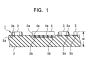
- Fig. 1 is a sectional view of an electronic circuit module according to an embodiment of the present invention
- Figs. 2A to 2D are sectional views showing a manufacturing process of the electronic circuit module
- Fig. 3 is a flowchart of the manufacturing process of the electronic circuit module.
- an electronic circuit module 1 includes a circuit board 2 which is composed of an alumina substrate or a ceramic substrate and which has a recess 2a in the top surface thereof and various kinds of chip components 3 and a flip chip IC 4 which are mounted on the circuit board 2.
- the chip components 3 and the flip chip IC 4 are reflow-soldered on lands 5 which are arranged on the top surface of the circuit board 2 and the bottom surface of the recess 2a.
- the circuit board 2 serves as a surface mount module which can be mounted on a motherboard (not shown) by reflow soldering, and is provided with a plurality of connecting terminals (not shown) which are to be reflow-soldered on connection lands arranged on the motherboard on the side and the bottom surfaces of the circuit board 2.
- the size of the recess 2a formed in the top surface of the circuit board 2 is slightly larger than the external size of the flip chip IC 4, and the depth thereof is about 0.2 mm to 0.3 mm.
- a plurality of lands 5 are arranged on the top surface of the circuit board 2 and the bottom surface of the recess 2a, and each land is electrically connected to a wiring pattern (not shown).
- the lands arranged on the top surface of the circuit board 2 are denoted by 5a and the lands arranged on the bottom surface of the recess 2a are denoted by 5b.
- Each of the chip components 3 may be a chip capacitor or a chip resistor, and external terminals 3a of the chip components 3 are reflow-soldered on the lands 5a on the top surface of the circuit board 2.
- the flip chip IC 4 is of a BGA type or a BCC type.
- the flip chip IC 4 is of the BGA type in which external connection lands are arranged on the bottom surface of the flip chip IC 4 in a grid pattern and solder balls 4a are adhered on the external connection lands.
- the solder balls 4a of the flip chip IC 4 are reflow-soldered on the lands 5b arranged on the bottom surface of the recess 2a.
- the circuit board 2 and a metal mask 6 are prepared.
- the circuit board 2 has the recess 2a in the top surface thereof, and the lands 5a and 5b are provided on the top surface of the circuit board 2 and the bottom surface of the recess 2a, respectively.
- the metal mask 6 has a projection 6a on the bottom surface thereof, and a plurality of through holes 6b are provided in the metal mask 6 in a region including the projection 6a.
- the projection 6a and the through holes 6b are formed by etching or laser processing, and the amount by which the projection 6a projects is set the same as the depth of the recess 2a formed in the circuit board 2 (0.2 mm to 0.3 mm).
- Step 2 of the flowchart shown in Fig. 3 solder cream 8 is applied to each of the lands 5a and 5b provided on the circuit board 2 using the metal mask 6.
- the metal mask 6 is placed on the circuit board 2 and is positioned with respect to the circuit board 2 such that the projection 6a is inserted into the recess 2a.
- the solder cream 8 is supplied into the through holes 6b in the metal mask 6 with a squeegee 7.
- the metal mask 6 is removed from the circuit board 2.
- the solder cream 8 is applied to each of the lands 5a and 5b provided on the circuit board 2.
- the solder cream 8 can be applied to the lands 5a and 5b provided on the top surface of the circuit board 2 and the bottom surface of the recess 2a, respectively, at the same time.
- Step 3 of the flowchart shown in Fig. 3 the chip components 3 and the flip chip IC 4 are mounted on the lands 5a and 5b, respectively, with the solder cream 8 provided therebetween.
- the chip components 3 are placed on the solder cream 8 applied to the lands 5a provided on the top surface of the circuit board 2 and the flip chip IC 4 is placed on the solder cream 8 applied to the lands 5b provided on the bottom surface of the recess 2a.
- Step 4 of the flowchart shown in Fig. 3 the chip components 3 and the flip chip IC 4 are reflow-soldered on the corresponding lands 5a and 5b, and thus the electronic circuit module 1 shown in Fig. 1 is completed. More specifically, the circuit board 2 on which the chip components 3 and the flip chip IC 4 are placed is put in a reflow oven (not shown), and the solder cream 8 is melted and solidified in the reflow oven so that the external terminals 3a of the chip components 3 are reflow-soldered on the lands 5a arranged on the top surface of the circuit board 2 and the solder balls 4a of the flip chip IC 4 are reflow-soldered on the lands 5b arranged on the bottom surface of the recess 2a, as shown in Fig. 1.
- the recess 2a is formed in the top surface of the circuit board 2 and the solder balls 4a of the flip chip IC 4 are reflow-soldered on the lands 5b arranged on the bottom surface of the recess 2a. Accordingly, the amount by which the flip chip IC 4 projects from the surface of the circuit board 2 can be reduced by the amount corresponding to the depth of the recess 2a. Therefore, although the flip chip IC 4, which has a greater height than the chip components 3, is mounted on the circuit board 2 along with the chip components 3, the thickness of the electronic circuit module 1 (indicated by W in Fig. 1) is relatively small.
- the metal mask 6 having the projection 6a on the back surface thereof is used and the solder cream 8 is applied while the projection 6a is in contact with the bottom surface of the recess 2a. Therefore, the solder cream 8 can be applied to the lands 5a provided on the top surface of the circuit board 2 and the lands 5b provided on the bottom surface of the recess 2a at the same time.
- solder cream 8 is applied to the lands 5a and 5b on the circuit board 2 at the same time using the metal mask 6 and the chip components 3 and the flip chip IC 4 are placed on the solder cream 8 and reflow-soldered on the lands 5a and 5b, respectively, all of the chip components 3 and the flip chip IC 4 can be mounted on the circuit board 2 in a single reflow-soldering process. Therefore, it is not necessary to use an expensive and complex mounting machine as in the case where an IC bare chip is attached by wire bonding or with stud bumps, and the inexpensive, low-profile electronic circuit module 1 can be manufactured at low cost.
- the flip chip IC 4 of the BGA type is described as an example of the surface-mount electronic component which is reflow-soldered in the recess 2a of the circuit board 2.
- a flip chip IC of the BCC type and a surface-mount electronic component other than the flip chip IC may also be used.
Landscapes
- Engineering & Computer Science (AREA)
- Microelectronics & Electronic Packaging (AREA)
- Manufacturing & Machinery (AREA)
- Electric Connection Of Electric Components To Printed Circuits (AREA)
- Structures For Mounting Electric Components On Printed Circuit Boards (AREA)
- Wire Bonding (AREA)
Abstract
A circuit board (2) having lands (5a,5b) provided on the top surface of the circuit board (2) and the bottom surface of a recess (2a) formed in the top surface and a metal mask (6) having a projection (6a) on the bottom surface thereof are prepared. The metal mask (6) is placed on the circuit board (2) such that the projection (6a) comes into contact with the bottom surface of the recess (2a), and solder cream (8) is applied to the lands (5a,5b) using the metal mask (6). Then, chip components (3) and a flip chip IC (4) are placed on the solder cream (8), and the circuit board (2) is put into a reflow oven where the solder cream (8) is melted and solidified so that external terminals of the chip components (3) are reflow-soldered on the lands (5a) on the top surface of the circuit board (2) and solder balls (4a) of the flip chip IC (4) are reflow-soldered on the lands (5b) on the bottom surface of the recess (2a).
Description
- The present invention relates to electronic circuit modules in which various surface-mount electronic components are soldered on a circuit board and methods for manufacturing the electronic circuit modules. More specifically, the present invention relates to an electronic circuit module in which the surface-mount electronic components include chip components, such as a chip resistor and a chip capacitor, and a flip chip IC of a ball grid array (BGA) type or a bump chip carrier (BCC) type and a method for manufacturing the electronic circuit module.
- Recently, the size of electronic devices has been reduced and electronic circuit modules in which surface-mount electronic components, such as chip components and semiconductor integrated circuit (IC) components, are mounted on a circuit board at high density have been developed.
- As a first example of such an electronic circuit module, Japanese Unexamined Patent Application Publication No. 7-211854 discloses, in
page 2 and Fig. 6, a module in which chip components and a flip chip IC are reflow-soldered on a plurality of lands arranged on the surface of a circuit board. When the electronic circuit module is manufactured, solder cream is applied to each of the lands on the circuit board using a metal mask, and the chip components and the flip chip IC are placed on the solder cream. Then, the circuit board is put in a reflow oven so that the chip components and the flip chip IC are reflow-soldered on the corresponding lands. - In addition, as a second example, an electronic circuit module in which the circuit components mounted on the circuit board include chip components which are reflow-soldered on lands and an IC bare chip which is adhered to the circuit board and is connected to the lands by wire bonding or with stud bumps is also known in the art.
- In the electronic circuit module according to the first example in which the chip components and the flip chip IC are reflow-soldered, the thickness of the electronic circuit module is determined by the height of the flip chip IC which projects from the surface of the circuit board since the flip chip IC is larger than the chip components. Therefore, there is a limit to reducing the thickness of the electronic circuit module for this reason.
- In comparison, the thickness of the electronic circuit module according to the second example in which the IC bare chip is mounted on the circuit board can be reduced since the height of the bare chip is sufficiently small relative to that of the flip chip IC. However, since the bare chip cannot be reflow-soldered like the chip components, it must be connected to the lands by wire bonding or with stud bumps. Accordingly, the manufacturing process is complex and an expensive mounting machine is required. Thus, there is a problem in that the total cost of the electronic circuit module increases.
- In view of the above-described situation, an object of the present invention is to provide an inexpensive, low-profile electronic circuit module.
- In order to attain this object, an electronic circuit module according to the present invention includes a circuit board having a recess in a surface of the circuit board; lands which are arranged on the surface of the circuit board and the bottom surface of the recess; and surface-mount electronic components which are reflow-soldered on the lands.
- In the electronic circuit module which is constructed as described above, even when one of the surface-mount electronic components which is mounted on the bottom surface of the recess has a greater height than the other surface-mount electronic components, the amount by which the surface-mount electronic component mounted on the bottom surface of the recess projects from the surface of the circuit board is reduced by the amount corresponding to the depth of the recess. Therefore, the thickness of the electronic circuit module can be reduced. In addition, since the surface-mount electronic components are reflow-soldered on the lands arranged on the surface of the circuit board and the bottom surface of the recess, all of the surface-mount electronic components can be attached to the circuit board in a single reflow-soldering process. Therefore, the manufacturing cost can be reduced and an inexpensive electronic circuit module can be obtained. In the electronic circuit module, preferably, the surface-mount electronic component mounted on the bottom surface of the recess is a flip chip IC and the other surface-mount electronic components which are mounted on the surface of the circuit board are chip components.
- In addition, in order to attain the above-described object, a method for manufacturing an electronic circuit module according to the present invention includes the steps of forming a recess in a surface of a circuit board; providing lands on the surface of the circuit board and the bottom surface of the recess; placing a metal mask on the surface of the circuit board, the metal mask having a flat top surface and a bottom surface provided with a projection, and positioning the projection with respect to the recess; applying solder cream to each of the lands through the metal mask; placing surface-mount electronic components on the lands with the solder cream interposed between each of the surface-mount electronic components and the corresponding lands; and putting the circuit board in a reflow oven and reflow-soldering the surface-mount electronic components to the corresponding lands.
- In the electronic circuit module which is manufactured by the above-described method, the solder cream is applied to each of the lands arranged on the surface of the circuit board and the bottom surface of the recess using a metal mask having a projection. Then, the surface-mount electronic components are placed on the solder cream and are reflow-soldered on the corresponding lands. Accordingly, all of the surface-mount electronic components can be attached to the circuit board in a single reflow-soldering process. Therefore, the manufacturing cost can be reduced and an inexpensive electronic circuit module can be obtained. In addition, even when one of the surface-mount electronic components which is mounted on the bottom surface of the recess has a greater height than the other surface-mount electronic components, the amount by which the surface-mount electronic component mounted on the bottom surface of the recess projects from the surface of the circuit board is reduced by the amount corresponding to the depth of the recess. Therefore, the thickness of the electronic circuit module can be reduced.
-
- Fig. 1 is a sectional view of an electronic circuit module according to an embodiment of the present invention;
- Figs. 2A to 2D are sectional views showing a manufacturing process of the electronic circuit module; and
- Fig. 3 is a flowchart of the manufacturing process of the electronic circuit module.
- An embodiment of the present invention will be described below with reference to the accompanying drawings. Fig. 1 is a sectional view of an electronic circuit module according to an embodiment of the present invention, Figs. 2A to 2D are sectional views showing a manufacturing process of the electronic circuit module, and Fig. 3 is a flowchart of the manufacturing process of the electronic circuit module.
- As shown in Fig. 1, an
electronic circuit module 1 according to the present embodiment includes acircuit board 2 which is composed of an alumina substrate or a ceramic substrate and which has arecess 2a in the top surface thereof and various kinds ofchip components 3 and aflip chip IC 4 which are mounted on thecircuit board 2. Thechip components 3 and theflip chip IC 4 are reflow-soldered on lands 5 which are arranged on the top surface of thecircuit board 2 and the bottom surface of therecess 2a. - The
circuit board 2 serves as a surface mount module which can be mounted on a motherboard (not shown) by reflow soldering, and is provided with a plurality of connecting terminals (not shown) which are to be reflow-soldered on connection lands arranged on the motherboard on the side and the bottom surfaces of thecircuit board 2. The size of therecess 2a formed in the top surface of thecircuit board 2 is slightly larger than the external size of theflip chip IC 4, and the depth thereof is about 0.2 mm to 0.3 mm. A plurality of lands 5 are arranged on the top surface of thecircuit board 2 and the bottom surface of therecess 2a, and each land is electrically connected to a wiring pattern (not shown). For illustration, the lands arranged on the top surface of thecircuit board 2 are denoted by 5a and the lands arranged on the bottom surface of therecess 2a are denoted by 5b. - Each of the
chip components 3 may be a chip capacitor or a chip resistor, andexternal terminals 3a of thechip components 3 are reflow-soldered on thelands 5a on the top surface of thecircuit board 2. Theflip chip IC 4 is of a BGA type or a BCC type. In the present embodiment, theflip chip IC 4 is of the BGA type in which external connection lands are arranged on the bottom surface of theflip chip IC 4 in a grid pattern andsolder balls 4a are adhered on the external connection lands. Thesolder balls 4a of theflip chip IC 4 are reflow-soldered on thelands 5b arranged on the bottom surface of therecess 2a. - Next, a method for manufacturing the
electronic circuit module 1 having the above-described construction will be described below with reference to Figs. 2A to 2D and 3. - First, in
Step 1 of the flowchart shown in Fig. 3, thecircuit board 2 and a metal mask 6 are prepared. As described above, thecircuit board 2 has therecess 2a in the top surface thereof, and thelands circuit board 2 and the bottom surface of therecess 2a, respectively. In addition, as shown in Fig. 2A, the metal mask 6 has aprojection 6a on the bottom surface thereof, and a plurality of throughholes 6b are provided in the metal mask 6 in a region including theprojection 6a. Theprojection 6a and the throughholes 6b are formed by etching or laser processing, and the amount by which theprojection 6a projects is set the same as the depth of therecess 2a formed in the circuit board 2 (0.2 mm to 0.3 mm). - Next, in
Step 2 of the flowchart shown in Fig. 3,solder cream 8 is applied to each of thelands circuit board 2 using the metal mask 6. In this step, first, the metal mask 6 is placed on thecircuit board 2 and is positioned with respect to thecircuit board 2 such that theprojection 6a is inserted into therecess 2a. Then, as shown in Fig. 2B, thesolder cream 8 is supplied into the throughholes 6b in the metal mask 6 with asqueegee 7. Then, the metal mask 6 is removed from thecircuit board 2. Accordingly, as shown in Fig. 2C, thesolder cream 8 is applied to each of thelands circuit board 2. Since the metal mask 6 has theprojection 6a which comes into contact with the bottom surface of therecess 2a, thesolder cream 8 can be applied to thelands circuit board 2 and the bottom surface of therecess 2a, respectively, at the same time. - Next, in
Step 3 of the flowchart shown in Fig. 3, thechip components 3 and theflip chip IC 4 are mounted on thelands solder cream 8 provided therebetween. In this step, as shown in Fig. 2D, thechip components 3 are placed on thesolder cream 8 applied to thelands 5a provided on the top surface of thecircuit board 2 and theflip chip IC 4 is placed on thesolder cream 8 applied to thelands 5b provided on the bottom surface of therecess 2a. - Next, in
Step 4 of the flowchart shown in Fig. 3, thechip components 3 and theflip chip IC 4 are reflow-soldered on thecorresponding lands electronic circuit module 1 shown in Fig. 1 is completed. More specifically, thecircuit board 2 on which thechip components 3 and theflip chip IC 4 are placed is put in a reflow oven (not shown), and thesolder cream 8 is melted and solidified in the reflow oven so that theexternal terminals 3a of thechip components 3 are reflow-soldered on thelands 5a arranged on the top surface of thecircuit board 2 and thesolder balls 4a of theflip chip IC 4 are reflow-soldered on thelands 5b arranged on the bottom surface of therecess 2a, as shown in Fig. 1. - As described above, in the
electronic circuit module 1 according to the present embodiment, therecess 2a is formed in the top surface of thecircuit board 2 and thesolder balls 4a of theflip chip IC 4 are reflow-soldered on thelands 5b arranged on the bottom surface of therecess 2a. Accordingly, the amount by which theflip chip IC 4 projects from the surface of thecircuit board 2 can be reduced by the amount corresponding to the depth of therecess 2a. Therefore, although theflip chip IC 4, which has a greater height than thechip components 3, is mounted on thecircuit board 2 along with thechip components 3, the thickness of the electronic circuit module 1 (indicated by W in Fig. 1) is relatively small. In addition, when theelectronic circuit module 1 is manufactured, the metal mask 6 having theprojection 6a on the back surface thereof is used and thesolder cream 8 is applied while theprojection 6a is in contact with the bottom surface of therecess 2a. Therefore, thesolder cream 8 can be applied to thelands 5a provided on the top surface of thecircuit board 2 and thelands 5b provided on the bottom surface of therecess 2a at the same time. Since thesolder cream 8 is applied to thelands circuit board 2 at the same time using the metal mask 6 and thechip components 3 and theflip chip IC 4 are placed on thesolder cream 8 and reflow-soldered on thelands chip components 3 and theflip chip IC 4 can be mounted on thecircuit board 2 in a single reflow-soldering process. Therefore, it is not necessary to use an expensive and complex mounting machine as in the case where an IC bare chip is attached by wire bonding or with stud bumps, and the inexpensive, low-profileelectronic circuit module 1 can be manufactured at low cost. - In the above-described embodiment, the
flip chip IC 4 of the BGA type is described as an example of the surface-mount electronic component which is reflow-soldered in therecess 2a of thecircuit board 2. However, a flip chip IC of the BCC type and a surface-mount electronic component other than the flip chip IC may also be used.
Claims (3)
- An electronic circuit module comprising:a circuit board having a recess in a surface of the circuit board;lands which are arranged on the surface of the circuit board and the bottom surface of the recess; andsurface-mount electronic components which are reflow-soldered on the lands.
- An electronic circuit module according to Claim 1, wherein the surface-mount electronic components include chip components which are soldered on the surface of the circuit board and a flip chip IC which is soldered on the bottom surface of the recess.
- A method for manufacturing an electronic circuit module comprising the steps of:forming a recess in a surface of a circuit board;providing lands on the surface of the circuit board and the bottom surface of the recess;placing a metal mask on the surface of the circuit board, the metal mask having a flat top surface and a bottom surface provided with a projection, and positioning the projection with respect to the recess;applying solder cream to each of the lands through the metal mask;placing surface-mount electronic components on the lands with the solder cream interposed between each of the surface-mount electronic components and the corresponding lands; andputting the circuit board in a reflow oven and reflow-soldering the surface-mount electronic components to the corresponding lands.
Applications Claiming Priority (2)
| Application Number | Priority Date | Filing Date | Title |
|---|---|---|---|
| JP2003078121A JP2004288820A (en) | 2003-03-20 | 2003-03-20 | Electronic circuit module and method of manufacturing the same |
| JP2003078121 | 2003-03-20 |
Publications (1)
| Publication Number | Publication Date |
|---|---|
| EP1460888A1 true EP1460888A1 (en) | 2004-09-22 |
Family
ID=32821388
Family Applications (1)
| Application Number | Title | Priority Date | Filing Date |
|---|---|---|---|
| EP04006246A Withdrawn EP1460888A1 (en) | 2003-03-20 | 2004-03-16 | Low-profile electronic circuit module and method for manufacturing the same |
Country Status (3)
| Country | Link |
|---|---|
| US (1) | US20040183186A1 (en) |
| EP (1) | EP1460888A1 (en) |
| JP (1) | JP2004288820A (en) |
Cited By (4)
| Publication number | Priority date | Publication date | Assignee | Title |
|---|---|---|---|---|
| EP2408282A1 (en) * | 2010-07-12 | 2012-01-18 | Sony Ericsson Mobile Communications AB | Module connection in a printed wiring board |
| CN103192150A (en) * | 2013-03-29 | 2013-07-10 | 上海安费诺永亿通讯电子有限公司 | Electronic component welding method |
| DE102013114044A1 (en) * | 2013-12-13 | 2015-06-18 | Endress + Hauser Gmbh + Co. Kg | Printing template for printing printed circuit boards |
| CN114080104A (en) * | 2020-08-19 | 2022-02-22 | 荣耀终端有限公司 | Circuit board assembly and electronic equipment |
Families Citing this family (10)
| Publication number | Priority date | Publication date | Assignee | Title |
|---|---|---|---|---|
| JP2009104888A (en) * | 2007-10-23 | 2009-05-14 | Nec Tokin Corp | Protection module |
| US8955735B2 (en) * | 2013-05-17 | 2015-02-17 | Zen Voce Corporation | Method for enhancing the yield rate of ball implanting of a substrate of an integrated circuit |
| US9120170B2 (en) * | 2013-11-01 | 2015-09-01 | Zen Voce Corporation | Apparatus and method for placing and mounting solder balls on an integrated circuit substrate |
| DE102013020189B4 (en) * | 2013-12-02 | 2015-11-05 | Cadilac Laser Gmbh Cad Industrial Lasercutting | Printing template and method for its production |
| WO2018063150A1 (en) * | 2016-09-27 | 2018-04-05 | Intel Corporation | Frame embedded components |
| US11444400B2 (en) * | 2020-12-21 | 2022-09-13 | Dell Products L.P. | Information handling system with a printed circuit board having an embedded interconnect |
| US20220110214A1 (en) * | 2021-12-14 | 2022-04-07 | Intel Corporation | Stepped package and recessed circuit board |
| CN118947231A (en) * | 2022-05-17 | 2024-11-12 | 歌尔股份有限公司 | Circuit board, electronic device and method for manufacturing the circuit board |
| US20250006689A1 (en) * | 2023-06-30 | 2025-01-02 | Adeia Semiconductor Bonding Technologies Inc. | Structures and methods for bonding dies |
| CN119028848B (en) * | 2024-08-19 | 2025-09-19 | 江西万年芯微电子有限公司 | Processing method for synchronously sintering passive device and chip and semiconductor assembly |
Citations (3)
| Publication number | Priority date | Publication date | Assignee | Title |
|---|---|---|---|---|
| JPH01101689A (en) * | 1987-10-15 | 1989-04-19 | Matsushita Electric Works Ltd | Printed wiring board for mounting electronic component |
| EP0774888A2 (en) * | 1995-11-16 | 1997-05-21 | Matsushita Electric Industrial Co., Ltd | Printing wiring board and assembly of the same |
| EP0915641A1 (en) * | 1997-11-05 | 1999-05-12 | Nec Corporation | Surface mount assembly for electronic components |
-
2003
- 2003-03-20 JP JP2003078121A patent/JP2004288820A/en not_active Withdrawn
-
2004
- 2004-03-16 EP EP04006246A patent/EP1460888A1/en not_active Withdrawn
- 2004-03-16 US US10/801,317 patent/US20040183186A1/en not_active Abandoned
Patent Citations (3)
| Publication number | Priority date | Publication date | Assignee | Title |
|---|---|---|---|---|
| JPH01101689A (en) * | 1987-10-15 | 1989-04-19 | Matsushita Electric Works Ltd | Printed wiring board for mounting electronic component |
| EP0774888A2 (en) * | 1995-11-16 | 1997-05-21 | Matsushita Electric Industrial Co., Ltd | Printing wiring board and assembly of the same |
| EP0915641A1 (en) * | 1997-11-05 | 1999-05-12 | Nec Corporation | Surface mount assembly for electronic components |
Non-Patent Citations (1)
| Title |
|---|
| PATENT ABSTRACTS OF JAPAN vol. 013, no. 343 (E - 796) 2 August 1989 (1989-08-02) * |
Cited By (5)
| Publication number | Priority date | Publication date | Assignee | Title |
|---|---|---|---|---|
| EP2408282A1 (en) * | 2010-07-12 | 2012-01-18 | Sony Ericsson Mobile Communications AB | Module connection in a printed wiring board |
| CN103192150A (en) * | 2013-03-29 | 2013-07-10 | 上海安费诺永亿通讯电子有限公司 | Electronic component welding method |
| DE102013114044A1 (en) * | 2013-12-13 | 2015-06-18 | Endress + Hauser Gmbh + Co. Kg | Printing template for printing printed circuit boards |
| CN114080104A (en) * | 2020-08-19 | 2022-02-22 | 荣耀终端有限公司 | Circuit board assembly and electronic equipment |
| CN114080104B (en) * | 2020-08-19 | 2022-09-27 | 荣耀终端有限公司 | Circuit board assembly and electronic equipment |
Also Published As
| Publication number | Publication date |
|---|---|
| US20040183186A1 (en) | 2004-09-23 |
| JP2004288820A (en) | 2004-10-14 |
Similar Documents
| Publication | Publication Date | Title |
|---|---|---|
| US6493240B2 (en) | Interposer for connecting two substrates and resulting assembly | |
| US5367435A (en) | Electronic package structure and method of making same | |
| US5926731A (en) | Method for controlling solder bump shape and stand-off height | |
| KR100649036B1 (en) | Method of production of semiconductor device | |
| JPH04256343A (en) | Flip-chip package for integrated circuit use | |
| US5770477A (en) | Flip chip-on-flip chip multi-chip module | |
| US20040183186A1 (en) | Low-profile electronic circuit module and method for manufacturing the same | |
| JP3063709B2 (en) | Electronic component mounting structure, mounting substrate and electronic component mounting method | |
| JPH08111578A (en) | Method for manufacturing substrate for mounting ball grid array package | |
| JPH05259372A (en) | Hibrid ic | |
| US20050078457A1 (en) | Small memory card | |
| JP2002368027A (en) | Method for manufacturing semiconductor device | |
| JPH10313170A (en) | Wiring board | |
| JP3855874B2 (en) | Electronic component mounting method, IC chip mounting method, and IC chip | |
| JPH11112121A (en) | Circuit module and electronic equipment incorporating circuit module | |
| JP2001085558A (en) | Semiconductor device and mounting method thereof | |
| JP2006253167A (en) | Method of manufacturing cavity structure printed wiring board and mounting structure | |
| JPH11345831A (en) | Semiconductor device, mounting substrate, and mounting method | |
| JPH01138791A (en) | Hybrid integrated circuit device | |
| JP2004327912A (en) | Semiconductor package and semiconductor device | |
| JP2553989Y2 (en) | Electronic components | |
| JPH08274425A (en) | Printed wiring board | |
| JPH04243187A (en) | Printed circuit board | |
| US20070200252A1 (en) | Circuit board apparatus, circuit component reinforcing method and electronic device | |
| JP2641405B2 (en) | Electronic component mounting apparatus and mounting method |
Legal Events
| Date | Code | Title | Description |
|---|---|---|---|
| PUAI | Public reference made under article 153(3) epc to a published international application that has entered the european phase |
Free format text: ORIGINAL CODE: 0009012 |
|
| AK | Designated contracting states |
Kind code of ref document: A1 Designated state(s): AT BE BG CH CY CZ DE DK EE ES FI FR GB GR HU IE IT LI LU MC NL PL PT RO SE SI SK TR |
|
| AX | Request for extension of the european patent |
Extension state: AL LT LV MK |
|
| AKX | Designation fees paid | ||
| REG | Reference to a national code |
Ref country code: DE Ref legal event code: 8566 |
|
| STAA | Information on the status of an ep patent application or granted ep patent |
Free format text: STATUS: THE APPLICATION IS DEEMED TO BE WITHDRAWN |
|
| 18D | Application deemed to be withdrawn |
Effective date: 20050323 |