EP1460678A1 - Method and apparatus for cleaning and method and apparatus for etching - Google Patents
Method and apparatus for cleaning and method and apparatus for etching Download PDFInfo
- Publication number
- EP1460678A1 EP1460678A1 EP01954400A EP01954400A EP1460678A1 EP 1460678 A1 EP1460678 A1 EP 1460678A1 EP 01954400 A EP01954400 A EP 01954400A EP 01954400 A EP01954400 A EP 01954400A EP 1460678 A1 EP1460678 A1 EP 1460678A1
- Authority
- EP
- European Patent Office
- Prior art keywords
- gas
- aforesaid
- fluorine
- product
- mixed
- Prior art date
- Legal status (The legal status is an assumption and is not a legal conclusion. Google has not performed a legal analysis and makes no representation as to the accuracy of the status listed.)
- Withdrawn
Links
Images


Classifications
-
- B—PERFORMING OPERATIONS; TRANSPORTING
- B08—CLEANING
- B08B—CLEANING IN GENERAL; PREVENTION OF FOULING IN GENERAL
- B08B7/00—Cleaning by methods not provided for in a single other subclass or a single group in this subclass
- B08B7/0035—Cleaning by methods not provided for in a single other subclass or a single group in this subclass by radiant energy, e.g. UV, laser, light beam or the like
-
- C—CHEMISTRY; METALLURGY
- C23—COATING METALLIC MATERIAL; COATING MATERIAL WITH METALLIC MATERIAL; CHEMICAL SURFACE TREATMENT; DIFFUSION TREATMENT OF METALLIC MATERIAL; COATING BY VACUUM EVAPORATION, BY SPUTTERING, BY ION IMPLANTATION OR BY CHEMICAL VAPOUR DEPOSITION, IN GENERAL; INHIBITING CORROSION OF METALLIC MATERIAL OR INCRUSTATION IN GENERAL
- C23C—COATING METALLIC MATERIAL; COATING MATERIAL WITH METALLIC MATERIAL; SURFACE TREATMENT OF METALLIC MATERIAL BY DIFFUSION INTO THE SURFACE, BY CHEMICAL CONVERSION OR SUBSTITUTION; COATING BY VACUUM EVAPORATION, BY SPUTTERING, BY ION IMPLANTATION OR BY CHEMICAL VAPOUR DEPOSITION, IN GENERAL
- C23C16/00—Chemical coating by decomposition of gaseous compounds, without leaving reaction products of surface material in the coating, i.e. chemical vapour deposition [CVD] processes
- C23C16/44—Chemical coating by decomposition of gaseous compounds, without leaving reaction products of surface material in the coating, i.e. chemical vapour deposition [CVD] processes characterised by the method of coating
- C23C16/4401—Means for minimising impurities, e.g. dust, moisture or residual gas, in the reaction chamber
- C23C16/4405—Cleaning of reactor or parts inside the reactor by using reactive gases
-
- C—CHEMISTRY; METALLURGY
- C23—COATING METALLIC MATERIAL; COATING MATERIAL WITH METALLIC MATERIAL; CHEMICAL SURFACE TREATMENT; DIFFUSION TREATMENT OF METALLIC MATERIAL; COATING BY VACUUM EVAPORATION, BY SPUTTERING, BY ION IMPLANTATION OR BY CHEMICAL VAPOUR DEPOSITION, IN GENERAL; INHIBITING CORROSION OF METALLIC MATERIAL OR INCRUSTATION IN GENERAL
- C23C—COATING METALLIC MATERIAL; COATING MATERIAL WITH METALLIC MATERIAL; SURFACE TREATMENT OF METALLIC MATERIAL BY DIFFUSION INTO THE SURFACE, BY CHEMICAL CONVERSION OR SUBSTITUTION; COATING BY VACUUM EVAPORATION, BY SPUTTERING, BY ION IMPLANTATION OR BY CHEMICAL VAPOUR DEPOSITION, IN GENERAL
- C23C16/00—Chemical coating by decomposition of gaseous compounds, without leaving reaction products of surface material in the coating, i.e. chemical vapour deposition [CVD] processes
- C23C16/44—Chemical coating by decomposition of gaseous compounds, without leaving reaction products of surface material in the coating, i.e. chemical vapour deposition [CVD] processes characterised by the method of coating
- C23C16/448—Chemical coating by decomposition of gaseous compounds, without leaving reaction products of surface material in the coating, i.e. chemical vapour deposition [CVD] processes characterised by the method of coating characterised by the method used for generating reactive gas streams, e.g. by evaporation or sublimation of precursor materials
- C23C16/4488—Chemical coating by decomposition of gaseous compounds, without leaving reaction products of surface material in the coating, i.e. chemical vapour deposition [CVD] processes characterised by the method of coating characterised by the method used for generating reactive gas streams, e.g. by evaporation or sublimation of precursor materials by in situ generation of reactive gas by chemical or electrochemical reaction
-
- H—ELECTRICITY
- H10—SEMICONDUCTOR DEVICES; ELECTRIC SOLID-STATE DEVICES NOT OTHERWISE PROVIDED FOR
- H10P—GENERIC PROCESSES OR APPARATUS FOR THE MANUFACTURE OR TREATMENT OF DEVICES COVERED BY CLASS H10
- H10P72/00—Handling or holding of wafers, substrates or devices during manufacture or treatment thereof
- H10P72/04—Apparatus for manufacture or treatment
- H10P72/0402—Apparatus for fluid treatment
- H10P72/0418—Apparatus for fluid treatment for etching
Definitions
- CIF 3 gas is filled as a high-purity liquefied gas into metal cylinders and is delivered in this form to the user's site.
- the gas-phase portion of the CIF 3 is withdrawn from the cylinder, is depressurized to the vapor pressure prevailing at the cylinder temperature at this point (or to below this vapor pressure), and is then transported to the particular semiconductor fabrication apparatus.
- CIF 3 Since CIF 3 has a low boiling point at 12°C, a precise temperature control must be exercised - in particular when large CIF 3 gas flow rates are required - over the associated pumps and supply conduit system in order to obtain the required quantities of the gas and in order to prevent reliquefaction along the conduit pathways.
- CIF 3 is very corrosive and strongly oxidizing and in particular has a very high reactivity in its liquid phase. This places limitations from a materials standpoint on the ability to heat the pumps and conduits, while at the same time heating the pumps and conduits is also undesirable from a practical standpoint.
- the storage and transport of this highly reactive liquefied CIF 3 gas is tightly regulated in the United States and Europe, which places limitations on its range of applications notwithstanding the fact that it is a highly desirable cleaning gas.
- the object of this invention is to provide improvements in the safety, cost, and flexibility of the IFCG-based cleaning methods and apparatuses and IFCG-based etching methods and apparatuses that are used in semiconductor processing systems.
- This invention which achieves the aforesaid object, is essentially characterized by the onsite and on-demand production and supply of IFCG.
- onsite means that the IFCG-producing mechanism is combined with the main processing mechanism of the semiconductor processing system.
- On-demand is taken to mean that the process gas can be supplied in accordance with the timing required by the main processing mechanism and in accordance with any component adjustment required by the main processing mechanism.
- the first halogen gas : fluorine gas : inert gas volumetric ratio in the mixed gas in the method of the first aspect is established at 10 - 90: 10 - 90 : 0 - 90.
- the aforesaid inert gas in the method of the first, second, or third aspect is helium.
- a fifth aspect of this invention comprises a cleaning apparatus that removes by-product containing material selected from the group consisting of Si, Mo, Ta, W, SiO x , SiN x , SiON, SiC, SiGe, TaSi x , TaO x , WSi x , TiC, TiN, TiW, BN, and ITO, that has accumulated in the treating chamber of a semiconductor processing system, wherein said cleaning apparatus is provided with an upstream section that forms a mixed gas by mixing the gases afforded by the independent introduction of a nonfluorine first halogen gas and fluorine gas from, respectively, a first gas source and a second gas source, and the selective introduction of inert gas from a third gas source, and a downstream section that produces a product gas containing IFCG by feeding the aforesaid mixed gas into a heated reactor and heating said mixed gas to a temperature at which the first halogen gas and fluorine gas react, and that feeds said product gas concurrent with its production into
- the upstream section in the apparatus of the fifth aspect is provided with a controller that can vary the first halogen gas : fluorine gas : inert gas volumetric ratio in the aforesaid mixed gas through independent adjustment of the individual flow rates of the first halogen gas, fluorine gas, and inert gas.
- An eighth aspect of this invention comprises a method for etching in a semiconductor processing system, that etches a first film on a treatment substrate, said first film substantially comprising material selected from the group consisting of Si, SIPOS (semi-insulating polycrystalline silicon), Ta, and TaSi x , wherein said etching method is provided with a process comprising the formation of a mixed gas by mixing the gases afforded by independently introducing a nonfluorine first halogen gas and fluorine gas from, respectively, a first gas source and a second gas source, and selectively introducing inert gas from a third gas source, and a process in which a product gas containing IFCG is produced by feeding the aforesaid mixed gas into a heated reactor and heating said mixed gas to a temperature at which the first halogen gas and fluorine gas react, and in which said product gas is fed concurrent with its production into the aforesaid treating chamber.
- a second film is present in the method of the eighth aspect on the aforesaid treatment substrate, wherein said second film substantially comprises material selected from the group consisting of SiO 2 , SiN x , SiON, TaO x , and photoresists and the aforesaid etching method etches the aforesaid first film selectively relative to the said second film.
- a tenth aspect of this invention is an etching apparatus in a semiconductor processing system, that etches a first film on a treatment substrate, said first film substantially comprising material selected from the group consisting of Si, SIPOS, Ta, and TaSi x , wherein said etching apparatus is provided with a treating chamber that holds the aforesaid treatment substrate, an upstream section that forms a mixed gas by mixing the gases afforded by the independent introduction of a nonfluorine first halogen gas and fluorine gas from, respectively, a first gas source and a second gas source, and the selective introduction of inert gas from a third gas source, and a downstream section that produces a product gas containing IFCG by feeding the aforesaid mixed gas into a heated reactor and heating said mixed gas to a temperature at which the first halogen gas and fluorine gas react, and that feeds said product gas concurrent with its production into the aforesaid treating chamber.
- FIG. 1 contains a schematic drawing of a cleaning apparatus that is an embodiment of this invention and that removes by-product that has accumulated within the treating chamber of a semiconductor processing system.
- This cleaning apparatus 30 may be connected to, for example, a CVD apparatus 10 set up to form a silicon film on a treatment substrate, e.g., a semiconductor wafer or LCD substrate.
- the cleaning apparatus 30 in accordance with this invention is used to remove this by-product.
- the cleaning apparatus 30 is provided with a first gas source 32 , a second gas source 34 , and a third gas source 36 in order to supply, respectively, chlorine (Cl 2 ) gas, fluorine (F 2 ) gas, and inert gas.
- the chlorine gas source 32 comprises a cylinder filled with the liquefied gas. Feed of the chlorine gas is relatively easy due to the high vapor pressure involved.
- the fluorine second gas source 34 comprises a gas generator that produces fluorine gas by electrolysis, although the fluorine gas could also be supplied as a high-pressure gas from a cylinder.
- the chlorine gas from the first gas source 32 , the fluorine gas from the second gas source 34 , and the inert gas from the third gas source 36 pass through, respectively, mass flow controller (MFC) 38a , MFC 38b , and MFC 38c , which results in their introduction with their flow rates under separate and independent control.
- MFC mass flow controller
- the independently introduced chlorine gas, fluorine gas, and inert gas are combined and mixed in the conduit 42 to form a mixed gas.
- the chlorine gas : fluorine gas : inert gas volumetric ratio established in this mixed gas should be 10 - 90 : 10 - 90 : 0 - 90.
- the product gas withdrawn from the cooler 46 is first passed through an analyzer 48 that measures the interhalogen fluorine compound.
- the measurement results afforded by the analyzer 48 are fedback to the main controller 52 , and the MFCs 38a, 38b, and 38c are adjusted on the basis of these measurement results. This effects adjustment in such a manner that the chlorine gas : fluorine gas : inert gas volumetric ratio in the mixed gas is brought to the prescribed value.
- the flow rate and pressure of the product gas are then adjusted in the buffer 54 so as to compatibilize these parameters with the conditions in the treating chamber 12 of the CVD apparatus 10 . After this adjustment the product gas is fed to the treating chamber 12 .
- the buffer 54 can also be executed as a temporary storage section that carries out liquefaction of the product gas and its ensuing re-volatilization. This enables the removal of solids and unreacted volatile gases, gaseous by-products, and impurity gases from the product gas in the buffer 54 .
- the chlorine fluoride gas (e.g., CIF 3 gas) in the product gas fed into the treating chamber 12 reacts with the by-product (main component Si) that has accumulated on the inner walls of the treating chamber 12 and the inner walls of the exhaust system 16 and thereby debonds same from these inner walls.
- the debonded by-product becomes entrained in the exhaust flow produced by the action of the exhaust system 16 and is flushed from the CVD apparatus 10 .
- chlorine fluoride gas is also effective for the removal of substances other than silicon (silicon includes polysilicon and amorphous silicon).
- silicon includes polysilicon and amorphous silicon.
- These substances other than silicon can be specifically exemplified by Mo, Ta, W, SiO x , SiN x , SiON, SiC, SiGe, TaSi x , TaO x , WSi x , TiC, TiN, TiW, BN, and ITO.
- the cleaning apparatus 30 can be effectively used for the cleaning, inter alia, of CVD equipment and etching equipment in which by-product containing material selected from the aforesaid material group has been produced by the particular primary process implemented in the equipment.
- a mixed gas of 30 SCCM chlorine gas, 100 SCCM fluorine gas, and 100 SCCM helium was produced and continuously fed at an internal system pressure of 836 torr into a heated reactor 44 comprising a nickel heat exchanger heated to 250°C to 350°C.
- a product gas was obtained that in the vicinity of the outlet from the heated reactor 44 had a CIF 3 concentration of 10% to 30%, giving a CIF 3 yield of 60% to 80%.
- FIG. 2 contains a schematic drawing of an etching apparatus that is another embodiment of this invention, said etching apparatus residing in a semiconductor processing system.
- This etching apparatus 60 can be used, for example, to etch an Si film on a treatment substrate in preference to an SiO 2 film (selective etching).
- the treatment substrate can be, for example, a semiconductor wafer or LCD substrate.
- the etching apparatus 60 is provided with a treating chamber 62 that holds the treatment substrate. Disposed within the treating chamber 62 is a platform 64 for mounting the treatment substrate. The lower region of the treating chamber 62 is connected to an exhaust system 66 that exhausts the interior and establishes a vacuum therein. The upper region of the treating chamber 62 is connected to a feed system 70 that supplies etching gas.
- the feed system 70 in the etching apparatus 60 has the same structure as the cleaning apparatus 30 that is illustrated in Figure 1.
- this feed system 70 is provided with a first gas source 72 , a second gas source 74 , and a third gas source 76 in order to supply, respectively, chlorine (Cl 2 ) gas, fluorine (F 2 ) gas, and inert gas.
- the chlorine gas from the first gas source 72 , the fluorine gas from the second gas source 74 , and the inert gas from the third gas source 76 pass through, respectively, MFC 78a , MFC 78b , and MFC 78c , which results in their introduction with their flow rates under separate and independent control.
- the independently introduced chlorine gas, fluorine gas, and inert gas are combined and mixed in the conduit 82 to form a mixed gas.
- the chlorine gas : fluorine gas : inert gas volumetric ratio established in this mixed gas should be 10 - 90 : 10 - 90 : 0 - 90.
- the mixed gas generated in this manner is transported into a heated reactor 84 , for example, a heat exchanger, and is heated to 200°C to 400°C and preferably 250°C to 350°C.
- This serves to produce a product gas containing chlorine fluoride gas, e.g., CIF 3 gas, through reaction of the chlorine gas and fluorine gas.
- This product gas which will contain CIF 3 gas as its main component along with other chlorine fluoride gases (CIF, CIF 5 , etc.), by-products, and unreacted gases, is cooled by the cooler 86 to around room temperature - where CIF 3 does not liquefy - and is discharged at a pressure at which the CIF 3 does not liquefy.
- the product gas withdrawn from the cooler 86 is first passed through an analyzer 88 that measures the interhalogen fluorine compound.
- the measurement results afforded by the analyzer 88 are fedback to the main controller 92 , and the MFCs 78a , 78b , and 78c are adjusted on the basis of these measurement results. This effects adjustment in such a manner that the chlorine gas : fluorine gas : inert gas volumetric ratio in the mixed gas is brought to the prescribed value.
- the flow rate and pressure of the product gas are then adjusted in the buffer 94 so as to compatibilize these parameters with the conditions prevailing in the treating chamber 12 of the CVD apparatus 10 . After this adjustment the product gas is fed to the treating chamber 12 .
- the buffer 94 can also be executed as a temporary storage section that carries out liquefaction of the product gas and its ensuing re-volatilization. This enables the removal of solids and unreacted volatile gases, gaseous by-products, and impurity gases from the product gas in the buffer 94 .
- the chlorine fluoride gas (e.g., CIF 3 gas) in the product gas fed into the treating chamber 62 reacts with Si film on the treatment substrate in preference to SiO 2 film on the treatment substrate, thereby etching the former.
- the etching product becomes entrained in the exhaust flow produced by the action of the exhaust system 66 and is flushed from the etching apparatus 60 .
- the etching apparatus 60 has been styled as an apparatus for etching a first film comprising Si film on a treatment substrate selectively with respect to a second film comprising SiO 2 film.
- chlorine fluoride gas is also effective for the selective etching of material combinations other than the Si film/SiO 2 film combination.
- the first film i.e., the film that is preferentially etched
- the second film i.e., the film that is not preferentially etched, can substantially comprise material selected from the group consisting of SiO 2 , SiN x , SiON, TaO x , and photoresists.
- the cleaning apparatus 30 and the etching apparatus 60 described in the preceding have the ability to both produce and supply chlorine fluoride gas, e.g., CIF 3 gas, at the user's site using chlorine gas, fluorine gas, and inert gas as gas sources. This extinguishes the operational and regulatory problems associated with the supply of chlorine fluoride gas, e.g., CIF 3 gas, to the user's site as a liquefied gas in cylinders.
- chlorine fluoride gas e.g., CIF 3 gas
- the apparatuses 30 and 60 have the ability to adjust the product gas composition in response to the particular process (i) by free variation of the chlorine gas : fluorine gas : inert gas volumetric ratio in the mixed gas over the above-specified range and/or (ii) by free variation of the heating temperature for the mixed gas over the above-specified range.
- interhalogen fluorine compound gases can be generated and supplied by using another halogen gas (other than fluorine) in place of chlorine gas as the gas in the first gas source ( 32 , 72 ).
- another halogen gas other than fluorine
- bromine (Br 2 ) gas as the gas in the first gas source 32 enables the supply of product gas containing at least 1 of BrF, BrF 3 , and BrF 5
- iodine (I 2 ) gas as the gas in the first gas source 32 enables the supply of product gas containing at least 1 of IF, IF 3 , IF 5 , and IF 7 .
- An appropriate process pressure and temperature should be selected in correspondence to the source gas used when the production and supply of these other IFCGs is being pursued.
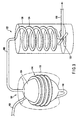
- Figure 3 contains a perspective drawing that illustrates a structure in which a heated reactor 102 and a cooler 122 are combined.
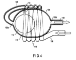
- Figure 4 contains a cross-sectional drawing that illustrates the internal structure of the essential features of the heated reactor 102 .
- This heated reactor 102 and cooler 122 can be used for the heated reactor 44 and cooler 46 in the apparatus illustrated in Figure 1 and for the heated reactor 84 and cooler 86 in the apparatus illustrated in Figure 2.
- the heater 102 is provided with a reaction chamber 104 that is formed by an oval-shaped casing and that has a first port 105a and a second port 105b .
- the upstream conduit 106 is connected to the first port 105a in order to introduce a mixed gas of chlorine gas, fluorine gas, and inert gas.
- the downstream conduit 108 is connected to the second port 105b in order to withdraw the gas produced by the reaction chamber 104 .
- a baffle member 112 is disposed within the reaction chamber 104 facing the first port 105a . This baffle member 112 is composed of a spherical element and is fixed by welding through a suitable spacer 113 to the inner surface of the reaction chamber 104 .
- the combination of the oval shape of the reaction chamber 104 and the spherical shape of the baffle member 112 functions to stop the generation of gas drift (gas stagnation) in the reaction chamber 104 .
- the reaction chamber 104 , the conduits 106 and 108 , the baffle member 112 , and the spacer 113 are composed of highly thermoconductive material that is strongly resistant to corrosion by CIF 3 , for example, Ni.
- the cooler 122 is provided with a coil 124 formed by the spiral coiling of the downstream conduit 108 .
- This coil 124 is held within a cylindrical casing 126 , and a fan 128 is disposed at the port at the lower end thereof.
- the cooler 122 has an air-cooled structure in which the gas in the coil 124 is cooled to around room temperature by the fan.
- this invention because it enables the onsite and on-demand supply of IFCG-containing product gas, can improve the safety, cost, and flexibility of the cleaning methods and apparatuses and etching methods and apparatuses in semiconductor processing systems.
Landscapes
- Chemical & Material Sciences (AREA)
- General Chemical & Material Sciences (AREA)
- Chemical Kinetics & Catalysis (AREA)
- Engineering & Computer Science (AREA)
- Materials Engineering (AREA)
- Mechanical Engineering (AREA)
- Metallurgy (AREA)
- Organic Chemistry (AREA)
- Electrochemistry (AREA)
- Physics & Mathematics (AREA)
- Optics & Photonics (AREA)
- Drying Of Semiconductors (AREA)
Abstract
Description
- This invention relates to a cleaning method and apparatus and an etching method and apparatus for semiconductor processing systems wherein said cleaning method and apparatus and said etching method and apparatus use an interhalogen fluorine compound gas (IFCG). Here, semiconductor processing denotes the various processes that are executed in order to fabricate a semiconductor device - or a structure that connects to a semiconductor device - on a treatment substrate through the formation thereon of a semiconductor layer, insulating layer, conductive layer, etc., in a prescribed pattern. Said treatment substrate can be, for example, a semiconductor wafer or an LCD substrate, and the connecting structure can be, for example, a conductor, trace, or electrode.
- Interhalogen fluorine compound gases, such as CIF3, are used in semiconductor processing systems to etch treatment substrates and to clean the treating chambers and exhaust pipe systems. For example, CIF3 (chlorine trifluoride) gas is utilized as a cleaning gas for the CVD equipment that is used to form films of silicon (Si), polysilicon, amorphous silicon, silicon oxide (SiO2), silicon nitride (Si3N4), tungsten silicide (WSi2), titanium-tungsten (TiW), tantalum oxide (Ta2O5), and silicon-germanium (SiGe). An advantage of CIF3 gas is its ability to react without using a plasma; depending on the particular case, it will react even at ambient temperature.
- CIF3 gas is filled as a high-purity liquefied gas into metal cylinders and is delivered in this form to the user's site. At the user's site, the gas-phase portion of the CIF3 is withdrawn from the cylinder, is depressurized to the vapor pressure prevailing at the cylinder temperature at this point (or to below this vapor pressure), and is then transported to the particular semiconductor fabrication apparatus.
- Since CIF3 has a low boiling point at 12°C, a precise temperature control must be exercised - in particular when large CIF3 gas flow rates are required - over the associated pumps and supply conduit system in order to obtain the required quantities of the gas and in order to prevent reliquefaction along the conduit pathways. However, CIF3 is very corrosive and strongly oxidizing and in particular has a very high reactivity in its liquid phase. This places limitations from a materials standpoint on the ability to heat the pumps and conduits, while at the same time heating the pumps and conduits is also undesirable from a practical standpoint. In addition, the storage and transport of this highly reactive liquefied CIF3 gas is tightly regulated in the United States and Europe, which places limitations on its range of applications notwithstanding the fact that it is a highly desirable cleaning gas.
- In another vein, since very high purity levels are not required when CIF3 is used as a cleaning gas, instances occur in which the CIF3 purity required by the user does not match the cost of CIF3 production. Moreover, depending on the particular process involved, it may be preferable to admix different components, for example, CIF or CIF5, rather than employ a process gas composed of only CIF3. Again depending on the particular process involved, it may even be desirable in some cases to make CIF or CIF5 the main component. At the present time, a means such as the addition of a separate process for producing the process gas is required when it is desired to make these types of adjustments in the gas components as a function of the particular process.
- This invention was developed in view of the problems described above for the prior art. The object of this invention is to provide improvements in the safety, cost, and flexibility of the IFCG-based cleaning methods and apparatuses and IFCG-based etching methods and apparatuses that are used in semiconductor processing systems.
- This invention, which achieves the aforesaid object, is essentially characterized by the onsite and on-demand production and supply of IFCG. For the present purposes, onsite means that the IFCG-producing mechanism is combined with the main processing mechanism of the semiconductor processing system. On-demand is taken to mean that the process gas can be supplied in accordance with the timing required by the main processing mechanism and in accordance with any component adjustment required by the main processing mechanism.
- A first aspect of this invention is a cleaning method that removes by-product containing material selected from the group consisting of Si, Mo, Ta, W, SiOx, SiNx, SiON, SiC, SiGe, TaSix, TaOx, WSix, TiC, TiN, TiW, BN, and indium tin oxide (ITO), that has accumulated in the treating chamber of a semiconductor processing system, wherein said cleaning method is provided with
a process comprising the formation of a mixed gas by mixing the gases afforded by independently introducing a nonfluorine first halogen gas and fluorine gas from, respectively, a first gas source and a second gas source, and selectively introducing inert gas from a third gas source, and
a process in which a product gas containing IFCG is produced by feeding the aforesaid mixed gas into a heated reactor and heating said mixed gas to a temperature at which the first halogen gas and fluorine gas react, and in which said product gas is fed concurrent with its production into the aforesaid treating chamber. - According to a second aspect of this invention, the first halogen gas : fluorine gas : inert gas volumetric ratio in the mixed gas in the method of the first aspect is established at 10 - 90: 10 - 90 : 0 - 90.
- According to a third aspect of this invention, in the method of the first or second aspect, the first halogen gas is chlorine gas and the temperature to which the mixed gas is heated by the aforesaid heated reactor is 200°C to 400°C.
- According to a fourth aspect of this invention, the aforesaid inert gas in the method of the first, second, or third aspect is helium.
- A fifth aspect of this invention comprises a cleaning apparatus that removes by-product containing material selected from the group consisting of Si, Mo, Ta, W, SiOx, SiNx, SiON, SiC, SiGe, TaSix, TaOx, WSix, TiC, TiN, TiW, BN, and ITO, that has accumulated in the treating chamber of a semiconductor processing system, wherein said cleaning apparatus is provided with
an upstream section that forms a mixed gas by mixing the gases afforded by the independent introduction of a nonfluorine first halogen gas and fluorine gas from, respectively, a first gas source and a second gas source, and the selective introduction of inert gas from a third gas source, and
a downstream section that produces a product gas containing IFCG by feeding the aforesaid mixed gas into a heated reactor and heating said mixed gas to a temperature at which the first halogen gas and fluorine gas react, and that feeds said product gas concurrent with its production into the aforesaid treating chamber. - According to a sixth aspect of this invention, the upstream section in the apparatus of the fifth aspect is provided with a controller that can vary the first halogen gas : fluorine gas : inert gas volumetric ratio in the aforesaid mixed gas through independent adjustment of the individual flow rates of the first halogen gas, fluorine gas, and inert gas.
- According to a seventh aspect of this invention, the heated reactor in the apparatus of the fifth or sixth aspect is provided with a reaction chamber and an upstream conduit that introduces the aforesaid mixed gas into said reaction chamber, wherein said reaction chamber and said upstream conduit are composed of a highly thermoconductive material that is highly resistant to corrosion by the aforesaid product gas, the aforesaid upstream conduit forms a heat-exchange section by wrapping around the aforesaid periphery, and said heat-exchange section is heated from the periphery by a heater.
- An eighth aspect of this invention comprises a method for etching in a semiconductor processing system, that etches a first film on a treatment substrate, said first film substantially comprising material selected from the group consisting of Si, SIPOS (semi-insulating polycrystalline silicon), Ta, and TaSix, wherein said etching method is provided with
a process comprising the formation of a mixed gas by mixing the gases afforded by independently introducing a nonfluorine first halogen gas and fluorine gas from, respectively, a first gas source and a second gas source, and selectively introducing inert gas from a third gas source, and
a process in which a product gas containing IFCG is produced by feeding the aforesaid mixed gas into a heated reactor and heating said mixed gas to a temperature at which the first halogen gas and fluorine gas react, and in which said product gas is fed concurrent with its production into the aforesaid treating chamber. - According to a ninth aspect of this invention, a second film is present in the method of the eighth aspect on the aforesaid treatment substrate, wherein said second film substantially comprises material selected from the group consisting of SiO2, SiNx, SiON, TaOx, and photoresists and the aforesaid etching method etches the aforesaid first film selectively relative to the said second film.
- A tenth aspect of this invention is an etching apparatus in a semiconductor processing system, that etches a first film on a treatment substrate, said first film substantially comprising material selected from the group consisting of Si, SIPOS, Ta, and TaSix, wherein said etching apparatus is provided with
a treating chamber that holds the aforesaid treatment substrate,
an upstream section that forms a mixed gas by mixing the gases afforded by the independent introduction of a nonfluorine first halogen gas and fluorine gas from, respectively, a first gas source and a second gas source, and the selective introduction of inert gas from a third gas source, and
a downstream section that produces a product gas containing IFCG by feeding the aforesaid mixed gas into a heated reactor and heating said mixed gas to a temperature at which the first halogen gas and fluorine gas react, and that feeds said product gas concurrent with its production into the aforesaid treating chamber. - According to an eleventh aspect of this invention, the heated reactor in the apparatus of the tenth aspect is provided with a reaction chamber and an upstream conduit that introduces the aforesaid mixed gas into said reaction chamber, wherein said reaction chamber and said upstream conduit are composed of a highly thermoconductive material that is highly resistant to corrosion by the aforesaid product gas, the aforesaid upstream conduit forms a heat-exchange section by wrapping around the aforesaid periphery, and said heat-exchange section is heated from the periphery by a heater.
-
- Figure 1 contains a schematic drawing that illustrates a cleaning apparatus that is an embodiment of the present invention. This cleaning apparatus removes by-product that has accumulated within the treating chamber of a semiconductor processing system.
- Figure 2 contains a schematic drawing that illustrates, as another embodiment of the present invention, an etching apparatus in a semiconductor processing system.
- Figure 3 contains a perspective drawing that illustrates a heated reactor/cooler combined structure that is usable in the apparatuses shown in Figures 1 and 2.
- Figure 4 contains a cross-sectional drawing that illustrates the internal structure of the essential features of the heated reactor shown in Figure 3.
- Figure 1 contains a schematic drawing of a cleaning apparatus that is an embodiment of this invention and that removes by-product that has accumulated within the treating chamber of a semiconductor processing system. This
cleaning apparatus 30 may be connected to, for example, a CVD apparatus 10 set up to form a silicon film on a treatment substrate, e.g., a semiconductor wafer or LCD substrate. - The CVD apparatus 10 is provided with a treating
chamber 12 that holds the treatment substrate. Disposed within the treatingchamber 12 is aplatform 14 for mounting the treatment substrate. The lower region of the treatingchamber 12 is connected to anexhaust system 16 that exhausts the interior and establishes a vacuum therein. The upper region of the treatingchamber 12 is connected to afeed system 18 that supplies process gas, for example, SiH4. - The repetition of film-forming processes in such a CVD apparatus 10 causes the accumulation of by-product (main component = Si) on the inner walls of the treating
chamber 12 and the inner walls of the conduits of theexhaust system 16. Thecleaning apparatus 30 in accordance with this invention is used to remove this by-product. - The
cleaning apparatus 30 is provided with afirst gas source 32, asecond gas source 34, and athird gas source 36 in order to supply, respectively, chlorine (Cl2) gas, fluorine (F2) gas, and inert gas. Thechlorine gas source 32 comprises a cylinder filled with the liquefied gas. Feed of the chlorine gas is relatively easy due to the high vapor pressure involved. The fluorinesecond gas source 34, on the other hand, comprises a gas generator that produces fluorine gas by electrolysis, although the fluorine gas could also be supplied as a high-pressure gas from a cylinder. - The inert gas functions as a diluent gas or carrier gas, and any inert gas can be used, e.g., helium, argon, nitrogen, and so forth. However, the use of helium with its high thermal conductivity is particularly preferred in order to facilitate heating of the mixed gas, vide infra. Use of the inert gas may be omitted depending on the particular treatment, i.e., introduction of the inert gas is carried out on a selective basis.
- The chlorine gas from the
first gas source 32, the fluorine gas from thesecond gas source 34, and the inert gas from thethird gas source 36 pass through, respectively, mass flow controller (MFC) 38a,MFC 38b, andMFC 38c, which results in their introduction with their flow rates under separate and independent control. The independently introduced chlorine gas, fluorine gas, and inert gas are combined and mixed in theconduit 42 to form a mixed gas. The chlorine gas : fluorine gas : inert gas volumetric ratio established in this mixed gas should be 10 - 90 : 10 - 90 : 0 - 90. - The mixed gas generated in this manner is transported into a
heated reactor 44, for example, a heat exchanger, and is heated to 200°C to 400° and preferably 250°C to 350°C. This serves to produce a product gas containing chlorine fluoride gas, e.g., CIF3 gas, through reaction of the chlorine gas and fluorine gas. This product gas, which will contain CIF3 gas as its main component along with other chlorine fluoride gases (CIF, CIF5, etc.), by-products, and unreacted gases, is cooled by the cooler 46 to around room temperature - where CIF3 does not liquefy - and is discharged at a pressure at which the CIF3 does not liquefy. - The product gas withdrawn from the cooler 46 is first passed through an
analyzer 48 that measures the interhalogen fluorine compound. The measurement results afforded by theanalyzer 48 are fedback to themain controller 52, and theMFCs - The flow rate and pressure of the product gas are then adjusted in the
buffer 54 so as to compatibilize these parameters with the conditions in the treatingchamber 12 of the CVD apparatus 10. After this adjustment the product gas is fed to the treatingchamber 12. Thebuffer 54 can also be executed as a temporary storage section that carries out liquefaction of the product gas and its ensuing re-volatilization. This enables the removal of solids and unreacted volatile gases, gaseous by-products, and impurity gases from the product gas in thebuffer 54. The chlorine fluoride gas (e.g., CIF3 gas) in the product gas fed into the treatingchamber 12 reacts with the by-product (main component = Si) that has accumulated on the inner walls of the treatingchamber 12 and the inner walls of theexhaust system 16 and thereby debonds same from these inner walls. The debonded by-product becomes entrained in the exhaust flow produced by the action of theexhaust system 16 and is flushed from the CVD apparatus 10. - While the embodiment under consideration involves the combination of the
cleaning apparatus 30 with a silicon CVD apparatus 10, chlorine fluoride gas is also effective for the removal of substances other than silicon (silicon includes polysilicon and amorphous silicon). These substances other than silicon can be specifically exemplified by Mo, Ta, W, SiOx, SiNx, SiON, SiC, SiGe, TaSix, TaOx, WSix, TiC, TiN, TiW, BN, and ITO. Thus, thecleaning apparatus 30 can be effectively used for the cleaning, inter alia, of CVD equipment and etching equipment in which by-product containing material selected from the aforesaid material group has been produced by the particular primary process implemented in the equipment. - A mixed gas of 30 SCCM chlorine gas, 100 SCCM fluorine gas, and 100 SCCM helium was produced and continuously fed at an internal system pressure of 836 torr into a
heated reactor 44 comprising a nickel heat exchanger heated to 250°C to 350°C. As a result, a product gas was obtained that in the vicinity of the outlet from theheated reactor 44 had a CIF3 concentration of 10% to 30%, giving a CIF3 yield of 60% to 80%. - Figure 2 contains a schematic drawing of an etching apparatus that is another embodiment of this invention, said etching apparatus residing in a semiconductor processing system. This
etching apparatus 60 can be used, for example, to etch an Si film on a treatment substrate in preference to an SiO2 film (selective etching). The treatment substrate can be, for example, a semiconductor wafer or LCD substrate. - The
etching apparatus 60 is provided with a treatingchamber 62 that holds the treatment substrate. Disposed within the treatingchamber 62 is aplatform 64 for mounting the treatment substrate. The lower region of the treatingchamber 62 is connected to anexhaust system 66 that exhausts the interior and establishes a vacuum therein. The upper region of the treatingchamber 62 is connected to afeed system 70 that supplies etching gas. Thefeed system 70 in theetching apparatus 60 has the same structure as thecleaning apparatus 30 that is illustrated in Figure 1. - More specifically, this
feed system 70 is provided with afirst gas source 72, asecond gas source 74, and athird gas source 76 in order to supply, respectively, chlorine (Cl2) gas, fluorine (F2) gas, and inert gas. The chlorine gas from thefirst gas source 72, the fluorine gas from thesecond gas source 74, and the inert gas from thethird gas source 76 pass through, respectively,MFC 78a,MFC 78b, andMFC 78c, which results in their introduction with their flow rates under separate and independent control. The independently introduced chlorine gas, fluorine gas, and inert gas are combined and mixed in theconduit 82 to form a mixed gas. The chlorine gas : fluorine gas : inert gas volumetric ratio established in this mixed gas should be 10 - 90 : 10 - 90 : 0 - 90. - The mixed gas generated in this manner is transported into a
heated reactor 84, for example, a heat exchanger, and is heated to 200°C to 400°C and preferably 250°C to 350°C. This serves to produce a product gas containing chlorine fluoride gas, e.g., CIF3 gas, through reaction of the chlorine gas and fluorine gas. This product gas, which will contain CIF3 gas as its main component along with other chlorine fluoride gases (CIF, CIF5, etc.), by-products, and unreacted gases, is cooled by the cooler 86 to around room temperature - where CIF3 does not liquefy - and is discharged at a pressure at which the CIF3 does not liquefy. - The product gas withdrawn from the cooler 86 is first passed through an
analyzer 88 that measures the interhalogen fluorine compound. The measurement results afforded by theanalyzer 88 are fedback to themain controller 92, and theMFCs - The flow rate and pressure of the product gas are then adjusted in the
buffer 94 so as to compatibilize these parameters with the conditions prevailing in the treatingchamber 12 of the CVD apparatus 10. After this adjustment the product gas is fed to the treatingchamber 12. Thebuffer 94 can also be executed as a temporary storage section that carries out liquefaction of the product gas and its ensuing re-volatilization. This enables the removal of solids and unreacted volatile gases, gaseous by-products, and impurity gases from the product gas in thebuffer 94. The chlorine fluoride gas (e.g., CIF3 gas) in the product gas fed into the treatingchamber 62 reacts with Si film on the treatment substrate in preference to SiO2 film on the treatment substrate, thereby etching the former. The etching product becomes entrained in the exhaust flow produced by the action of theexhaust system 66 and is flushed from theetching apparatus 60. - In the embodiment under consideration, the
etching apparatus 60 has been styled as an apparatus for etching a first film comprising Si film on a treatment substrate selectively with respect to a second film comprising SiO2 film. However, chlorine fluoride gas is also effective for the selective etching of material combinations other than the Si film/SiO2 film combination. Specifically, the first film, i.e., the film that is preferentially etched, can substantially comprise material selected from the group consisting of Si, SIPOS, Ta, and TaSix. The second film, i.e., the film that is not preferentially etched, can substantially comprise material selected from the group consisting of SiO2, SiNx, SiON, TaOx, and photoresists. - The
cleaning apparatus 30 and theetching apparatus 60 described in the preceding have the ability to both produce and supply chlorine fluoride gas, e.g., CIF3 gas, at the user's site using chlorine gas, fluorine gas, and inert gas as gas sources. This extinguishes the operational and regulatory problems associated with the supply of chlorine fluoride gas, e.g., CIF3 gas, to the user's site as a liquefied gas in cylinders. More particularly, theapparatuses - Other types of interhalogen fluorine compound gases can be generated and supplied by using another halogen gas (other than fluorine) in place of chlorine gas as the gas in the first gas source (32, 72). For example, the use of bromine (Br2) gas as the gas in the
first gas source 32 enables the supply of product gas containing at least 1 of BrF, BrF3, and BrF5, while the use of iodine (I2) gas as the gas in thefirst gas source 32 enables the supply of product gas containing at least 1 of IF, IF3, IF5, and IF7. An appropriate process pressure and temperature should be selected in correspondence to the source gas used when the production and supply of these other IFCGs is being pursued. - Figure 3 contains a perspective drawing that illustrates a structure in which a
heated reactor 102 and a cooler 122 are combined. Figure 4 contains a cross-sectional drawing that illustrates the internal structure of the essential features of theheated reactor 102. Thisheated reactor 102 and cooler 122 can be used for theheated reactor 44 and cooler 46 in the apparatus illustrated in Figure 1 and for theheated reactor 84 and cooler 86 in the apparatus illustrated in Figure 2. - The
heater 102 is provided with areaction chamber 104 that is formed by an oval-shaped casing and that has afirst port 105a and asecond port 105b. Theupstream conduit 106 is connected to thefirst port 105a in order to introduce a mixed gas of chlorine gas, fluorine gas, and inert gas. Thedownstream conduit 108 is connected to thesecond port 105b in order to withdraw the gas produced by thereaction chamber 104. Abaffle member 112 is disposed within thereaction chamber 104 facing thefirst port 105a. Thisbaffle member 112 is composed of a spherical element and is fixed by welding through asuitable spacer 113 to the inner surface of thereaction chamber 104. The combination of the oval shape of thereaction chamber 104 and the spherical shape of thebaffle member 112 functions to stop the generation of gas drift (gas stagnation) in thereaction chamber 104. Thereaction chamber 104, theconduits baffle member 112, and thespacer 113 are composed of highly thermoconductive material that is strongly resistant to corrosion by CIF3, for example, Ni. - The
upstream conduit 106 wraps the periphery of thereaction chamber 104 to form aheat exchanger 114. Thisheat exchanger 114 is also completely enveloped by ajacket heater 116 and is heated from the periphery. Thejacket heater 116 comprises an electrically controlled fabric-type heater comprising resistance heating wire embedded in heat-resistant nonwoven fabric. - The cooler 122 is provided with a
coil 124 formed by the spiral coiling of thedownstream conduit 108. Thiscoil 124 is held within acylindrical casing 126, and afan 128 is disposed at the port at the lower end thereof. Thus, the cooler 122 has an air-cooled structure in which the gas in thecoil 124 is cooled to around room temperature by the fan. - The integral formation of the
heat exchanger 114 on the periphery of thereaction chamber 104 in accordance with theheated reactor 102 illustrated in Figures 3 and 4 enables the size of the reactor to be reduced and enables a good thermal efficiency to be obtained. - As has been explained in detail in the preceding, this invention, because it enables the onsite and on-demand supply of IFCG-containing product gas, can improve the safety, cost, and flexibility of the cleaning methods and apparatuses and etching methods and apparatuses in semiconductor processing systems.
Claims (11)
- Cleaning method that removes by-product containing material selected from the group consisting of Si, Mo, Ta, W, SiOx, SiNx, SiON, SiC, SiGe, TaSix, TaOx, WSix, TiC, TiN, TiW, BN, and ITO, that has accumulated in the treating chamber of a semiconductor processing system, wherein said cleaning method is provided with
a process comprising the formation of a mixed gas by mixing the gases afforded by independently introducing a nonfluorine first halogen gas and fluorine gas from, respectively, a first gas source and a second gas source, and selectively introducing inert gas from a third gas source, and
a process in which a product gas containing an interhalogen fluorine compound gas is produced by feeding the aforesaid mixed gas into a heated reactor and heating said mixed gas to a temperature at which the first halogen gas and fluorine gas react, and in which said product gas is fed concurrent with its production into the aforesaid treating chamber. - The method described in Claim 1, in which the first halogen gas : fluorine gas : inert gas volumetric ratio established in the mixed gas is 10 - 90 10 - 90 : 0 - 90.
- The method described in Claim 1 or 2, in which the first halogen gas is chlorine gas and the temperature to which the aforesaid mixed gas is heated by the aforesaid heated reactor is 200°C to 400°C.
- The method described in any of Claims 1 through 3, in which the inert gas is helium.
- Cleaning apparatus that removes by-product containing material selected from the group consisting of Si, Mo, Ta, W, SiOx, SiNx, SiON, SiC, SiGe, TaSix, TaOx, WSix, TiC, TiN, TiW, BN, and ITO, that has accumulated in the treating chamber of a semiconductor processing system, wherein said cleaning apparatus is provided with
an upstream section that forms a mixed gas by mixing the gases afforded by the independent introduction of a nonfluorine first halogen gas and fluorine gas from, respectively, a first gas source and a second gas source, and the selective introduction of inert gas from a third gas source, and
a downstream section that produces a product gas containing an interhalogen fluorine compound gas by feeding the aforesaid mixed gas into a heated reactor and heating said mixed gas to a temperature at which the first halogen gas and fluorine gas react, and that feeds said product gas concurrent with its production into the aforesaid treating chamber. - The apparatus described in Claim 5, in which the aforesaid upstream section is provided with a controller that can vary the first halogen gas : fluorine gas : inert gas volumetric ratio in the aforesaid mixed gas through independent adjustment of the individual flow rates of the first halogen gas, fluorine gas, and inert gas.
- The apparatus described in Claim 5 or 6, in which the aforesaid heated reactor is provided with a reaction chamber and an upstream conduit that introduces the aforesaid mixed gas into said reaction chamber, wherein said reaction chamber and said upstream conduit are composed of a highly thermoconductive material that is highly resistant to corrosion by the aforesaid product gas, the aforesaid upstream conduit forms a heat-exchange section by wrapping around the aforesaid periphery, and said heat-exchange section is heated from the periphery by a heater.
- Method for etching in a semiconductor processing system, that etches a first film on a treatment substrate, said first film being substantially composed of material selected from the group consisting of Si, SIPOS, Ta, and TaSix, wherein said etching method is provided with
a process comprising the formation of a mixed gas by mixing the gases afforded by independently introducing a nonfluorine first halogen gas and fluorine gas from, respectively, a first gas source and a second gas source, and selectively introducing inert gas from a third gas source, and
a process in which a product gas containing an interhalogen fluorine compound gas is produced by feeding the aforesaid mixed gas into a heated reactor and heating said mixed gas to a temperature at which the first halogen gas and fluorine gas react, and in which said product gas is fed concurrent with its production into the aforesaid treating chamber. - The method described in Claim 8, in which a second film is present on the aforesaid treatment substrate, wherein said second film is substantially composed of material selected from the group consisting of SiO2, SiNx, SiON, TaOx, and photoresists and the aforesaid etching method etches the aforesaid first film selectively relative to said second film.
- Etching apparatus in a semiconductor processing system, that etches a first film on a treatment substrate, said first film being substantially composed of material selected from the group consisting of Si, SIPOS, Ta, and TaSix, wherein said etching apparatus is provided with
a treating chamber that holds the aforesaid treatment substrate,
an upstream section that forms a mixed gas by mixing the gases afforded by the independent introduction of a nonfluorine first halogen gas and fluorine gas from, respectively, a first gas source and a second gas source, and the selective introduction of inert gas from a third gas source, and
a downstream section that produces a product gas containing an interhalogen fluorine compound gas by feeding the aforesaid mixed gas into a heated reactor and heating said mixed gas to a temperature at which the first halogen gas and fluorine gas react, and that feeds said product gas concurrent with its production into the aforesaid treating chamber. - The apparatus described in Claim 10, in which the aforesaid heated reactor is provided with a reaction chamber and an upstream conduit that introduces the aforesaid mixed gas into said reaction chamber, wherein said reaction chamber and said upstream conduit are composed of a highly thermoconductive material that is highly resistant to corrosion by the aforesaid product gas, the aforesaid upstream conduit forms a heat-exchange section by wrapping around the aforesaid periphery, and said heat-exchange section is heated from the periphery by a heater.
Applications Claiming Priority (1)
| Application Number | Priority Date | Filing Date | Title |
|---|---|---|---|
| PCT/JP2001/006604 WO2003012843A1 (en) | 2001-07-31 | 2001-07-31 | Method and apparatus for cleaning and method and apparatus for etching |
Publications (2)
| Publication Number | Publication Date |
|---|---|
| EP1460678A1 true EP1460678A1 (en) | 2004-09-22 |
| EP1460678A4 EP1460678A4 (en) | 2010-01-06 |
Family
ID=11737608
Family Applications (1)
| Application Number | Title | Priority Date | Filing Date |
|---|---|---|---|
| EP01954400A Withdrawn EP1460678A4 (en) | 2001-07-31 | 2001-07-31 | CLEANING METHOD AND APPARATUS AND METHOD AND APPARATUS FOR ETCHING |
Country Status (3)
| Country | Link |
|---|---|
| US (1) | US20050020071A1 (en) |
| EP (1) | EP1460678A4 (en) |
| WO (1) | WO2003012843A1 (en) |
Cited By (2)
| Publication number | Priority date | Publication date | Assignee | Title |
|---|---|---|---|---|
| EP1538235A1 (en) * | 2003-11-26 | 2005-06-08 | Air Products And Chemicals, Inc. | Method for etching high dielectric constant materials and for cleaning deposition chambers for high dielectric constant materials |
| WO2010115734A1 (en) * | 2009-04-01 | 2010-10-14 | Solvay Fluor Gmbh | Process for the manufacture of etched items |
Families Citing this family (423)
| Publication number | Priority date | Publication date | Assignee | Title |
|---|---|---|---|---|
| US20040011380A1 (en) * | 2002-07-18 | 2004-01-22 | Bing Ji | Method for etching high dielectric constant materials and for cleaning deposition chambers for high dielectric constant materials |
| US20100012153A1 (en) * | 2006-07-27 | 2010-01-21 | Takamitsu Shigemoto | Method of cleaning film forming apparatus and film forming apparatus |
| US8986456B2 (en) * | 2006-10-10 | 2015-03-24 | Asm America, Inc. | Precursor delivery system |
| US20100112191A1 (en) * | 2008-10-30 | 2010-05-06 | Micron Technology, Inc. | Systems and associated methods for depositing materials |
| US10378106B2 (en) | 2008-11-14 | 2019-08-13 | Asm Ip Holding B.V. | Method of forming insulation film by modified PEALD |
| US20100159122A1 (en) * | 2008-12-19 | 2010-06-24 | Canon Kabushiki Kaisha | Deposition film forming apparatus, deposition film forming method and electrophotographic photosensitive member manufacturing method |
| JP5521372B2 (en) * | 2009-04-03 | 2014-06-11 | セントラル硝子株式会社 | In-situ gas mixing and dilution system for fluorine gas |
| US9394608B2 (en) | 2009-04-06 | 2016-07-19 | Asm America, Inc. | Semiconductor processing reactor and components thereof |
| US8883270B2 (en) * | 2009-08-14 | 2014-11-11 | Asm America, Inc. | Systems and methods for thin-film deposition of metal oxides using excited nitrogen—oxygen species |
| US8802201B2 (en) | 2009-08-14 | 2014-08-12 | Asm America, Inc. | Systems and methods for thin-film deposition of metal oxides using excited nitrogen-oxygen species |
| US8877655B2 (en) | 2010-05-07 | 2014-11-04 | Asm America, Inc. | Systems and methods for thin-film deposition of metal oxides using excited nitrogen-oxygen species |
| CN102002686A (en) * | 2010-11-02 | 2011-04-06 | 深圳市华星光电技术有限公司 | Chemical vapor deposition equipment and cooling tank thereof |
| US9312155B2 (en) | 2011-06-06 | 2016-04-12 | Asm Japan K.K. | High-throughput semiconductor-processing apparatus equipped with multiple dual-chamber modules |
| KR20120140148A (en) * | 2011-06-20 | 2012-12-28 | 엘지이노텍 주식회사 | Deposition apparatus and method for forming thin film |
| US9793148B2 (en) | 2011-06-22 | 2017-10-17 | Asm Japan K.K. | Method for positioning wafers in multiple wafer transport |
| US10364496B2 (en) | 2011-06-27 | 2019-07-30 | Asm Ip Holding B.V. | Dual section module having shared and unshared mass flow controllers |
| US10854498B2 (en) | 2011-07-15 | 2020-12-01 | Asm Ip Holding B.V. | Wafer-supporting device and method for producing same |
| US20130023129A1 (en) | 2011-07-20 | 2013-01-24 | Asm America, Inc. | Pressure transmitter for a semiconductor processing environment |
| US9341296B2 (en) | 2011-10-27 | 2016-05-17 | Asm America, Inc. | Heater jacket for a fluid line |
| US9096931B2 (en) | 2011-10-27 | 2015-08-04 | Asm America, Inc | Deposition valve assembly and method of heating the same |
| US9017481B1 (en) | 2011-10-28 | 2015-04-28 | Asm America, Inc. | Process feed management for semiconductor substrate processing |
| US9005539B2 (en) | 2011-11-23 | 2015-04-14 | Asm Ip Holding B.V. | Chamber sealing member |
| US9167625B2 (en) | 2011-11-23 | 2015-10-20 | Asm Ip Holding B.V. | Radiation shielding for a substrate holder |
| US9202727B2 (en) | 2012-03-02 | 2015-12-01 | ASM IP Holding | Susceptor heater shim |
| US8946830B2 (en) | 2012-04-04 | 2015-02-03 | Asm Ip Holdings B.V. | Metal oxide protective layer for a semiconductor device |
| TWI622664B (en) | 2012-05-02 | 2018-05-01 | Asm智慧財產控股公司 | Phase stable film, structure and device comprising the same, and method of forming same |
| US8728832B2 (en) | 2012-05-07 | 2014-05-20 | Asm Ip Holdings B.V. | Semiconductor device dielectric interface layer |
| US8933375B2 (en) | 2012-06-27 | 2015-01-13 | Asm Ip Holding B.V. | Susceptor heater and method of heating a substrate |
| US9558931B2 (en) | 2012-07-27 | 2017-01-31 | Asm Ip Holding B.V. | System and method for gas-phase sulfur passivation of a semiconductor surface |
| US9117866B2 (en) | 2012-07-31 | 2015-08-25 | Asm Ip Holding B.V. | Apparatus and method for calculating a wafer position in a processing chamber under process conditions |
| US9169975B2 (en) | 2012-08-28 | 2015-10-27 | Asm Ip Holding B.V. | Systems and methods for mass flow controller verification |
| US9659799B2 (en) | 2012-08-28 | 2017-05-23 | Asm Ip Holding B.V. | Systems and methods for dynamic semiconductor process scheduling |
| US9021985B2 (en) | 2012-09-12 | 2015-05-05 | Asm Ip Holdings B.V. | Process gas management for an inductively-coupled plasma deposition reactor |
| US9324811B2 (en) | 2012-09-26 | 2016-04-26 | Asm Ip Holding B.V. | Structures and devices including a tensile-stressed silicon arsenic layer and methods of forming same |
| US10714315B2 (en) | 2012-10-12 | 2020-07-14 | Asm Ip Holdings B.V. | Semiconductor reaction chamber showerhead |
| US9640416B2 (en) | 2012-12-26 | 2017-05-02 | Asm Ip Holding B.V. | Single-and dual-chamber module-attachable wafer-handling chamber |
| US20160376700A1 (en) | 2013-02-01 | 2016-12-29 | Asm Ip Holding B.V. | System for treatment of deposition reactor |
| US8894870B2 (en) | 2013-02-01 | 2014-11-25 | Asm Ip Holding B.V. | Multi-step method and apparatus for etching compounds containing a metal |
| JP6107198B2 (en) * | 2013-02-14 | 2017-04-05 | セントラル硝子株式会社 | Cleaning gas and cleaning method |
| US9589770B2 (en) | 2013-03-08 | 2017-03-07 | Asm Ip Holding B.V. | Method and systems for in-situ formation of intermediate reactive species |
| US9484191B2 (en) | 2013-03-08 | 2016-11-01 | Asm Ip Holding B.V. | Pulsed remote plasma method and system |
| US8993054B2 (en) | 2013-07-12 | 2015-03-31 | Asm Ip Holding B.V. | Method and system to reduce outgassing in a reaction chamber |
| US9018111B2 (en) | 2013-07-22 | 2015-04-28 | Asm Ip Holding B.V. | Semiconductor reaction chamber with plasma capabilities |
| US9793115B2 (en) | 2013-08-14 | 2017-10-17 | Asm Ip Holding B.V. | Structures and devices including germanium-tin films and methods of forming same |
| US9396934B2 (en) | 2013-08-14 | 2016-07-19 | Asm Ip Holding B.V. | Methods of forming films including germanium tin and structures and devices including the films |
| US9240412B2 (en) | 2013-09-27 | 2016-01-19 | Asm Ip Holding B.V. | Semiconductor structure and device and methods of forming same using selective epitaxial process |
| US9556516B2 (en) | 2013-10-09 | 2017-01-31 | ASM IP Holding B.V | Method for forming Ti-containing film by PEALD using TDMAT or TDEAT |
| US9605343B2 (en) | 2013-11-13 | 2017-03-28 | Asm Ip Holding B.V. | Method for forming conformal carbon films, structures conformal carbon film, and system of forming same |
| US10179947B2 (en) | 2013-11-26 | 2019-01-15 | Asm Ip Holding B.V. | Method for forming conformal nitrided, oxidized, or carbonized dielectric film by atomic layer deposition |
| US10683571B2 (en) | 2014-02-25 | 2020-06-16 | Asm Ip Holding B.V. | Gas supply manifold and method of supplying gases to chamber using same |
| US9447498B2 (en) | 2014-03-18 | 2016-09-20 | Asm Ip Holding B.V. | Method for performing uniform processing in gas system-sharing multiple reaction chambers |
| US10167557B2 (en) | 2014-03-18 | 2019-01-01 | Asm Ip Holding B.V. | Gas distribution system, reactor including the system, and methods of using the same |
| US11015245B2 (en) | 2014-03-19 | 2021-05-25 | Asm Ip Holding B.V. | Gas-phase reactor and system having exhaust plenum and components thereof |
| US9404587B2 (en) | 2014-04-24 | 2016-08-02 | ASM IP Holding B.V | Lockout tagout for semiconductor vacuum valve |
| US10858737B2 (en) | 2014-07-28 | 2020-12-08 | Asm Ip Holding B.V. | Showerhead assembly and components thereof |
| US9543180B2 (en) | 2014-08-01 | 2017-01-10 | Asm Ip Holding B.V. | Apparatus and method for transporting wafers between wafer carrier and process tool under vacuum |
| US9890456B2 (en) | 2014-08-21 | 2018-02-13 | Asm Ip Holding B.V. | Method and system for in situ formation of gas-phase compounds |
| KR101659560B1 (en) * | 2014-08-26 | 2016-09-23 | 주식회사 테라세미콘 | Reactor of apparatus for processing substrate |
| US10941490B2 (en) | 2014-10-07 | 2021-03-09 | Asm Ip Holding B.V. | Multiple temperature range susceptor, assembly, reactor and system including the susceptor, and methods of using the same |
| US9657845B2 (en) | 2014-10-07 | 2017-05-23 | Asm Ip Holding B.V. | Variable conductance gas distribution apparatus and method |
| KR102300403B1 (en) | 2014-11-19 | 2021-09-09 | 에이에스엠 아이피 홀딩 비.브이. | Method of depositing thin film |
| KR102263121B1 (en) | 2014-12-22 | 2021-06-09 | 에이에스엠 아이피 홀딩 비.브이. | Semiconductor device and manufacuring method thereof |
| US9478415B2 (en) | 2015-02-13 | 2016-10-25 | Asm Ip Holding B.V. | Method for forming film having low resistance and shallow junction depth |
| US10529542B2 (en) | 2015-03-11 | 2020-01-07 | Asm Ip Holdings B.V. | Cross-flow reactor and method |
| US10276355B2 (en) | 2015-03-12 | 2019-04-30 | Asm Ip Holding B.V. | Multi-zone reactor, system including the reactor, and method of using the same |
| US10458018B2 (en) | 2015-06-26 | 2019-10-29 | Asm Ip Holding B.V. | Structures including metal carbide material, devices including the structures, and methods of forming same |
| US10600673B2 (en) | 2015-07-07 | 2020-03-24 | Asm Ip Holding B.V. | Magnetic susceptor to baseplate seal |
| US9899291B2 (en) | 2015-07-13 | 2018-02-20 | Asm Ip Holding B.V. | Method for protecting layer by forming hydrocarbon-based extremely thin film |
| US10043661B2 (en) | 2015-07-13 | 2018-08-07 | Asm Ip Holding B.V. | Method for protecting layer by forming hydrocarbon-based extremely thin film |
| US10083836B2 (en) | 2015-07-24 | 2018-09-25 | Asm Ip Holding B.V. | Formation of boron-doped titanium metal films with high work function |
| US10087525B2 (en) | 2015-08-04 | 2018-10-02 | Asm Ip Holding B.V. | Variable gap hard stop design |
| US9647114B2 (en) | 2015-08-14 | 2017-05-09 | Asm Ip Holding B.V. | Methods of forming highly p-type doped germanium tin films and structures and devices including the films |
| US9711345B2 (en) | 2015-08-25 | 2017-07-18 | Asm Ip Holding B.V. | Method for forming aluminum nitride-based film by PEALD |
| US9960072B2 (en) | 2015-09-29 | 2018-05-01 | Asm Ip Holding B.V. | Variable adjustment for precise matching of multiple chamber cavity housings |
| US9909214B2 (en) | 2015-10-15 | 2018-03-06 | Asm Ip Holding B.V. | Method for depositing dielectric film in trenches by PEALD |
| US10211308B2 (en) | 2015-10-21 | 2019-02-19 | Asm Ip Holding B.V. | NbMC layers |
| US10322384B2 (en) | 2015-11-09 | 2019-06-18 | Asm Ip Holding B.V. | Counter flow mixer for process chamber |
| US9455138B1 (en) | 2015-11-10 | 2016-09-27 | Asm Ip Holding B.V. | Method for forming dielectric film in trenches by PEALD using H-containing gas |
| US9905420B2 (en) | 2015-12-01 | 2018-02-27 | Asm Ip Holding B.V. | Methods of forming silicon germanium tin films and structures and devices including the films |
| US9607837B1 (en) | 2015-12-21 | 2017-03-28 | Asm Ip Holding B.V. | Method for forming silicon oxide cap layer for solid state diffusion process |
| US9735024B2 (en) | 2015-12-28 | 2017-08-15 | Asm Ip Holding B.V. | Method of atomic layer etching using functional group-containing fluorocarbon |
| US9627221B1 (en) | 2015-12-28 | 2017-04-18 | Asm Ip Holding B.V. | Continuous process incorporating atomic layer etching |
| US11139308B2 (en) | 2015-12-29 | 2021-10-05 | Asm Ip Holding B.V. | Atomic layer deposition of III-V compounds to form V-NAND devices |
| US10529554B2 (en) | 2016-02-19 | 2020-01-07 | Asm Ip Holding B.V. | Method for forming silicon nitride film selectively on sidewalls or flat surfaces of trenches |
| US9754779B1 (en) | 2016-02-19 | 2017-09-05 | Asm Ip Holding B.V. | Method for forming silicon nitride film selectively on sidewalls or flat surfaces of trenches |
| US10468251B2 (en) | 2016-02-19 | 2019-11-05 | Asm Ip Holding B.V. | Method for forming spacers using silicon nitride film for spacer-defined multiple patterning |
| US10501866B2 (en) | 2016-03-09 | 2019-12-10 | Asm Ip Holding B.V. | Gas distribution apparatus for improved film uniformity in an epitaxial system |
| US10343920B2 (en) | 2016-03-18 | 2019-07-09 | Asm Ip Holding B.V. | Aligned carbon nanotubes |
| US9892913B2 (en) | 2016-03-24 | 2018-02-13 | Asm Ip Holding B.V. | Radial and thickness control via biased multi-port injection settings |
| EP3441362B1 (en) * | 2016-04-05 | 2025-11-26 | Kanto Denka Kogyo Co., Ltd. | Feeding process of chlorine fluoride |
| US10865475B2 (en) | 2016-04-21 | 2020-12-15 | Asm Ip Holding B.V. | Deposition of metal borides and silicides |
| US10087522B2 (en) | 2016-04-21 | 2018-10-02 | Asm Ip Holding B.V. | Deposition of metal borides |
| US10190213B2 (en) | 2016-04-21 | 2019-01-29 | Asm Ip Holding B.V. | Deposition of metal borides |
| US10367080B2 (en) | 2016-05-02 | 2019-07-30 | Asm Ip Holding B.V. | Method of forming a germanium oxynitride film |
| US10032628B2 (en) | 2016-05-02 | 2018-07-24 | Asm Ip Holding B.V. | Source/drain performance through conformal solid state doping |
| KR102592471B1 (en) | 2016-05-17 | 2023-10-20 | 에이에스엠 아이피 홀딩 비.브이. | Method of forming metal interconnection and method of fabricating semiconductor device using the same |
| US11453943B2 (en) | 2016-05-25 | 2022-09-27 | Asm Ip Holding B.V. | Method for forming carbon-containing silicon/metal oxide or nitride film by ALD using silicon precursor and hydrocarbon precursor |
| US10388509B2 (en) | 2016-06-28 | 2019-08-20 | Asm Ip Holding B.V. | Formation of epitaxial layers via dislocation filtering |
| US10612137B2 (en) | 2016-07-08 | 2020-04-07 | Asm Ip Holdings B.V. | Organic reactants for atomic layer deposition |
| US9859151B1 (en) | 2016-07-08 | 2018-01-02 | Asm Ip Holding B.V. | Selective film deposition method to form air gaps |
| US9793135B1 (en) | 2016-07-14 | 2017-10-17 | ASM IP Holding B.V | Method of cyclic dry etching using etchant film |
| US10714385B2 (en) | 2016-07-19 | 2020-07-14 | Asm Ip Holding B.V. | Selective deposition of tungsten |
| KR102354490B1 (en) | 2016-07-27 | 2022-01-21 | 에이에스엠 아이피 홀딩 비.브이. | Method of processing a substrate |
| KR102532607B1 (en) | 2016-07-28 | 2023-05-15 | 에이에스엠 아이피 홀딩 비.브이. | Substrate processing apparatus and method of operating the same |
| US10395919B2 (en) | 2016-07-28 | 2019-08-27 | Asm Ip Holding B.V. | Method and apparatus for filling a gap |
| US10177025B2 (en) | 2016-07-28 | 2019-01-08 | Asm Ip Holding B.V. | Method and apparatus for filling a gap |
| US9812320B1 (en) | 2016-07-28 | 2017-11-07 | Asm Ip Holding B.V. | Method and apparatus for filling a gap |
| US9887082B1 (en) | 2016-07-28 | 2018-02-06 | Asm Ip Holding B.V. | Method and apparatus for filling a gap |
| US10090316B2 (en) | 2016-09-01 | 2018-10-02 | Asm Ip Holding B.V. | 3D stacked multilayer semiconductor memory using doped select transistor channel |
| US10410943B2 (en) | 2016-10-13 | 2019-09-10 | Asm Ip Holding B.V. | Method for passivating a surface of a semiconductor and related systems |
| US10643826B2 (en) | 2016-10-26 | 2020-05-05 | Asm Ip Holdings B.V. | Methods for thermally calibrating reaction chambers |
| US11532757B2 (en) | 2016-10-27 | 2022-12-20 | Asm Ip Holding B.V. | Deposition of charge trapping layers |
| US10643904B2 (en) | 2016-11-01 | 2020-05-05 | Asm Ip Holdings B.V. | Methods for forming a semiconductor device and related semiconductor device structures |
| US10435790B2 (en) | 2016-11-01 | 2019-10-08 | Asm Ip Holding B.V. | Method of subatmospheric plasma-enhanced ALD using capacitively coupled electrodes with narrow gap |
| US10229833B2 (en) | 2016-11-01 | 2019-03-12 | Asm Ip Holding B.V. | Methods for forming a transition metal nitride film on a substrate by atomic layer deposition and related semiconductor device structures |
| US10714350B2 (en) | 2016-11-01 | 2020-07-14 | ASM IP Holdings, B.V. | Methods for forming a transition metal niobium nitride film on a substrate by atomic layer deposition and related semiconductor device structures |
| US10134757B2 (en) | 2016-11-07 | 2018-11-20 | Asm Ip Holding B.V. | Method of processing a substrate and a device manufactured by using the method |
| KR102546317B1 (en) | 2016-11-15 | 2023-06-21 | 에이에스엠 아이피 홀딩 비.브이. | Gas supply unit and substrate processing apparatus including the same |
| US10340135B2 (en) | 2016-11-28 | 2019-07-02 | Asm Ip Holding B.V. | Method of topologically restricted plasma-enhanced cyclic deposition of silicon or metal nitride |
| KR102762543B1 (en) | 2016-12-14 | 2025-02-05 | 에이에스엠 아이피 홀딩 비.브이. | Substrate processing apparatus |
| US9916980B1 (en) | 2016-12-15 | 2018-03-13 | Asm Ip Holding B.V. | Method of forming a structure on a substrate |
| US11447861B2 (en) | 2016-12-15 | 2022-09-20 | Asm Ip Holding B.V. | Sequential infiltration synthesis apparatus and a method of forming a patterned structure |
| US11581186B2 (en) | 2016-12-15 | 2023-02-14 | Asm Ip Holding B.V. | Sequential infiltration synthesis apparatus |
| KR102700194B1 (en) | 2016-12-19 | 2024-08-28 | 에이에스엠 아이피 홀딩 비.브이. | Substrate processing apparatus |
| US10269558B2 (en) | 2016-12-22 | 2019-04-23 | Asm Ip Holding B.V. | Method of forming a structure on a substrate |
| US10867788B2 (en) | 2016-12-28 | 2020-12-15 | Asm Ip Holding B.V. | Method of forming a structure on a substrate |
| US11390950B2 (en) | 2017-01-10 | 2022-07-19 | Asm Ip Holding B.V. | Reactor system and method to reduce residue buildup during a film deposition process |
| US10655221B2 (en) | 2017-02-09 | 2020-05-19 | Asm Ip Holding B.V. | Method for depositing oxide film by thermal ALD and PEALD |
| US10468261B2 (en) | 2017-02-15 | 2019-11-05 | Asm Ip Holding B.V. | Methods for forming a metallic film on a substrate by cyclical deposition and related semiconductor device structures |
| US10283353B2 (en) | 2017-03-29 | 2019-05-07 | Asm Ip Holding B.V. | Method of reforming insulating film deposited on substrate with recess pattern |
| US10529563B2 (en) | 2017-03-29 | 2020-01-07 | Asm Ip Holdings B.V. | Method for forming doped metal oxide films on a substrate by cyclical deposition and related semiconductor device structures |
| US10103040B1 (en) | 2017-03-31 | 2018-10-16 | Asm Ip Holding B.V. | Apparatus and method for manufacturing a semiconductor device |
| USD830981S1 (en) | 2017-04-07 | 2018-10-16 | Asm Ip Holding B.V. | Susceptor for semiconductor substrate processing apparatus |
| KR102457289B1 (en) | 2017-04-25 | 2022-10-21 | 에이에스엠 아이피 홀딩 비.브이. | Method for depositing a thin film and manufacturing a semiconductor device |
| US10770286B2 (en) | 2017-05-08 | 2020-09-08 | Asm Ip Holdings B.V. | Methods for selectively forming a silicon nitride film on a substrate and related semiconductor device structures |
| US10892156B2 (en) | 2017-05-08 | 2021-01-12 | Asm Ip Holding B.V. | Methods for forming a silicon nitride film on a substrate and related semiconductor device structures |
| US10446393B2 (en) | 2017-05-08 | 2019-10-15 | Asm Ip Holding B.V. | Methods for forming silicon-containing epitaxial layers and related semiconductor device structures |
| US10504742B2 (en) | 2017-05-31 | 2019-12-10 | Asm Ip Holding B.V. | Method of atomic layer etching using hydrogen plasma |
| US10886123B2 (en) | 2017-06-02 | 2021-01-05 | Asm Ip Holding B.V. | Methods for forming low temperature semiconductor layers and related semiconductor device structures |
| US12040200B2 (en) | 2017-06-20 | 2024-07-16 | Asm Ip Holding B.V. | Semiconductor processing apparatus and methods for calibrating a semiconductor processing apparatus |
| US11306395B2 (en) | 2017-06-28 | 2022-04-19 | Asm Ip Holding B.V. | Methods for depositing a transition metal nitride film on a substrate by atomic layer deposition and related deposition apparatus |
| US10685834B2 (en) | 2017-07-05 | 2020-06-16 | Asm Ip Holdings B.V. | Methods for forming a silicon germanium tin layer and related semiconductor device structures |
| TWI794238B (en) | 2017-07-13 | 2023-03-01 | 荷蘭商Asm智慧財產控股公司 | Apparatus and method for removal of oxide and carbon from semiconductor films in a single processing chamber |
| KR20190009245A (en) | 2017-07-18 | 2019-01-28 | 에이에스엠 아이피 홀딩 비.브이. | Methods for forming a semiconductor device structure and related semiconductor device structures |
| US10541333B2 (en) | 2017-07-19 | 2020-01-21 | Asm Ip Holding B.V. | Method for depositing a group IV semiconductor and related semiconductor device structures |
| US11374112B2 (en) | 2017-07-19 | 2022-06-28 | Asm Ip Holding B.V. | Method for depositing a group IV semiconductor and related semiconductor device structures |
| US11018002B2 (en) | 2017-07-19 | 2021-05-25 | Asm Ip Holding B.V. | Method for selectively depositing a Group IV semiconductor and related semiconductor device structures |
| US10605530B2 (en) | 2017-07-26 | 2020-03-31 | Asm Ip Holding B.V. | Assembly of a liner and a flange for a vertical furnace as well as the liner and the vertical furnace |
| US10312055B2 (en) | 2017-07-26 | 2019-06-04 | Asm Ip Holding B.V. | Method of depositing film by PEALD using negative bias |
| US10590535B2 (en) | 2017-07-26 | 2020-03-17 | Asm Ip Holdings B.V. | Chemical treatment, deposition and/or infiltration apparatus and method for using the same |
| TWI815813B (en) | 2017-08-04 | 2023-09-21 | 荷蘭商Asm智慧財產控股公司 | Showerhead assembly for distributing a gas within a reaction chamber |
| US10692741B2 (en) | 2017-08-08 | 2020-06-23 | Asm Ip Holdings B.V. | Radiation shield |
| US10770336B2 (en) | 2017-08-08 | 2020-09-08 | Asm Ip Holding B.V. | Substrate lift mechanism and reactor including same |
| US11769682B2 (en) | 2017-08-09 | 2023-09-26 | Asm Ip Holding B.V. | Storage apparatus for storing cassettes for substrates and processing apparatus equipped therewith |
| US10249524B2 (en) | 2017-08-09 | 2019-04-02 | Asm Ip Holding B.V. | Cassette holder assembly for a substrate cassette and holding member for use in such assembly |
| US11139191B2 (en) | 2017-08-09 | 2021-10-05 | Asm Ip Holding B.V. | Storage apparatus for storing cassettes for substrates and processing apparatus equipped therewith |
| US10236177B1 (en) | 2017-08-22 | 2019-03-19 | ASM IP Holding B.V.. | Methods for depositing a doped germanium tin semiconductor and related semiconductor device structures |
| USD900036S1 (en) | 2017-08-24 | 2020-10-27 | Asm Ip Holding B.V. | Heater electrical connector and adapter |
| US11830730B2 (en) | 2017-08-29 | 2023-11-28 | Asm Ip Holding B.V. | Layer forming method and apparatus |
| KR102491945B1 (en) | 2017-08-30 | 2023-01-26 | 에이에스엠 아이피 홀딩 비.브이. | Substrate processing apparatus |
| US11295980B2 (en) | 2017-08-30 | 2022-04-05 | Asm Ip Holding B.V. | Methods for depositing a molybdenum metal film over a dielectric surface of a substrate by a cyclical deposition process and related semiconductor device structures |
| US11056344B2 (en) | 2017-08-30 | 2021-07-06 | Asm Ip Holding B.V. | Layer forming method |
| KR102401446B1 (en) | 2017-08-31 | 2022-05-24 | 에이에스엠 아이피 홀딩 비.브이. | Substrate processing apparatus |
| US10607895B2 (en) | 2017-09-18 | 2020-03-31 | Asm Ip Holdings B.V. | Method for forming a semiconductor device structure comprising a gate fill metal |
| KR102630301B1 (en) | 2017-09-21 | 2024-01-29 | 에이에스엠 아이피 홀딩 비.브이. | Method of sequential infiltration synthesis treatment of infiltrateable material and structures and devices formed using same |
| US10844484B2 (en) | 2017-09-22 | 2020-11-24 | Asm Ip Holding B.V. | Apparatus for dispensing a vapor phase reactant to a reaction chamber and related methods |
| US10658205B2 (en) | 2017-09-28 | 2020-05-19 | Asm Ip Holdings B.V. | Chemical dispensing apparatus and methods for dispensing a chemical to a reaction chamber |
| US10403504B2 (en) | 2017-10-05 | 2019-09-03 | Asm Ip Holding B.V. | Method for selectively depositing a metallic film on a substrate |
| US10319588B2 (en) | 2017-10-10 | 2019-06-11 | Asm Ip Holding B.V. | Method for depositing a metal chalcogenide on a substrate by cyclical deposition |
| US10923344B2 (en) | 2017-10-30 | 2021-02-16 | Asm Ip Holding B.V. | Methods for forming a semiconductor structure and related semiconductor structures |
| KR102443047B1 (en) | 2017-11-16 | 2022-09-14 | 에이에스엠 아이피 홀딩 비.브이. | Substrate processing apparatus method and apparatus manufactured thereby |
| US10910262B2 (en) | 2017-11-16 | 2021-02-02 | Asm Ip Holding B.V. | Method of selectively depositing a capping layer structure on a semiconductor device structure |
| US11022879B2 (en) | 2017-11-24 | 2021-06-01 | Asm Ip Holding B.V. | Method of forming an enhanced unexposed photoresist layer |
| TWI791689B (en) | 2017-11-27 | 2023-02-11 | 荷蘭商Asm智慧財產控股私人有限公司 | Apparatus including a clean mini environment |
| WO2019103613A1 (en) | 2017-11-27 | 2019-05-31 | Asm Ip Holding B.V. | A storage device for storing wafer cassettes for use with a batch furnace |
| US10290508B1 (en) | 2017-12-05 | 2019-05-14 | Asm Ip Holding B.V. | Method for forming vertical spacers for spacer-defined patterning |
| US10872771B2 (en) | 2018-01-16 | 2020-12-22 | Asm Ip Holding B. V. | Method for depositing a material film on a substrate within a reaction chamber by a cyclical deposition process and related device structures |
| US11482412B2 (en) | 2018-01-19 | 2022-10-25 | Asm Ip Holding B.V. | Method for depositing a gap-fill layer by plasma-assisted deposition |
| TWI799494B (en) | 2018-01-19 | 2023-04-21 | 荷蘭商Asm 智慧財產控股公司 | Deposition method |
| USD903477S1 (en) | 2018-01-24 | 2020-12-01 | Asm Ip Holdings B.V. | Metal clamp |
| US11018047B2 (en) | 2018-01-25 | 2021-05-25 | Asm Ip Holding B.V. | Hybrid lift pin |
| USD880437S1 (en) | 2018-02-01 | 2020-04-07 | Asm Ip Holding B.V. | Gas supply plate for semiconductor manufacturing apparatus |
| US10535516B2 (en) | 2018-02-01 | 2020-01-14 | Asm Ip Holdings B.V. | Method for depositing a semiconductor structure on a surface of a substrate and related semiconductor structures |
| US11081345B2 (en) | 2018-02-06 | 2021-08-03 | Asm Ip Holding B.V. | Method of post-deposition treatment for silicon oxide film |
| WO2019158960A1 (en) | 2018-02-14 | 2019-08-22 | Asm Ip Holding B.V. | A method for depositing a ruthenium-containing film on a substrate by a cyclical deposition process |
| US10896820B2 (en) | 2018-02-14 | 2021-01-19 | Asm Ip Holding B.V. | Method for depositing a ruthenium-containing film on a substrate by a cyclical deposition process |
| US10731249B2 (en) | 2018-02-15 | 2020-08-04 | Asm Ip Holding B.V. | Method of forming a transition metal containing film on a substrate by a cyclical deposition process, a method for supplying a transition metal halide compound to a reaction chamber, and related vapor deposition apparatus |
| KR102636427B1 (en) | 2018-02-20 | 2024-02-13 | 에이에스엠 아이피 홀딩 비.브이. | Substrate processing method and apparatus |
| US10658181B2 (en) | 2018-02-20 | 2020-05-19 | Asm Ip Holding B.V. | Method of spacer-defined direct patterning in semiconductor fabrication |
| US10975470B2 (en) | 2018-02-23 | 2021-04-13 | Asm Ip Holding B.V. | Apparatus for detecting or monitoring for a chemical precursor in a high temperature environment |
| US11473195B2 (en) | 2018-03-01 | 2022-10-18 | Asm Ip Holding B.V. | Semiconductor processing apparatus and a method for processing a substrate |
| US11629406B2 (en) | 2018-03-09 | 2023-04-18 | Asm Ip Holding B.V. | Semiconductor processing apparatus comprising one or more pyrometers for measuring a temperature of a substrate during transfer of the substrate |
| US11114283B2 (en) | 2018-03-16 | 2021-09-07 | Asm Ip Holding B.V. | Reactor, system including the reactor, and methods of manufacturing and using same |
| KR102646467B1 (en) | 2018-03-27 | 2024-03-11 | 에이에스엠 아이피 홀딩 비.브이. | Method of forming an electrode on a substrate and a semiconductor device structure including an electrode |
| US10510536B2 (en) | 2018-03-29 | 2019-12-17 | Asm Ip Holding B.V. | Method of depositing a co-doped polysilicon film on a surface of a substrate within a reaction chamber |
| US11088002B2 (en) | 2018-03-29 | 2021-08-10 | Asm Ip Holding B.V. | Substrate rack and a substrate processing system and method |
| US11230766B2 (en) | 2018-03-29 | 2022-01-25 | Asm Ip Holding B.V. | Substrate processing apparatus and method |
| KR102501472B1 (en) | 2018-03-30 | 2023-02-20 | 에이에스엠 아이피 홀딩 비.브이. | Substrate processing method |
| KR102600229B1 (en) | 2018-04-09 | 2023-11-10 | 에이에스엠 아이피 홀딩 비.브이. | Substrate supporting device, substrate processing apparatus including the same and substrate processing method |
| TWI843623B (en) | 2018-05-08 | 2024-05-21 | 荷蘭商Asm Ip私人控股有限公司 | Methods for depositing an oxide film on a substrate by a cyclical deposition process and related device structures |
| US12025484B2 (en) | 2018-05-08 | 2024-07-02 | Asm Ip Holding B.V. | Thin film forming method |
| US12272527B2 (en) | 2018-05-09 | 2025-04-08 | Asm Ip Holding B.V. | Apparatus for use with hydrogen radicals and method of using same |
| KR20190129718A (en) | 2018-05-11 | 2019-11-20 | 에이에스엠 아이피 홀딩 비.브이. | Methods for forming a doped metal carbide film on a substrate and related semiconductor device structures |
| KR102596988B1 (en) | 2018-05-28 | 2023-10-31 | 에이에스엠 아이피 홀딩 비.브이. | Method of processing a substrate and a device manufactured by the same |
| US11718913B2 (en) | 2018-06-04 | 2023-08-08 | Asm Ip Holding B.V. | Gas distribution system and reactor system including same |
| TWI840362B (en) | 2018-06-04 | 2024-05-01 | 荷蘭商Asm Ip私人控股有限公司 | Wafer handling chamber with moisture reduction |
| US11286562B2 (en) | 2018-06-08 | 2022-03-29 | Asm Ip Holding B.V. | Gas-phase chemical reactor and method of using same |
| US10797133B2 (en) | 2018-06-21 | 2020-10-06 | Asm Ip Holding B.V. | Method for depositing a phosphorus doped silicon arsenide film and related semiconductor device structures |
| KR102568797B1 (en) | 2018-06-21 | 2023-08-21 | 에이에스엠 아이피 홀딩 비.브이. | Substrate processing system |
| WO2020003000A1 (en) | 2018-06-27 | 2020-01-02 | Asm Ip Holding B.V. | Cyclic deposition methods for forming metal-containing material and films and structures including the metal-containing material |
| KR20250134000A (en) | 2018-06-27 | 2025-09-09 | 에이에스엠 아이피 홀딩 비.브이. | Cyclic deposition methods for forming metal-containing material and films and structures including the metal-containing material |
| KR102686758B1 (en) | 2018-06-29 | 2024-07-18 | 에이에스엠 아이피 홀딩 비.브이. | Method for depositing a thin film and manufacturing a semiconductor device |
| US10612136B2 (en) | 2018-06-29 | 2020-04-07 | ASM IP Holding, B.V. | Temperature-controlled flange and reactor system including same |
| US10755922B2 (en) | 2018-07-03 | 2020-08-25 | Asm Ip Holding B.V. | Method for depositing silicon-free carbon-containing film as gap-fill layer by pulse plasma-assisted deposition |
| US10388513B1 (en) | 2018-07-03 | 2019-08-20 | Asm Ip Holding B.V. | Method for depositing silicon-free carbon-containing film as gap-fill layer by pulse plasma-assisted deposition |
| US10767789B2 (en) | 2018-07-16 | 2020-09-08 | Asm Ip Holding B.V. | Diaphragm valves, valve components, and methods for forming valve components |
| US10483099B1 (en) | 2018-07-26 | 2019-11-19 | Asm Ip Holding B.V. | Method for forming thermally stable organosilicon polymer film |
| US11053591B2 (en) | 2018-08-06 | 2021-07-06 | Asm Ip Holding B.V. | Multi-port gas injection system and reactor system including same |
| US10883175B2 (en) | 2018-08-09 | 2021-01-05 | Asm Ip Holding B.V. | Vertical furnace for processing substrates and a liner for use therein |
| US10829852B2 (en) | 2018-08-16 | 2020-11-10 | Asm Ip Holding B.V. | Gas distribution device for a wafer processing apparatus |
| US11430674B2 (en) | 2018-08-22 | 2022-08-30 | Asm Ip Holding B.V. | Sensor array, apparatus for dispensing a vapor phase reactant to a reaction chamber and related methods |
| US11024523B2 (en) | 2018-09-11 | 2021-06-01 | Asm Ip Holding B.V. | Substrate processing apparatus and method |
| KR102707956B1 (en) | 2018-09-11 | 2024-09-19 | 에이에스엠 아이피 홀딩 비.브이. | Method for deposition of a thin film |
| US11049751B2 (en) | 2018-09-14 | 2021-06-29 | Asm Ip Holding B.V. | Cassette supply system to store and handle cassettes and processing apparatus equipped therewith |
| CN110970344B (en) | 2018-10-01 | 2024-10-25 | Asmip控股有限公司 | Substrate holding device, system including the same and method of using the same |
| US11232963B2 (en) | 2018-10-03 | 2022-01-25 | Asm Ip Holding B.V. | Substrate processing apparatus and method |
| KR102592699B1 (en) | 2018-10-08 | 2023-10-23 | 에이에스엠 아이피 홀딩 비.브이. | Substrate support unit and apparatuses for depositing thin film and processing the substrate including the same |
| US10847365B2 (en) | 2018-10-11 | 2020-11-24 | Asm Ip Holding B.V. | Method of forming conformal silicon carbide film by cyclic CVD |
| US10811256B2 (en) | 2018-10-16 | 2020-10-20 | Asm Ip Holding B.V. | Method for etching a carbon-containing feature |
| KR102546322B1 (en) | 2018-10-19 | 2023-06-21 | 에이에스엠 아이피 홀딩 비.브이. | Substrate processing apparatus and substrate processing method |
| KR102605121B1 (en) | 2018-10-19 | 2023-11-23 | 에이에스엠 아이피 홀딩 비.브이. | Substrate processing apparatus and substrate processing method |
| USD948463S1 (en) | 2018-10-24 | 2022-04-12 | Asm Ip Holding B.V. | Susceptor for semiconductor substrate supporting apparatus |
| US10381219B1 (en) | 2018-10-25 | 2019-08-13 | Asm Ip Holding B.V. | Methods for forming a silicon nitride film |
| US12378665B2 (en) | 2018-10-26 | 2025-08-05 | Asm Ip Holding B.V. | High temperature coatings for a preclean and etch apparatus and related methods |
| US11087997B2 (en) | 2018-10-31 | 2021-08-10 | Asm Ip Holding B.V. | Substrate processing apparatus for processing substrates |
| KR102748291B1 (en) | 2018-11-02 | 2024-12-31 | 에이에스엠 아이피 홀딩 비.브이. | Substrate support unit and substrate processing apparatus including the same |
| US11572620B2 (en) | 2018-11-06 | 2023-02-07 | Asm Ip Holding B.V. | Methods for selectively depositing an amorphous silicon film on a substrate |
| US11031242B2 (en) | 2018-11-07 | 2021-06-08 | Asm Ip Holding B.V. | Methods for depositing a boron doped silicon germanium film |
| US10818758B2 (en) | 2018-11-16 | 2020-10-27 | Asm Ip Holding B.V. | Methods for forming a metal silicate film on a substrate in a reaction chamber and related semiconductor device structures |
| US10847366B2 (en) | 2018-11-16 | 2020-11-24 | Asm Ip Holding B.V. | Methods for depositing a transition metal chalcogenide film on a substrate by a cyclical deposition process |
| US10559458B1 (en) | 2018-11-26 | 2020-02-11 | Asm Ip Holding B.V. | Method of forming oxynitride film |
| US12040199B2 (en) | 2018-11-28 | 2024-07-16 | Asm Ip Holding B.V. | Substrate processing apparatus for processing substrates |
| US11217444B2 (en) | 2018-11-30 | 2022-01-04 | Asm Ip Holding B.V. | Method for forming an ultraviolet radiation responsive metal oxide-containing film |
| KR102636428B1 (en) | 2018-12-04 | 2024-02-13 | 에이에스엠 아이피 홀딩 비.브이. | A method for cleaning a substrate processing apparatus |
| US11158513B2 (en) | 2018-12-13 | 2021-10-26 | Asm Ip Holding B.V. | Methods for forming a rhenium-containing film on a substrate by a cyclical deposition process and related semiconductor device structures |
| JP7504584B2 (en) | 2018-12-14 | 2024-06-24 | エーエスエム・アイピー・ホールディング・ベー・フェー | Method and system for forming device structures using selective deposition of gallium nitride - Patents.com |
| TWI866480B (en) | 2019-01-17 | 2024-12-11 | 荷蘭商Asm Ip 私人控股有限公司 | Methods of forming a transition metal containing film on a substrate by a cyclical deposition process |
| KR102727227B1 (en) | 2019-01-22 | 2024-11-07 | 에이에스엠 아이피 홀딩 비.브이. | Semiconductor processing device |
| CN111524788B (en) | 2019-02-01 | 2023-11-24 | Asm Ip私人控股有限公司 | Method for forming topologically selective films of silicon oxide |
| KR102638425B1 (en) | 2019-02-20 | 2024-02-21 | 에이에스엠 아이피 홀딩 비.브이. | Method and apparatus for filling a recess formed within a substrate surface |
| TWI838458B (en) | 2019-02-20 | 2024-04-11 | 荷蘭商Asm Ip私人控股有限公司 | Apparatus and methods for plug fill deposition in 3-d nand applications |
| TWI845607B (en) | 2019-02-20 | 2024-06-21 | 荷蘭商Asm Ip私人控股有限公司 | Cyclical deposition method and apparatus for filling a recess formed within a substrate surface |
| KR102626263B1 (en) | 2019-02-20 | 2024-01-16 | 에이에스엠 아이피 홀딩 비.브이. | Cyclical deposition method including treatment step and apparatus for same |
| TWI842826B (en) | 2019-02-22 | 2024-05-21 | 荷蘭商Asm Ip私人控股有限公司 | Substrate processing apparatus and method for processing substrate |
| KR102858005B1 (en) | 2019-03-08 | 2025-09-09 | 에이에스엠 아이피 홀딩 비.브이. | Method for Selective Deposition of Silicon Nitride Layer and Structure Including Selectively-Deposited Silicon Nitride Layer |
| US11742198B2 (en) | 2019-03-08 | 2023-08-29 | Asm Ip Holding B.V. | Structure including SiOCN layer and method of forming same |
| KR102782593B1 (en) | 2019-03-08 | 2025-03-14 | 에이에스엠 아이피 홀딩 비.브이. | Structure Including SiOC Layer and Method of Forming Same |
| JP2020167398A (en) | 2019-03-28 | 2020-10-08 | エーエスエム・アイピー・ホールディング・ベー・フェー | Door openers and substrate processing equipment provided with door openers |
| KR102809999B1 (en) | 2019-04-01 | 2025-05-19 | 에이에스엠 아이피 홀딩 비.브이. | Method of manufacturing semiconductor device |
| KR102897355B1 (en) | 2019-04-19 | 2025-12-08 | 에이에스엠 아이피 홀딩 비.브이. | Layer forming method and apparatus |
| KR20200125453A (en) | 2019-04-24 | 2020-11-04 | 에이에스엠 아이피 홀딩 비.브이. | Gas-phase reactor system and method of using same |
| KR102929471B1 (en) | 2019-05-07 | 2026-02-20 | 에이에스엠 아이피 홀딩 비.브이. | Chemical source vessel with dip tube |
| KR102869364B1 (en) | 2019-05-07 | 2025-10-10 | 에이에스엠 아이피 홀딩 비.브이. | Method for Reforming Amorphous Carbon Polymer Film |
| KR102929472B1 (en) | 2019-05-10 | 2026-02-20 | 에이에스엠 아이피 홀딩 비.브이. | Method of depositing material onto a surface and structure formed according to the method |
| JP7598201B2 (en) | 2019-05-16 | 2024-12-11 | エーエスエム・アイピー・ホールディング・ベー・フェー | Wafer boat handling apparatus, vertical batch furnace and method |
| JP7612342B2 (en) | 2019-05-16 | 2025-01-14 | エーエスエム・アイピー・ホールディング・ベー・フェー | Wafer boat handling apparatus, vertical batch furnace and method |
| USD975665S1 (en) | 2019-05-17 | 2023-01-17 | Asm Ip Holding B.V. | Susceptor shaft |
| USD947913S1 (en) | 2019-05-17 | 2022-04-05 | Asm Ip Holding B.V. | Susceptor shaft |
| USD935572S1 (en) | 2019-05-24 | 2021-11-09 | Asm Ip Holding B.V. | Gas channel plate |
| USD922229S1 (en) | 2019-06-05 | 2021-06-15 | Asm Ip Holding B.V. | Device for controlling a temperature of a gas supply unit |
| KR20200141003A (en) | 2019-06-06 | 2020-12-17 | 에이에스엠 아이피 홀딩 비.브이. | Gas-phase reactor system including a gas detector |
| KR102918757B1 (en) | 2019-06-10 | 2026-01-28 | 에이에스엠 아이피 홀딩 비.브이. | Method for cleaning quartz epitaxial chambers |
| KR20200143254A (en) | 2019-06-11 | 2020-12-23 | 에이에스엠 아이피 홀딩 비.브이. | Method of forming an electronic structure using an reforming gas, system for performing the method, and structure formed using the method |
| USD944946S1 (en) | 2019-06-14 | 2022-03-01 | Asm Ip Holding B.V. | Shower plate |
| USD931978S1 (en) | 2019-06-27 | 2021-09-28 | Asm Ip Holding B.V. | Showerhead vacuum transport |
| KR102911421B1 (en) | 2019-07-03 | 2026-01-12 | 에이에스엠 아이피 홀딩 비.브이. | Temperature control assembly for substrate processing apparatus and method of using same |
| JP7499079B2 (en) | 2019-07-09 | 2024-06-13 | エーエスエム・アイピー・ホールディング・ベー・フェー | Plasma device using coaxial waveguide and substrate processing method |
| CN112216646B (en) | 2019-07-10 | 2026-02-10 | Asmip私人控股有限公司 | Substrate support assembly and substrate processing apparatus including the thereof |
| KR102895115B1 (en) | 2019-07-16 | 2025-12-03 | 에이에스엠 아이피 홀딩 비.브이. | Substrate processing apparatus |
| KR102860110B1 (en) | 2019-07-17 | 2025-09-16 | 에이에스엠 아이피 홀딩 비.브이. | Methods of forming silicon germanium structures |
| KR102955799B1 (en) | 2019-07-17 | 2026-04-21 | 에이에스엠 아이피 홀딩 비.브이. | Radical assist ignition plasma system and method |
| US11643724B2 (en) | 2019-07-18 | 2023-05-09 | Asm Ip Holding B.V. | Method of forming structures using a neutral beam |
| TWI839544B (en) | 2019-07-19 | 2024-04-21 | 荷蘭商Asm Ip私人控股有限公司 | Method of forming topology-controlled amorphous carbon polymer film |
| KR102903090B1 (en) | 2019-07-19 | 2025-12-19 | 에이에스엠 아이피 홀딩 비.브이. | Method of Forming Topology-Controlled Amorphous Carbon Polymer Film |
| TWI851767B (en) | 2019-07-29 | 2024-08-11 | 荷蘭商Asm Ip私人控股有限公司 | Methods for selective deposition utilizing n-type dopants and/or alternative dopants to achieve high dopant incorporation |
| KR102971074B1 (en) | 2019-07-30 | 2026-05-29 | 에이에스엠 아이피 홀딩 비.브이. | Substrate processing apparatus and method |
| CN112309900B (en) | 2019-07-30 | 2025-11-04 | Asmip私人控股有限公司 | Substrate processing equipment |
| CN112309899B (en) | 2019-07-30 | 2025-11-14 | Asmip私人控股有限公司 | Substrate processing equipment |
| US12622218B2 (en) | 2019-07-31 | 2026-05-05 | Asm Ip Holding B.V. | Cassette lid opening device |
| US11587814B2 (en) | 2019-07-31 | 2023-02-21 | Asm Ip Holding B.V. | Vertical batch furnace assembly |
| US11227782B2 (en) | 2019-07-31 | 2022-01-18 | Asm Ip Holding B.V. | Vertical batch furnace assembly |
| US11587815B2 (en) | 2019-07-31 | 2023-02-21 | Asm Ip Holding B.V. | Vertical batch furnace assembly |
| CN112323048B (en) | 2019-08-05 | 2024-02-09 | Asm Ip私人控股有限公司 | Liquid level sensor for chemical source container |
| CN112342526A (en) | 2019-08-09 | 2021-02-09 | Asm Ip私人控股有限公司 | Heater assembly including cooling device and method of using same |
| USD965524S1 (en) | 2019-08-19 | 2022-10-04 | Asm Ip Holding B.V. | Susceptor support |
| USD965044S1 (en) | 2019-08-19 | 2022-09-27 | Asm Ip Holding B.V. | Susceptor shaft |
| JP7810514B2 (en) | 2019-08-21 | 2026-02-03 | エーエスエム・アイピー・ホールディング・ベー・フェー | Film-forming raw material mixed gas generating device and film-forming device |
| USD930782S1 (en) | 2019-08-22 | 2021-09-14 | Asm Ip Holding B.V. | Gas distributor |
| USD940837S1 (en) | 2019-08-22 | 2022-01-11 | Asm Ip Holding B.V. | Electrode |
| USD949319S1 (en) | 2019-08-22 | 2022-04-19 | Asm Ip Holding B.V. | Exhaust duct |
| KR102983146B1 (en) | 2019-08-22 | 2026-06-26 | 에이에스엠 아이피 홀딩 비.브이. | Method for forming a structure with a hole |
| USD979506S1 (en) | 2019-08-22 | 2023-02-28 | Asm Ip Holding B.V. | Insulator |
| US11286558B2 (en) | 2019-08-23 | 2022-03-29 | Asm Ip Holding B.V. | Methods for depositing a molybdenum nitride film on a surface of a substrate by a cyclical deposition process and related semiconductor device structures including a molybdenum nitride film |
| KR102928101B1 (en) | 2019-08-23 | 2026-02-13 | 에이에스엠 아이피 홀딩 비.브이. | Method for depositing silicon oxide film having improved quality by peald using bis(diethylamino)silane |
| CN112442674A (en) | 2019-09-03 | 2021-03-05 | Asm Ip私人控股有限公司 | Method and apparatus for depositing chalcogenide films and structures including films |
| KR102806450B1 (en) | 2019-09-04 | 2025-05-12 | 에이에스엠 아이피 홀딩 비.브이. | Methods for selective deposition using a sacrificial capping layer |
| KR102733104B1 (en) | 2019-09-05 | 2024-11-22 | 에이에스엠 아이피 홀딩 비.브이. | Substrate processing apparatus |
| US12469693B2 (en) | 2019-09-17 | 2025-11-11 | Asm Ip Holding B.V. | Method of forming a carbon-containing layer and structure including the layer |
| US11562901B2 (en) | 2019-09-25 | 2023-01-24 | Asm Ip Holding B.V. | Substrate processing method |
| CN112593212B (en) | 2019-10-02 | 2023-12-22 | Asm Ip私人控股有限公司 | Method for forming topologically selective silicon oxide film through cyclic plasma enhanced deposition process |
| TWI925822B (en) | 2019-10-08 | 2026-05-21 | 荷蘭商Asm Ip私人控股有限公司 | Gas injection system, reactor system, and method of depositing material on surface of substratewithin reaction chamber |
| KR102948143B1 (en) | 2019-10-08 | 2026-04-07 | 에이에스엠 아이피 홀딩 비.브이. | Reactor system including a gas distribution assembly for use with activated species and method of using same |
| TWI846953B (en) | 2019-10-08 | 2024-07-01 | 荷蘭商Asm Ip私人控股有限公司 | Substrate processing device |
| KR102879443B1 (en) | 2019-10-10 | 2025-11-03 | 에이에스엠 아이피 홀딩 비.브이. | Method of forming a photoresist underlayer and structure including same |
| US12009241B2 (en) | 2019-10-14 | 2024-06-11 | Asm Ip Holding B.V. | Vertical batch furnace assembly with detector to detect cassette |
| TWI834919B (en) | 2019-10-16 | 2024-03-11 | 荷蘭商Asm Ip私人控股有限公司 | Method of topology-selective film formation of silicon oxide |
| US11637014B2 (en) | 2019-10-17 | 2023-04-25 | Asm Ip Holding B.V. | Methods for selective deposition of doped semiconductor material |
| KR102845724B1 (en) | 2019-10-21 | 2025-08-13 | 에이에스엠 아이피 홀딩 비.브이. | Apparatus and methods for selectively etching films |
| KR102960940B1 (en) | 2019-10-25 | 2026-05-04 | 에이에스엠 아이피 홀딩 비.브이. | Methods for filling a gap feature on a substrate surface and related semiconductor structures |
| US11646205B2 (en) | 2019-10-29 | 2023-05-09 | Asm Ip Holding B.V. | Methods of selectively forming n-type doped material on a surface, systems for selectively forming n-type doped material, and structures formed using same |
| KR102890638B1 (en) | 2019-11-05 | 2025-11-25 | 에이에스엠 아이피 홀딩 비.브이. | Structures with doped semiconductor layers and methods and systems for forming same |
| US11501968B2 (en) | 2019-11-15 | 2022-11-15 | Asm Ip Holding B.V. | Method for providing a semiconductor device with silicon filled gaps |
| KR102861314B1 (en) | 2019-11-20 | 2025-09-17 | 에이에스엠 아이피 홀딩 비.브이. | Method of depositing carbon-containing material on a surface of a substrate, structure formed using the method, and system for forming the structure |
| CN112951697B (en) | 2019-11-26 | 2025-07-29 | Asmip私人控股有限公司 | Substrate processing apparatus |
| KR20210065848A (en) | 2019-11-26 | 2021-06-04 | 에이에스엠 아이피 홀딩 비.브이. | Methods for selectivley forming a target film on a substrate comprising a first dielectric surface and a second metallic surface |
| CN120998766A (en) | 2019-11-29 | 2025-11-21 | Asm Ip私人控股有限公司 | Substrate processing equipment |
| CN120432376A (en) | 2019-11-29 | 2025-08-05 | Asm Ip私人控股有限公司 | Substrate processing equipment |
| JP7527928B2 (en) | 2019-12-02 | 2024-08-05 | エーエスエム・アイピー・ホールディング・ベー・フェー | Substrate processing apparatus and substrate processing method |
| KR20210070898A (en) | 2019-12-04 | 2021-06-15 | 에이에스엠 아이피 홀딩 비.브이. | Substrate processing apparatus |
| CN112992667A (en) | 2019-12-17 | 2021-06-18 | Asm Ip私人控股有限公司 | Method of forming vanadium nitride layer and structure including vanadium nitride layer |
| KR102943768B1 (en) | 2019-12-19 | 2026-03-26 | 에이에스엠 아이피 홀딩 비.브이. | Methods for filling a gap feature on a substrate and related semiconductor structures |
| KR102974179B1 (en) | 2020-01-06 | 2026-06-05 | 에이에스엠 아이피 홀딩 비.브이. | Channeled lift pin |
| TWI901623B (en) | 2020-01-06 | 2025-10-21 | 荷蘭商Asm Ip私人控股有限公司 | Gas supply assembly and valve plate assembly |
| US11993847B2 (en) | 2020-01-08 | 2024-05-28 | Asm Ip Holding B.V. | Injector |
| KR102882467B1 (en) | 2020-01-16 | 2025-11-05 | 에이에스엠 아이피 홀딩 비.브이. | Method of forming high aspect ratio features |
| KR102675856B1 (en) | 2020-01-20 | 2024-06-17 | 에이에스엠 아이피 홀딩 비.브이. | Method of forming thin film and method of modifying surface of thin film |
| TWI889744B (en) | 2020-01-29 | 2025-07-11 | 荷蘭商Asm Ip私人控股有限公司 | Contaminant trap system, and baffle plate stack |
| TWI871421B (en) | 2020-02-03 | 2025-02-01 | 荷蘭商Asm Ip私人控股有限公司 | Devices and structures including a vanadium or indium layer and methods and systems for forming the same |
| KR20210100010A (en) | 2020-02-04 | 2021-08-13 | 에이에스엠 아이피 홀딩 비.브이. | Method and apparatus for transmittance measurements of large articles |
| US11776846B2 (en) | 2020-02-07 | 2023-10-03 | Asm Ip Holding B.V. | Methods for depositing gap filling fluids and related systems and devices |
| TWI915339B (en) | 2020-02-13 | 2026-02-21 | 荷蘭商Asm Ip私人控股有限公司 | Gas distribution assembly, shower plate assembly, and method of adjusting conductance of gas to reaction chamber |
| KR102916725B1 (en) | 2020-02-13 | 2026-01-23 | 에이에스엠 아이피 홀딩 비.브이. | Substrate processing apparatus including light receiving device and calibration method of light receiving device |
| TWI855223B (en) | 2020-02-17 | 2024-09-11 | 荷蘭商Asm Ip私人控股有限公司 | Method for growing phosphorous-doped silicon layer |
| TWI895326B (en) | 2020-02-28 | 2025-09-01 | 荷蘭商Asm Ip私人控股有限公司 | System dedicated for parts cleaning |
| TWI914330B (en) | 2020-03-04 | 2026-02-11 | 荷蘭商Asm Ip私人控股有限公司 | Reactor system, and alignment fixture |
| US11876356B2 (en) | 2020-03-11 | 2024-01-16 | Asm Ip Holding B.V. | Lockout tagout assembly and system and method of using same |
| KR20210116240A (en) | 2020-03-11 | 2021-09-27 | 에이에스엠 아이피 홀딩 비.브이. | Substrate handling device with adjustable joints |
| KR102775390B1 (en) | 2020-03-12 | 2025-02-28 | 에이에스엠 아이피 홀딩 비.브이. | Method for Fabricating Layer Structure Having Target Topological Profile |
| US12173404B2 (en) | 2020-03-17 | 2024-12-24 | Asm Ip Holding B.V. | Method of depositing epitaxial material, structure formed using the method, and system for performing the method |
| KR102755229B1 (en) | 2020-04-02 | 2025-01-14 | 에이에스엠 아이피 홀딩 비.브이. | Thin film forming method |
| TWI887376B (en) | 2020-04-03 | 2025-06-21 | 荷蘭商Asm Ip私人控股有限公司 | Method for manufacturing semiconductor device |
| TWI888525B (en) | 2020-04-08 | 2025-07-01 | 荷蘭商Asm Ip私人控股有限公司 | Apparatus and methods for selectively etching silcon oxide films |
| KR102970066B1 (en) | 2020-04-15 | 2026-05-28 | 에이에스엠 아이피 홀딩 비.브이. | Method of forming chromium nitride layer and structure including the chromium nitride layer |
| US11821078B2 (en) | 2020-04-15 | 2023-11-21 | Asm Ip Holding B.V. | Method for forming precoat film and method for forming silicon-containing film |
| US11996289B2 (en) | 2020-04-16 | 2024-05-28 | Asm Ip Holding B.V. | Methods of forming structures including silicon germanium and silicon layers, devices formed using the methods, and systems for performing the methods |
| TW202143328A (en) | 2020-04-21 | 2021-11-16 | 荷蘭商Asm Ip私人控股有限公司 | Method for adjusting a film stress |
| JP7816915B2 (en) | 2020-04-24 | 2026-02-18 | エーエスエム・アイピー・ホールディング・ベー・フェー | Method for forming a vanadium nitride-containing layer and structures including a vanadium nitride-containing layer |
| KR20210132600A (en) | 2020-04-24 | 2021-11-04 | 에이에스엠 아이피 홀딩 비.브이. | Methods and systems for depositing a layer comprising vanadium, nitrogen, and a further element |
| TWI921332B (en) | 2020-04-24 | 2026-04-11 | 荷蘭商Asm Ip私人控股有限公司 | Methods of forming structures including vanadium boride and vanadium phosphide layers, structures and devices formed thereby, and systems for manufacturing the devices |
| TWI887400B (en) | 2020-04-24 | 2025-06-21 | 荷蘭商Asm Ip私人控股有限公司 | Methods and apparatus for stabilizing vanadium compounds |
| TWI913262B (en) | 2020-04-24 | 2026-02-01 | 荷蘭商Asm Ip私人控股有限公司 | Vertical batch furnace assembly, and method for cooling vertical batch furnace |
| KR102783898B1 (en) | 2020-04-29 | 2025-03-18 | 에이에스엠 아이피 홀딩 비.브이. | Solid source precursor vessel |
| KR20210134869A (en) | 2020-05-01 | 2021-11-11 | 에이에스엠 아이피 홀딩 비.브이. | Fast FOUP swapping with a FOUP handler |
| TWI907417B (en) | 2020-05-04 | 2025-12-11 | 荷蘭商Asm Ip私人控股有限公司 | Semiconductor processing system |
| JP7736446B2 (en) | 2020-05-07 | 2025-09-09 | エーエスエム・アイピー・ホールディング・ベー・フェー | Reactor system with tuned circuit |
| KR102788543B1 (en) | 2020-05-13 | 2025-03-27 | 에이에스엠 아이피 홀딩 비.브이. | Laser alignment fixture for a reactor system |
| TWI915365B (en) | 2020-05-15 | 2026-02-21 | 荷蘭商Asm Ip私人控股有限公司 | Method of forming a silicon germanium layer, semiconductor structure, semiconductor device, method of forming a deposition layer, and deposition system |
| TW202614152A (en) | 2020-05-19 | 2026-04-01 | 荷蘭商Asm Ip私人控股有限公司 | Substrate processing apparatus |
| KR102795476B1 (en) | 2020-05-21 | 2025-04-11 | 에이에스엠 아이피 홀딩 비.브이. | Structures including multiple carbon layers and methods of forming and using same |
| KR20210145079A (en) | 2020-05-21 | 2021-12-01 | 에이에스엠 아이피 홀딩 비.브이. | Flange and apparatus for processing substrates |
| TWI873343B (en) | 2020-05-22 | 2025-02-21 | 荷蘭商Asm Ip私人控股有限公司 | Reaction system for forming thin film on substrate |
| KR20210146802A (en) | 2020-05-26 | 2021-12-06 | 에이에스엠 아이피 홀딩 비.브이. | Method for depositing boron and gallium containing silicon germanium layers |
| TWI876048B (en) | 2020-05-29 | 2025-03-11 | 荷蘭商Asm Ip私人控股有限公司 | Substrate processing device |
| TW202212620A (en) | 2020-06-02 | 2022-04-01 | 荷蘭商Asm Ip私人控股有限公司 | Apparatus for processing substrate, method of forming film, and method of controlling apparatus for processing substrate |
| TW202618032A (en) | 2020-06-16 | 2026-05-01 | 荷蘭商Asm Ip私人控股有限公司 | Methods and systems for epitaxially growing boron doped silicon germanium layers and field effect transistors including the same |
| TWI908816B (en) | 2020-06-24 | 2025-12-21 | 荷蘭商Asm Ip私人控股有限公司 | Method for forming a layer provided with silicon |
| TWI873359B (en) | 2020-06-30 | 2025-02-21 | 荷蘭商Asm Ip私人控股有限公司 | Substrate processing method |
| US12431354B2 (en) | 2020-07-01 | 2025-09-30 | Asm Ip Holding B.V. | Silicon nitride and silicon oxide deposition methods using fluorine inhibitor |
| TW202202649A (en) | 2020-07-08 | 2022-01-16 | 荷蘭商Asm Ip私人控股有限公司 | Substrate processing method |
| KR20220010438A (en) | 2020-07-17 | 2022-01-25 | 에이에스엠 아이피 홀딩 비.브이. | Structures and methods for use in photolithography |
| TWI878570B (en) | 2020-07-20 | 2025-04-01 | 荷蘭商Asm Ip私人控股有限公司 | Method and system for depositing molybdenum layers |
| KR20220011092A (en) | 2020-07-20 | 2022-01-27 | 에이에스엠 아이피 홀딩 비.브이. | Method and system for forming structures including transition metal layers |
| US12322591B2 (en) | 2020-07-27 | 2025-06-03 | Asm Ip Holding B.V. | Thin film deposition process |
| KR20220020210A (en) | 2020-08-11 | 2022-02-18 | 에이에스엠 아이피 홀딩 비.브이. | Methods for Depositing a Titinum Aluminun Carbide Film Structuru on a Substrate and Releated Semiconductor Structures |
| KR102915124B1 (en) | 2020-08-14 | 2026-01-19 | 에이에스엠 아이피 홀딩 비.브이. | Method for processing a substrate |
| US12040177B2 (en) | 2020-08-18 | 2024-07-16 | Asm Ip Holding B.V. | Methods for forming a laminate film by cyclical plasma-enhanced deposition processes |
| TWI911263B (en) | 2020-08-25 | 2026-01-11 | 荷蘭商Asm Ip私人控股有限公司 | Method for cleaning a substrate, method for selectively depositing, and reaction system |
| US11725280B2 (en) | 2020-08-26 | 2023-08-15 | Asm Ip Holding B.V. | Method for forming metal silicon oxide and metal silicon oxynitride layers |
| TWI911265B (en) | 2020-08-27 | 2026-01-11 | 荷蘭商Asm Ip私人控股有限公司 | Method of forming patterned structures, method of manipulating mechanical property, and device structure |
| TWI904232B (en) | 2020-09-10 | 2025-11-11 | 荷蘭商Asm Ip私人控股有限公司 | Methods for depositing gap filing fluids and related systems and devices |
| USD990534S1 (en) | 2020-09-11 | 2023-06-27 | Asm Ip Holding B.V. | Weighted lift pin |
| KR20220036866A (en) | 2020-09-16 | 2022-03-23 | 에이에스엠 아이피 홀딩 비.브이. | Silicon oxide deposition method |
| USD1012873S1 (en) | 2020-09-24 | 2024-01-30 | Asm Ip Holding B.V. | Electrode for semiconductor processing apparatus |
| TWI889903B (en) | 2020-09-25 | 2025-07-11 | 荷蘭商Asm Ip私人控股有限公司 | Semiconductor processing method |
| US12009224B2 (en) | 2020-09-29 | 2024-06-11 | Asm Ip Holding B.V. | Apparatus and method for etching metal nitrides |
| CN114388427A (en) | 2020-10-06 | 2022-04-22 | Asm Ip私人控股有限公司 | Method and system for forming silicon nitride on sidewalls of features |
| KR20220045900A (en) | 2020-10-06 | 2022-04-13 | 에이에스엠 아이피 홀딩 비.브이. | Deposition method and an apparatus for depositing a silicon-containing material |
| CN114293174A (en) | 2020-10-07 | 2022-04-08 | Asm Ip私人控股有限公司 | Gas supply unit and substrate processing apparatus including the same |
| TWI918732B (en) | 2020-10-14 | 2026-03-21 | 荷蘭商Asm Ip私人控股有限公司 | Method of depositing material on stepped structure |
| KR102873665B1 (en) | 2020-10-15 | 2025-10-17 | 에이에스엠 아이피 홀딩 비.브이. | Method of manufacturing semiconductor device, and substrate treatment apparatus using ether-cat |
| KR102943887B1 (en) | 2020-10-16 | 2026-03-25 | 에이에스엠 아이피 홀딩 비.브이. | Method of forming structures for threshold voltage control |
| KR20220053482A (en) | 2020-10-22 | 2022-04-29 | 에이에스엠 아이피 홀딩 비.브이. | Method of depositing vanadium metal, structure, device and a deposition assembly |
| TW202223136A (en) | 2020-10-28 | 2022-06-16 | 荷蘭商Asm Ip私人控股有限公司 | Method for forming layer on substrate, and semiconductor processing system |
| TW202229620A (en) | 2020-11-12 | 2022-08-01 | 特文特大學 | Deposition system, method for controlling reaction condition, method for depositing |
| TW202229795A (en) | 2020-11-23 | 2022-08-01 | 荷蘭商Asm Ip私人控股有限公司 | A substrate processing apparatus with an injector |
| TW202235649A (en) | 2020-11-24 | 2022-09-16 | 荷蘭商Asm Ip私人控股有限公司 | Methods for filling a gap and related systems and devices |
| KR20220076343A (en) | 2020-11-30 | 2022-06-08 | 에이에스엠 아이피 홀딩 비.브이. | an injector configured for arrangement within a reaction chamber of a substrate processing apparatus |
| KR20220077875A (en) | 2020-12-02 | 2022-06-09 | 에이에스엠 아이피 홀딩 비.브이. | Cleaning fixture for showerhead assemblies |
| US12255053B2 (en) | 2020-12-10 | 2025-03-18 | Asm Ip Holding B.V. | Methods and systems for depositing a layer |
| TWI916460B (en) | 2020-12-14 | 2026-03-01 | 荷蘭商Asm Ip私人控股有限公司 | Method of forming structures for threshold voltage control |
| CN114639631A (en) | 2020-12-16 | 2022-06-17 | Asm Ip私人控股有限公司 | Fixing device for measuring jumping and swinging |
| CN114649247A (en) | 2020-12-18 | 2022-06-21 | Asm Ip私人控股有限公司 | Wafer processing apparatus with rotatable table |
| TW202226899A (en) | 2020-12-22 | 2022-07-01 | 荷蘭商Asm Ip私人控股有限公司 | Plasma treatment device having matching box |
| TWI922548B (en) | 2020-12-22 | 2026-04-21 | 荷蘭商Asm Ip私人控股有限公司 | Precursor capsule, precursor vessel, vapor deposition assembly, and method of loading solid precursor into precursor vessel |
| TWI922546B (en) | 2020-12-22 | 2026-04-21 | 荷蘭商Asm Ip私人控股有限公司 | Transition metal deposition method, transition metal layer, and deposition assembly for depositing transition metal on substrate |
| KR20220097266A (en) | 2020-12-30 | 2022-07-07 | 에이에스엠 아이피 홀딩 비.브이. | Compositions for depositing material, synthesis methods and uses |
| USD980814S1 (en) | 2021-05-11 | 2023-03-14 | Asm Ip Holding B.V. | Gas distributor for substrate processing apparatus |
| USD1023959S1 (en) | 2021-05-11 | 2024-04-23 | Asm Ip Holding B.V. | Electrode for substrate processing apparatus |
| USD980813S1 (en) | 2021-05-11 | 2023-03-14 | Asm Ip Holding B.V. | Gas flow control plate for substrate processing apparatus |
| USD981973S1 (en) | 2021-05-11 | 2023-03-28 | Asm Ip Holding B.V. | Reactor wall for substrate processing apparatus |
| USD990441S1 (en) | 2021-09-07 | 2023-06-27 | Asm Ip Holding B.V. | Gas flow control plate |
| USD1099184S1 (en) | 2021-11-29 | 2025-10-21 | Asm Ip Holding B.V. | Weighted lift pin |
| USD1060598S1 (en) | 2021-12-03 | 2025-02-04 | Asm Ip Holding B.V. | Split showerhead cover |
Family Cites Families (9)
| Publication number | Priority date | Publication date | Assignee | Title |
|---|---|---|---|---|
| JPS59176639U (en) * | 1983-05-16 | 1984-11-26 | 日本電信電話株式会社 | reactive liquid container |
| US5565038A (en) * | 1991-05-16 | 1996-10-15 | Intel Corporation | Interhalogen cleaning of process equipment |
| JPH06333854A (en) * | 1993-05-21 | 1994-12-02 | Nippon Steel Corp | Film forming equipment |
| JP3247270B2 (en) * | 1994-08-25 | 2002-01-15 | 東京エレクトロン株式会社 | Processing apparatus and dry cleaning method |
| US5849092A (en) * | 1997-02-25 | 1998-12-15 | Applied Materials, Inc. | Process for chlorine trifluoride chamber cleaning |
| US6186154B1 (en) * | 1998-12-07 | 2001-02-13 | Taiwan Semiconductor Manufacturing Company | Find end point of CLF3 clean by pressure change |
| JP2000265276A (en) * | 1999-01-12 | 2000-09-26 | Central Glass Co Ltd | Cleaning gas |
| DE60040443D1 (en) * | 1999-03-04 | 2008-11-20 | Surface Technology Systems Plc | CHLORTRIFLUORIDE GAS GENERATOR SYSTEM |
| JP3456933B2 (en) * | 1999-12-28 | 2003-10-14 | 株式会社東芝 | Semiconductor processing apparatus cleaning method and semiconductor processing apparatus |
-
2001
- 2001-07-31 EP EP01954400A patent/EP1460678A4/en not_active Withdrawn
- 2001-07-31 US US10/485,721 patent/US20050020071A1/en not_active Abandoned
- 2001-07-31 WO PCT/JP2001/006604 patent/WO2003012843A1/en not_active Ceased
Cited By (3)
| Publication number | Priority date | Publication date | Assignee | Title |
|---|---|---|---|---|
| US7357138B2 (en) | 2002-07-18 | 2008-04-15 | Air Products And Chemicals, Inc. | Method for etching high dielectric constant materials and for cleaning deposition chambers for high dielectric constant materials |
| EP1538235A1 (en) * | 2003-11-26 | 2005-06-08 | Air Products And Chemicals, Inc. | Method for etching high dielectric constant materials and for cleaning deposition chambers for high dielectric constant materials |
| WO2010115734A1 (en) * | 2009-04-01 | 2010-10-14 | Solvay Fluor Gmbh | Process for the manufacture of etched items |
Also Published As
| Publication number | Publication date |
|---|---|
| US20050020071A1 (en) | 2005-01-27 |
| EP1460678A4 (en) | 2010-01-06 |
| WO2003012843A1 (en) | 2003-02-13 |
Similar Documents
| Publication | Publication Date | Title |
|---|---|---|
| US20050020071A1 (en) | Method and apparatus for cleaning and method and apparatus for etching | |
| US20260092369A1 (en) | Deposition of molybdenum | |
| US8946090B2 (en) | Method for etching a layer on a silicon semiconductor substrate | |
| KR100683297B1 (en) | Plasma Treatment Thermal CDD of TAN Films from Tantalum Halide Precursors | |
| US20050100670A1 (en) | Methods for producing silicon nitride films and silicon oxynitride films by thermal chemical vapor deposition | |
| US20130183814A1 (en) | Method of depositing a silicon germanium tin layer on a substrate | |
| US20170037536A1 (en) | Method and apparatus for the selective deposition of epitaxial germanium stressor alloys | |
| EP1284305A2 (en) | Copper film vapor phase deposition method and apparatus | |
| EP1741803A2 (en) | Free radical initiator in remote plasma chamber clean | |
| JP2023060085A (en) | Method and apparatus for enhancing selectivity of titanium and titanium silicide during chemical vapor deposition | |
| US20250022751A1 (en) | Gradient liner in metal fill | |
| US20250305124A1 (en) | In situ treatment of molybdenum oxyhalide byproducts in semiconductor processing equipment | |
| TW498414B (en) | Method and apparatus for cleaning, and method and apparatus for etching | |
| US9029264B2 (en) | Methods for depositing a tin-containing layer on a substrate | |
| US20230038880A1 (en) | Protective coating for a semiconductor reaction chamber | |
| KR900008970B1 (en) | Process vapor growth of phosphosilicate glass coating | |
| JP2001512900A (en) | Dopant generator and method | |
| US20250051908A1 (en) | Large grain tungsten growth in features | |
| US7033554B2 (en) | Apparatus for producing water for use in manufacturing semiconductors | |
| JP7143514B2 (en) | Process for producing isomer-enriched higher silanes | |
| WO2004092441A2 (en) | Methods for producing silicon nitride films by vapor-phase growth | |
| TWI918980B (en) | In situ generation process and system | |
| JPS6052578A (en) | Formation of silicon nitride film | |
| JP7137428B2 (en) | Thin film forming apparatus and its operation method | |
| TW202615686A (en) | Molybdenum deposition |
Legal Events
| Date | Code | Title | Description |
|---|---|---|---|
| PUAI | Public reference made under article 153(3) epc to a published international application that has entered the european phase |
Free format text: ORIGINAL CODE: 0009012 |
|
| 17P | Request for examination filed |
Effective date: 20040301 |
|
| AK | Designated contracting states |
Kind code of ref document: A1 Designated state(s): AT BE CH CY DE DK ES FI FR GB GR IE IT LI LU MC NL PT SE TR |
|
| AX | Request for extension of the european patent |
Extension state: AL LT LV MK RO SI |
|
| RAP1 | Party data changed (applicant data changed or rights of an application transferred) |
Owner name: L'AIR LIQUIDE, SOCIETE ANONYME POUR L'ETUDE ET L'E |
|
| RAP1 | Party data changed (applicant data changed or rights of an application transferred) |
Owner name: L'AIR LIQUIDE, SOCIETE ANONYME POUR L'ETUDE ET L'E |
|
| STAA | Information on the status of an ep patent application or granted ep patent |
Free format text: STATUS: THE APPLICATION HAS BEEN WITHDRAWN |
|
| A4 | Supplementary search report drawn up and despatched |
Effective date: 20091207 |
|
| RIC1 | Information provided on ipc code assigned before grant |
Ipc: B08B 7/00 20060101ALI20091201BHEP Ipc: C23C 16/44 20060101AFI20091201BHEP |
|
| 18W | Application withdrawn |
Effective date: 20091211 |