EP1458029A2 - Novel conductive elements for thin film transistors used in a flat panel display - Google Patents
Novel conductive elements for thin film transistors used in a flat panel display Download PDFInfo
- Publication number
- EP1458029A2 EP1458029A2 EP04250453A EP04250453A EP1458029A2 EP 1458029 A2 EP1458029 A2 EP 1458029A2 EP 04250453 A EP04250453 A EP 04250453A EP 04250453 A EP04250453 A EP 04250453A EP 1458029 A2 EP1458029 A2 EP 1458029A2
- Authority
- EP
- European Patent Office
- Prior art keywords
- layer
- aluminum
- thin film
- tft
- based metal
- Prior art date
- Legal status (The legal status is an assumption and is not a legal conclusion. Google has not performed a legal analysis and makes no representation as to the accuracy of the status listed.)
- Ceased
Links
Images




Classifications
-
- H—ELECTRICITY
- H10—SEMICONDUCTOR DEVICES; ELECTRIC SOLID-STATE DEVICES NOT OTHERWISE PROVIDED FOR
- H10D—INORGANIC ELECTRIC SEMICONDUCTOR DEVICES
- H10D30/00—Field-effect transistors [FET]
- H10D30/60—Insulated-gate field-effect transistors [IGFET]
- H10D30/67—Thin-film transistors [TFT]
- H10D30/6729—Thin-film transistors [TFT] characterised by the electrodes
- H10D30/6737—Thin-film transistors [TFT] characterised by the electrodes characterised by the electrode materials
- H10D30/6739—Conductor-insulator-semiconductor electrodes
-
- H—ELECTRICITY
- H10—SEMICONDUCTOR DEVICES; ELECTRIC SOLID-STATE DEVICES NOT OTHERWISE PROVIDED FOR
- H10D—INORGANIC ELECTRIC SEMICONDUCTOR DEVICES
- H10D86/00—Integrated devices formed in or on insulating or conducting substrates, e.g. formed in silicon-on-insulator [SOI] substrates or on stainless steel or glass substrates
Definitions
- the present invention relates to thin film transistors in a flat panel display. More particularly, the present invention relates to a novel structure for the electrodes and conductive lines found in thin film transistor structures that have small resistance loss and prevent image quality degradation caused by resistance loss in a large flat panel display.
- a thin film transistor (hereinafter, referred to as TFT) is a device in which a source electrode and a drain electrode can be electrically connected through a channel formed in a semiconductor layer that physically connects the source and drain electrodes according to a voltage applied to a gate electrode.
- the TFT is mainly used in a TFT panel of an active matrix flat panel display such as an electroluminescent display and a liquid crystal display.
- the TFT serves to independently drive sub-pixels that make up the display.
- a source electrode and a gate electrode of a TFT formed in a flat panel display are connected to driving circuits arranged on sides of the flat panel display through conductive lines.
- a source electrode, a drain electrode, and conductive lines electrically connected to the source and drain electrodes are often formed together and have the same structure using the same material for the sake of simplifying a manufacture process.
- a source electrode, a drain electrode, and conductive lines electrically connected thereto may be made of a chromium (Cr) based metal or a molybdenum (Mo) based metal such as Mo and MoW.
- Cr chromium
- Mo molybdenum
- a voltage drop between driving circuits and the sub-pixels may increase. This causes a response speed of the sub-pixels to decrease or to result in a non-uniform distribution of an image.
- These problems of speed and non-uniformity of image are further aggravated by the fact that newer displays are large, and the conductive lines that electrically connect to the pixels in aq large display are very long. These long conductive lines found in large displays magnify the resistive losses in a conductive line. Therefore, in recent years, with the advent of large TFT displays, it is even more important to use materials with low resistive losses to electrically connect to each TFT in a display.
- these conductive lines generally undergo a heat treatment process subsequent to formation of these conductive lines and electrodes.
- the activation process after gate metal sputtering is necessary in TFT fabrication, and the temperature of annealing is generally needed to be higher than 400°C .
- the high temperature annealing may cause connection lines and electrodes to form at a high resistance, especially when incorporated in a large display panel.
- Aluminum has been used in conductive lines and electrode structures for TFT's.
- Aluminum may have a low resistance as a material for a gate electrode and a conductive line connecting the gate electrode to a driving circuit.
- Aluminum may also drop the resistance in source electrodes, drain electrodes, and conductive lines electrically connected to the source and drain electrodes.
- TFT conductive elements the source electrode, the drain electrode, the gate electrode and the conductive lines electrically connected to the source, drain and gate electrodes.
- Tanaka '157 discloses TFT conductive elements made of Al.
- Each of the TFT conductive elements has a stacked structure of titanium nitride (TiN) layer/Al layer, TiN layer/Ti layer/Al layer, or TiN layer/Al layer/Ti layer, as illustrated in FIG. 7 of Tanaka '157.
- Advantages of such a structure include reduction of an electrical connection resistance (or contact resistance) between the TFT conductive elements and terminals connected to the TFT conductive elements as well as suppression of the generation of Al hillocks (or small hills or mounds) generated by a heat treatment process subsequent to the formation of the TFT conductive elements.
- Tanaka '157 fails to disclose solutions to reduce the resistance of the TFT conductive elements. Tanaka '157 fails to address prevention of the formation of highly resistive TiAl 3 when heat treated. TiAl 3 in the conductive layers causes the resistance of the conductive lines to increase, especially for large displays.
- a thin film transistor comprising a source electrode, a drain electrode, a gate electrode, and a semiconductor layer, where at least one of the source electrode, the drain electrode, and the gate electrode comprises an aluminum-based metal layer, a titanium layer, and a diffusion prevention layer interposed the aluminum-based metal layer and the titanium layer.
- a large flat panel display having a large number of sub-pixels driven by TFTs, each of the TFTs having the features described above.
- the diffusion prevention layer prevents aluminum in the aluminum-based layer from reacting with the titanium in the titanium layer during the heat treatment or annealing process and forming unwanted TiAl 3 , the presence of which increases the resistance or resistivity of the connection members.
- the diffusion prevention layer and the titanium layer may be orderly formed on opposite surfaces of the aluminum-based metal layer, or the diffusion prevention layer and the titanium layer may be formed on any one side of the aluminum-based metal layer.
- the diffusion prevention layer may be a titanium nitride layer.
- the titanium nitride layer may contain 5 to 85 wt% of nitrogen.
- the titanium nitride layer may have a thickness of about 100 to 600 ⁇ , preferably about 100 to 400 ⁇ , more preferably 200 to 400 ⁇ , and most preferably about 300 ⁇ .
- the aluminum-based metal layer may be made of an aluminum alloy containing about 0.5 to 5 wt% of one element selected from the group consisting of silicon, copper, neodymium, platinum, and nickel.
- the aluminum-based metal layer may be made of an aluminum-silicon alloy containing about 2 wt% of silicon.
- the present invention thus provides a novel structure for conductive elements used in a TFT in a flat panel display that has a low resistivity, even after a heat treatment.
- the present invention also provides a novel structure for a conductive layer for conductive elements in a TFT in a display that is made using aluminum and does not have any hillocks and does not have any TiAl 3 , even after a heat treatment.
- the present invention also provides a novel structure for conductive lines and electrodes used in TFT displays that improves display uniformity and improves speed, especially when the display is very large.
- FIG. 1 illustrates a TFT conductive element 120 having a stacked structure of a Ti layer 122, an Al layer 121, and a Ti layer 123.
- the Ti layers prevent the generation of Al hillocks formed during a heat treatment process.
- TiAl 3 may be generated at an interface between the Al layer and the Ti layer during a heat treatment process. The TiAl 3 increases the resistance of the TFT conductive element.
- FIG. 2 illustrates a circuit 112 of a flat panel display made up many sub-pixels, each sub-pixel having two TFT's.
- the circuit 112 includes a first TFT 10, a second TFT 50, a storage capacitor 40, and a light emission unit 60.
- a first source electrode 12 in the first TFT 10 is connected to a horizontal driving circuit H through a first conductive line 20 and a first gate electrode 11 in the first TFT 10 is connected to a vertical driving circuit V through a second conductive line 30.
- a first drain electrode 13 in the first TFT 10 is connected to a first capacitor electrode 41 of the storage capacitor 40 and to a second gate electrode 51 of the second TFT 50.
- a second capacitor electrode 42 of the storage capacitor 40 and a second source electrode 52 of the second TFT 50 are connected to a third conductive line 70.
- a second drain electrode 53 of the second TFT is connected to a first electrode 61 of the light emission unit 60.
- a second electrode 62 of the light emission unit 60 is arranged opposite to the first electrode 61 and spaced a predetermined gap apart from the first electrode 61.
- Between second electrode 62 and first electrode 61 is an active layer.
- the active layer may be an organic material layer, an inorganic material layer, or a liquid crystal layer and is arranged between the first electrode 61 and second electrode 62 according to the types of flat panel displays.
- FIG. 3 schematically illustrates a physical structure of one sub-pixel of the flat panel display of FIG. 2.
- conductive constitutional elements such as a substrate, a buffer layer, various types of insulating layers, a planarization layer, a light emission layer, a liquid crystal layer, a second electrode, a polarization layer, an orientation layer, and a color filter layer are omitted.
- nonconductive constitutional elements are instead illustrated in FIGS. 4 and 5.
- Only constitutional elements positioned at regions represented by oblique (or slanted) lines in FIG. 3 are electrically connected to each other. Other regions that are not represented by oblique lines are insulated.
- a conductive channel is formed in a semiconductor layer 80 that connects the first source electrode 12 and the first drain electrode 13.
- the charge moves into the first drain electrode 13.
- Charge determining the luminance of a driving unit flows through the third conductive line 70.
- the charge of the first drain electrode is supplied to the second gate electrode 51, the charge of the second source electrode 52 moves into the second drain electrode 53, thereby driving the first electrode 61 of the light emission unit 60.
- the storage capacitor 40 serves to maintain a driving operation of the first electrode 61 or increase a driving speed.
- the first TFT 10 and the second TFT 50 have a similar section structure.
- An electroluminescent display 114 illustrated in FIG. 4 includes a TFT panel, a light emission layer 87, and a second electrode 62.
- the TFT panel includes a substrate 81, a TFT 50, a first conductive line 20, a second conductive line 30, and a first electrode 61.
- the substrate 81 may be made of a transparent material, for example glass, and the second electrode 62 may be made of a metal with good reflectivity such as aluminium.
- the second electrode 62 may be made of a transparent conductive material, for example, indium tin oxide (ITO), and the first electrode 61 may be made of a metal with good reflectivity.
- ITO indium tin oxide
- a buffer layer 82 is formed on the whole surface of the substrate 81.
- a semiconductor layer 80 is formed to a predetermined pattern on the buffer layer 82.
- Semiconductor layer 80 may be made of silicon.
- a first insulating layer 83 is formed on the semiconductor layer 80 and on the remaining exposed surface of the buffer layer 82 where the semiconductor layer 80 is not formed.
- a second gate electrode 51 is formed to a predetermined pattern on the first insulating layer 83.
- a second insulating layer 84 is formed on the second gate electrode 51 and on the remaining exposed surface of the first insulating layer 83 on where the second gate electrode 51 is not formed.
- the first and second insulating layers 83 and 84 respectively are subjected to etching such as dry etching to expose portions of the semiconductor layer 80.
- the exposed portions of the semiconductor layer 80 are connected to a second source electrode 52 and a second drain electrode 53, that are formed to a predetermined pattern.
- a third insulating layer 85 is formed thereon. A portion of the third insulating layer 85 is etched to electrically connect the second drain electrode 53 and the first electrode 61.
- a planarization layer 86 is formed. The portion of the planarization layer 86 corresponding to the first electrode 61 is etched. Then, the light emission layer 87 is formed on the first electrode 61 and the second electrode 62 is formed on the light emission layer 87.
- the TFT 50 includes the second source electrode 52, the second drain electrode 53, the second gate electrode 51, and the semiconductor layer 80.
- the second source electrode 52 and the second drain electrode 53 are formed at a predetermined gap from each other on the same horizontal plane.
- the second source electrode 52 and the second drain electrode 53 are physically connected to the semiconductor layer 80.
- the second gate electrode 51 is electrically insulated from the second source electrode 52, the second drain electrode 53, and the semiconductor layer 80.
- the second gate electrode 51 is positioned above the semiconductor layer 80 and between the second source electrode 52 and the second drain electrode 53.
- a TFT is divided into a staggered type, an inverted staggered type, a coplanar type, and an inverted coplanar type according to the arrangements of the above electrodes and the semiconductor layer 80.
- a coplanar type is illustrated in the present invention, but the present invention is not limited thereto.
- the TFT 50 of FIG. 4 corresponds to the second TFT 50 illustrated in FIG. 3.
- the second source electrode 52 is connected to the third conductive line 70
- the second gate electrode 51 is connected to the first drain electrode 13 of the first TFT 10
- the second drain electrode 53 is connected to the first electrode 61 of light emitting unit 60
- the first source electrode 12 of the first TFT 10 is connected to the first conductive line 20
- the first gate electrode 11 is connected to the second conductive line 30.
- the first conductive line 20 corresponds to a data line for transmitting data
- the second conductive line 30 corresponds to a scan line.
- an electroluminescent display 114 includes the first electrode 61, the light emission layer 87 formed on the first electrode 61, and the second electrode 62 formed on the light emission layer 87.
- An electroluminescent display 114 can be divided into organic and inorganic electroluminescent displays.
- the light emission layer 87 is largely having an electron transport layer, a light emission material layer, and a hole transport layer.
- insulating layers are interposed between the first electrode 61 and the light emission layer 87 and between the second electrode 62 and the light emission layer 87.
- the light emission layer 87 of an organic electroluminescent display is made of an organic material, for example, phthalocyanine such as copper phthalocyanine (CuPc), N,N'-di(naphthalene-1-yl)-N,N'-diphenyl benzidine (NPB), or tris-8-hydroxyquinoline aluminium (Alq3).
- phthalocyanine such as copper phthalocyanine (CuPc), N,N'-di(naphthalene-1-yl)-N,N'-diphenyl benzidine (NPB), or tris-8-hydroxyquinoline aluminium (Alq3).
- an inorganic material layer between the insulating layers positioned at inner sides of the first electrode 61 and second electrode 62 emits light.
- An inorganic material for the inorganic material layer may be metal sulfide such as ZnS, SrS, and CsS. Recently, alkaline earth-based calcium sulfide such as CaCa 2 S 4 and SrCa 2 S 4 , and metal oxide are also used. Transition metals such as Mn, Ce, Tb, Eu, Tm, Er, Pr, and Pb and alkaline rare earth metals may be used as light emitting core atoms that form the light emission layer 87 together with the above inorganic material.
- the inorganic material layer emits light.
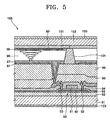
- FIG. 5 illustrates a liquid crystal display 105.
- a liquid crystal display and an electroluminescent display have a similar TFT panel structure, but different adjoining constitutional elements.
- adjoining constitutional elements of the TFT panel in a liquid crystal display will be described.
- a liquid crystal display 105 includes a TFT panel, a first orientation layer 97, a second substrate 102, a second electrode 62, a second orientation layer 99, a liquid crystal layer 98, and a polarization layer 103.
- the TFT panel includes a first substrate 91, a TFT 50, a first conductive line 20, a second conductive line 30, and a first electrode 61.
- the first substrate 91 corresponds to the substrate of an electroluminescent display.
- the first substrate 91 and the second substrate 102 are separately manufactured.
- a color filter layer 101 is formed on the lower surface of the second substrate 102.
- the second electrode 62 is formed on the lower surface of the color filter layer 101.
- the first orientation layer 97 and the second orientation layer 99 are formed on the upper surface of the first electrode 61 and the lower surface of the second electrode 62, respectively.
- the first and second orientation layers 97 and 99 lead to a proper orientation of a liquid crystal of the liquid crystal layer 98 interposed therebetween.
- the polarization layer 103 is formed on each of the outer surfaces of the first and second substrates 91 and 102 respectively.
- a spacer 104 is used to maintain a gap between the first and second substrates.
- a liquid crystal display allows light to pass through or be blocked according to the arrangement of a liquid crystal.
- the arrangement of the liquid crystal is determined by an electric potential difference between the first and second electrodes. Light that has passed through the liquid crystal layer exhibits a color of the color filter layer 101, thereby displaying an image.
- TFT conductive elements defined in the Description of the Related Art include the first and second source electrodes 12 and 52, the first and second drain electrodes 13 and 53, the first and second gate electrodes 11 and 51, the first conductive line 20, the second conductive line 30, and the third conductive line 70.
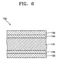
- the structures of the TFT conductive elements will be described in detail with reference to FIG. 6.
- the first and second gate electrodes 11 and 53 are formed simultaneously with the second conductive line 30 using the same material.
- the first and second source electrodes 12 .and 52, the first and second drain electrodes 13 and 53, the first conductive line 30, and the third conductive line 70 are at the same time formed using the same material. Since the formation sequences and materials for these TFT conductive elements may vary according to manufacture processes, they are not limited to those as described above.
- At least one of TFT conductive elements 130 according to the present invention includes an aluminum (Al)-based metal layer 131 and titanium (Ti) layers 132 and 133. Diffusion prevention layers 134 and 135 are interposed between the Al-based metal layer and the respective Ti layers.
- FIG. 6 illustrates that the diffusion prevention layers and the Ti layers are formed on both surfaces of the Al-based metal layer, a diffusion prevention layer and a Ti-layer may be formed on only one surface of the Al-based metal layer, that is also within the scope of the present invention.
- the second source electrode 52 and the second drain electrode 53 of FIG. 4 are formed in a vertically long shape.
- the layer structures of the second source electrode 52 and the second drain electrode 53 may be distorted. That is, although the second source electrode 52 and the second drain electrode 53 have a diffusion prevention layer and a Ti-layer between the Al-based metal layer 131 and the semiconductor layer 80, due to such distorted layer structure, the Al-based metal layer 131 and the semiconductor layer 80 may be partially in contact with each other. In this case, where the Al-based metal layer 131 is made of a pure Al, the Al can diffuse toward the semiconductor layer 80 made of silicon, thereby causing the malfunction of the semiconductor layer 80.
- the Al-based metal layer 131 is made of an Al alloy selected from the group consisting of an aluminum silicon (AlSi) alloy, an aluminum copper (AlCu) alloy, an aluminum neodymium (AINd) alloy, an aluminum platinum (AlPt) alloy, and an aluminum nickel (AINi) alloy.
- AlSi aluminum silicon
- AlCu aluminum copper
- AlPt aluminum neodymium
- AlPt aluminum platinum
- AINi aluminum nickel
- the Al-based metal layer 131 contains about 0.5 to 5 wt% of Si, Cu, Nd, Pt, or Ni. According to the results obtained from experiments, the AlSi alloy containing about 2 wt% of Si is more preferable.
- the Ti layers 132 and 133 serve to prevent the generation of Al hillocks during a heat treatment process.
- the diffusion prevention layers 134 and 135 serve to prevent the formation of TiAl 3 by reaction of the Al of the Al-based metal layer 131 with the Ti of the Ti layers 132 and 133 during the heat treatment process. By preventing the formation of TiAl 3 , the resistance of the TFT conductive elements 130 is reduced.
- the diffusion prevention layers 134 and 135 are made of TiN. This is because the TiN efficiently prevents the generation of TiAl 3 at an interface between the Al-based metal layer 131 and the Ti layers 132 and 133.
- the TiN layers134 and 135 contain 5 to 85 wt% of nitrogen.
- the Al-based metal layer 131 and the Ti layers 132 and 133 are deposited by DC-magnetron sputtering under an argon (Ar) gas atmosphere.
- the TiN layers 134 and 135 are deposited by reactive sputtering under a mixed gas atmosphere of Ar and nitrogen (N 2 ).
- Such a deposited structure is etched to a predetermined pattern for the TFT conductive elements 130 by dry etching with high frequency-enhanced plasma.
- the thickness of the TiN layers 134 and 135 are too thin, Al diffusion may occur. Therefore, the Al may easily react with the Ti of the Ti layers, thereby producing TiAl 3 .
- the TiN layers 134 and 135 are too thick, the resistance of the TFT conductive elements increases due to the high resistivity of the TiN.
- the TFT conductive elements 130 formed by interposing the TiN layers 134 and 135 between the Al-based metal layer 131 and the Ti layers 132 and 133 must have resistance lower than TFT conductive elements120 of FIG. 1. The thickness of the TiN layers satisfying these requirements is determined by following experiments and the results are presented in Table 1 below.
- Table 1 presents a change in resistivity according to the thickness of the TiN layers in TFT conductive elements having the structure of the Ti layer 132/the TiN layer 134/the Al-based metal layer 131/the TiN layer 135/the Ti layer 133 according to an embodiment of the present invention.
- each layer of the TFT conductive elements 130 is deposited by sputtering and then is subjected to heat treatment at 380°C in a vacuum to enhance the interface characteristics of the TFT conductive elements 130.
- Thickness of Ti layer 132 ( ⁇ ) Thickness of TiN layer 134 ( ⁇ ) Thickness of Al-based metal layer 131 ( ⁇ ) Thickness of TiN layer 135 ( ⁇ ) Thickness of Ti layer 133 ( ⁇ ) Total thickness ( ⁇ ) Resistivity ( ⁇ ⁇ cm) 500 0 4,000 0 500 5,000 17.24 500 100 3,800 100 500 5,000 5.34 500 200 3,600 200 500 5,000 4.51 500 300 3,400 300 500 5,000 4.23 500 400 3,200 400 500 5,000 4.62 500 500 3,000 500 500 5,000 5.02 500 600 2,800 600 500 5,000 5.36 500 700 2,600 700 500 5,000 5.68 500 800 2,400 800 500 5,000 6.47 500 900 2,200 900 500 5,000 7.03 500 1,000 2,000 1,000 500 5,000 7.78
- the graph of FIG. 7 is obtained from the results of Table 1.
- the line L represents ideal resistivity of TFT conductive elements of a thickness of 5,000 ⁇ made of Mo, i.e., theoretical minimal resistivity that is due to the resistivity of Mo. Using Mo, the ideal resistivity is 5.35 ⁇ ⁇ cm.
- a line M represents actual resistivity of TFT conductive elements 130 obtained empirically according to the present invention. That is, the resistivity of the line M is obtained by experiment.
- the thickness of the TiN layers 134 and 135 that result in a conductive element having a better resistivity than Mo based conductive elements satisfying the above-described requirements is a range of 100 to 600 ⁇
- the resistivity of the TFT conductive elements is relatively low when the TiN layers 134 and 135 have a thickness of 200 to 400 ⁇ .
- the resistivity of the TFT conductive elements is optimum when the TiN layers have a thickness of about 300 ⁇ .
- the TFT conductive elements having the TiN layers 134 and 135 with a thickness of 100 to 200 ⁇ and 400 to 600 ⁇ have resistivity lower than the TFT conductive elements made of only Mo, they have resistivity higher than the TFT conductive elements having the TiN layers 134 and 135 with a thickness of 200 to 400 ⁇ .
- the TiN layers 134 and 135 with a thickness of 100 to 200 ⁇ can be formed at a low cost, relative to the TiN layers 134 and 135 with a thickness of 400 to 600 ⁇ .
- FIG. 8 illustrates a resistance reduction effect of TFT conductive elements according to the present invention.
- the horizontal axis represents a temperature for a heat treatment process (heat treatment temperature) and the vertical axis represents resistivity of TFT conductive elements.
- the graph of A represents the resistivity of TFT conductive elements having a five layer structure of Ti layer (thickness: 500 ⁇ )/TiN layer (thickness: 500 ⁇ )/Al-based metal layer (thickness: 3,000 ⁇ )/TiN layer (thickness: 500 ⁇ )/Ti layer (thickness: 500 ⁇ ).
- the graph of B represents the resistivity of TFT conductive elements having a three layer structure of Ti layer (thickness: 500 ⁇ )/Al-based metal layer (thickness: 4,000 ⁇ )/Ti layer (thickness: 500 ⁇ ).
- the resistivity of the TFT conductive elements with the five layer structure is 5 ⁇ ⁇ cm
- the resistivity of the TFT conductive elements with the three layer structure is 21.5 ⁇ ⁇ cm, that is more than four times higher than the resistivity of the TFT conductive elements with the five layer structure.
- TFT conductive elements according to the present invention have the structure of Ti layer 132/TiN layer 134/Al-based metal layer 131/TiN layer 135/Ti layer 133.
- TFT conductive elements according to the present invention can have the structure of Ti layer 132/TiN layer 134/Al-based metal layer 131 because a resistance reduction effect is accomplished by the TiN layer interposed between the Al-based metal layer and the Ti layer.
- the present invention provides a TFT in that the generation of TiAl 3 is prevented and thus at least one of TFT conductive elements has a sufficiently low resistance, and a flat panel display including the TFT. Therefore, the flat panel display can have a fast response speed of sub-pixels and good image quality.
- the present invention also provides a TFT in that the generation of aluminum hillocks is prevented even after a heat treatment process, and a flat panel display including the TFT.
- the present invention also provides a TFT in that Al of TFT conductive elements does not diffuse toward a semiconductor layer, and a flat panel display including the TFT.
Landscapes
- Thin Film Transistor (AREA)
- Liquid Crystal (AREA)
- Electrodes Of Semiconductors (AREA)
- Electroluminescent Light Sources (AREA)
- Devices For Indicating Variable Information By Combining Individual Elements (AREA)
- Physical Vapour Deposition (AREA)
Abstract
Description
- The present invention relates to thin film transistors in a flat panel display. More particularly, the present invention relates to a novel structure for the electrodes and conductive lines found in thin film transistor structures that have small resistance loss and prevent image quality degradation caused by resistance loss in a large flat panel display.
- A thin film transistor (hereinafter, referred to as TFT) is a device in which a source electrode and a drain electrode can be electrically connected through a channel formed in a semiconductor layer that physically connects the source and drain electrodes according to a voltage applied to a gate electrode. The TFT is mainly used in a TFT panel of an active matrix flat panel display such as an electroluminescent display and a liquid crystal display. The TFT serves to independently drive sub-pixels that make up the display.
- A source electrode and a gate electrode of a TFT formed in a flat panel display are connected to driving circuits arranged on sides of the flat panel display through conductive lines. Generally, a source electrode, a drain electrode, and conductive lines electrically connected to the source and drain electrodes are often formed together and have the same structure using the same material for the sake of simplifying a manufacture process.
- A source electrode, a drain electrode, and conductive lines electrically connected thereto may be made of a chromium (Cr) based metal or a molybdenum (Mo) based metal such as Mo and MoW. However, since these metals have a relatively high resistance, in a case where a TFT panel has a large size or its sub-pixels have small sizes, a voltage drop between driving circuits and the sub-pixels may increase. This causes a response speed of the sub-pixels to decrease or to result in a non-uniform distribution of an image. These problems of speed and non-uniformity of image are further aggravated by the fact that newer displays are large, and the conductive lines that electrically connect to the pixels in aq large display are very long. These long conductive lines found in large displays magnify the resistive losses in a conductive line. Therefore, in recent years, with the advent of large TFT displays, it is even more important to use materials with low resistive losses to electrically connect to each TFT in a display.
- In addition to the fact that newer displays are large, the speed and non-uniformity problem are further aggravated by the fact that these conductive lines generally undergo a heat treatment process subsequent to formation of these conductive lines and electrodes. For example, the activation process after gate metal sputtering is necessary in TFT fabrication, and the temperature of annealing is generally needed to be higher than 400°C . In this case, the high temperature annealing may cause connection lines and electrodes to form at a high resistance, especially when incorporated in a large display panel.
- In order to solve the above problems, aluminum (Al) has been used in conductive lines and electrode structures for TFT's. Aluminum may have a low resistance as a material for a gate electrode and a conductive line connecting the gate electrode to a driving circuit. Aluminum may also drop the resistance in source electrodes, drain electrodes, and conductive lines electrically connected to the source and drain electrodes. Hereinafter, the source electrode, the drain electrode, the gate electrode and the conductive lines electrically connected to the source, drain and gate electrodes will be referred to as "TFT conductive elements."
- U.S. Patent Application Laid-Open Publication No. 2002/0085157 to Tanaka et al (hereinafter Tanaka '157) discloses TFT conductive elements made of Al. Each of the TFT conductive elements has a stacked structure of titanium nitride (TiN) layer/Al layer, TiN layer/Ti layer/Al layer, or TiN layer/Al layer/Ti layer, as illustrated in FIG. 7 of Tanaka '157. Advantages of such a structure include reduction of an electrical connection resistance (or contact resistance) between the TFT conductive elements and terminals connected to the TFT conductive elements as well as suppression of the generation of Al hillocks (or small hills or mounds) generated by a heat treatment process subsequent to the formation of the TFT conductive elements. However, Tanaka '157 fails to disclose solutions to reduce the resistance of the TFT conductive elements. Tanaka '157 fails to address prevention of the formation of highly resistive TiAl3 when heat treated. TiAl3 in the conductive layers causes the resistance of the conductive lines to increase, especially for large displays.
- What is therefore needed is a structure for conductive lines as well as structures for electrodes in TFT's for a large display that have a low resistance, even after a heat treatment, the conductive lines and electrodes do not have TiAl3 present and have no hillocks even after heat treatment.
- According to an aspect of the invention, there is provided a thin film transistor comprising a source electrode, a drain electrode, a gate electrode, and a semiconductor layer, where at least one of the source electrode, the drain electrode, and the gate electrode comprises an aluminum-based metal layer, a titanium layer, and a diffusion prevention layer interposed the aluminum-based metal layer and the titanium layer.
- According to another aspect of the present invention, there is provided a large flat panel display having a large number of sub-pixels driven by TFTs, each of the TFTs having the features described above.
- The diffusion prevention layer prevents aluminum in the aluminum-based layer from reacting with the titanium in the titanium layer during the heat treatment or annealing process and forming unwanted TiAl3, the presence of which increases the resistance or resistivity of the connection members.
- The diffusion prevention layer and the titanium layer may be orderly formed on opposite surfaces of the aluminum-based metal layer, or the diffusion prevention layer and the titanium layer may be formed on any one side of the aluminum-based metal layer. The diffusion prevention layer may be a titanium nitride layer. The titanium nitride layer may contain 5 to 85 wt% of nitrogen. The titanium nitride layer may have a thickness of about 100 to 600Å, preferably about 100 to 400Å, more preferably 200 to 400Å, and most preferably about 300Å.
- The aluminum-based metal layer may be made of an aluminum alloy containing about 0.5 to 5 wt% of one element selected from the group consisting of silicon, copper, neodymium, platinum, and nickel. The aluminum-based metal layer may be made of an aluminum-silicon alloy containing about 2 wt% of silicon.
- The present invention thus provides a novel structure for conductive elements used in a TFT in a flat panel display that has a low resistivity, even after a heat treatment.
- The present invention also provides a novel structure for a conductive layer for conductive elements in a TFT in a display that is made using aluminum and does not have any hillocks and does not have any TiAl3, even after a heat treatment.
- The present invention also provides a novel structure for conductive lines and electrodes used in TFT displays that improves display uniformity and improves speed, especially when the display is very large.
- A more complete appreciation of the invention, and many of the attendant advantages thereof, will be readily apparent as the same becomes better understood by reference to the following detailed description when considered in conjunction with the accompanying drawings in which like reference symbols indicate the same or similar components, wherein:
- FIG. 1 is a sectional view of a TFT conductive element;
- FIG. 2 is a circuit view of a flat panel display having an array of TFTs;
- FIG. 3 is a schematic plan view of the physical structure of one sub-pixel corresponding to a part "S" of FIG. 2;
- FIG. 4 is a sectional view of one sub-pixel of an electroluminescent display having a TFT;
- FIG. 5 is a sectional view of one sub-pixel of a liquid crystal display having a TFT;
- FIG. 6 is a sectional view of a TFT conductive element according to the principles of the present invention;
- FIG. 7 is a graph illustrating empirical resistivity versus thickness of a titanium nitride layer in the novel TFT conductive element according to the present invention; and
- FIG. 8 is a graph illustrating empirically resistivity versus heat treatment temperature in a TFT conductive element and a TFT conductive element according to the principles of the present invention.
-
- Turning now to the Figures, FIG. 1 illustrates a TFT
conductive element 120 having a stacked structure of aTi layer 122, anAl layer 121, and aTi layer 123. The Ti layers prevent the generation of Al hillocks formed during a heat treatment process. However, TiAl3 may be generated at an interface between the Al layer and the Ti layer during a heat treatment process. The TiAl3 increases the resistance of the TFT conductive element. - FIG. 2 illustrates a
circuit 112 of a flat panel display made up many sub-pixels, each sub-pixel having two TFT's. Thecircuit 112 includes afirst TFT 10, asecond TFT 50, astorage capacitor 40, and alight emission unit 60. Afirst source electrode 12 in thefirst TFT 10 is connected to a horizontal driving circuit H through a firstconductive line 20 and afirst gate electrode 11 in the first TFT 10 is connected to a vertical driving circuit V through a secondconductive line 30. Afirst drain electrode 13 in thefirst TFT 10 is connected to afirst capacitor electrode 41 of thestorage capacitor 40 and to asecond gate electrode 51 of thesecond TFT 50. Asecond capacitor electrode 42 of thestorage capacitor 40 and asecond source electrode 52 of thesecond TFT 50 are connected to a thirdconductive line 70. Asecond drain electrode 53 of the second TFT is connected to afirst electrode 61 of thelight emission unit 60. Asecond electrode 62 of thelight emission unit 60 is arranged opposite to thefirst electrode 61 and spaced a predetermined gap apart from thefirst electrode 61. Betweensecond electrode 62 andfirst electrode 61 is an active layer. The active layer may be an organic material layer, an inorganic material layer, or a liquid crystal layer and is arranged between thefirst electrode 61 andsecond electrode 62 according to the types of flat panel displays. - FIG. 3 schematically illustrates a physical structure of one sub-pixel of the flat panel display of FIG. 2. For the sake of simplicity, only conductive constitutional elements are illustrates in FIG. 3. Therefore, nonconductive constitutional elements such as a substrate, a buffer layer, various types of insulating layers, a planarization layer, a light emission layer, a liquid crystal layer, a second electrode, a polarization layer, an orientation layer, and a color filter layer are omitted. These nonconductive constitutional elements are instead illustrated in FIGS. 4 and 5. Only constitutional elements positioned at regions represented by oblique (or slanted) lines in FIG. 3 are electrically connected to each other. Other regions that are not represented by oblique lines are insulated.
- When a voltage is applied to the
first gate electrode 11, a conductive channel is formed in asemiconductor layer 80 that connects thefirst source electrode 12 and thefirst drain electrode 13. At this time, when charge is supplied to thefirst source electrode 12 through the firstconductive line 20, the charge moves into thefirst drain electrode 13. Charge determining the luminance of a driving unit flows through the thirdconductive line 70. When the charge of the first drain electrode is supplied to thesecond gate electrode 51, the charge of thesecond source electrode 52 moves into thesecond drain electrode 53, thereby driving thefirst electrode 61 of thelight emission unit 60. Thestorage capacitor 40 serves to maintain a driving operation of thefirst electrode 61 or increase a driving speed. For reference, thefirst TFT 10 and thesecond TFT 50 have a similar section structure. - An
electroluminescent display 114 illustrated in FIG. 4 includes a TFT panel, alight emission layer 87, and asecond electrode 62. The TFT panel includes asubstrate 81, aTFT 50, a firstconductive line 20, a secondconductive line 30, and afirst electrode 61. In the case of a rear emission type electroluminescent display, thesubstrate 81 may be made of a transparent material, for example glass, and thesecond electrode 62 may be made of a metal with good reflectivity such as aluminium. On the other hand, in the case of a front emission type electroluminescent display, thesecond electrode 62 may be made of a transparent conductive material, for example, indium tin oxide (ITO), and thefirst electrode 61 may be made of a metal with good reflectivity. - A
buffer layer 82 is formed on the whole surface of thesubstrate 81. Asemiconductor layer 80 is formed to a predetermined pattern on thebuffer layer 82.Semiconductor layer 80 may be made of silicon. A first insulatinglayer 83 is formed on thesemiconductor layer 80 and on the remaining exposed surface of thebuffer layer 82 where thesemiconductor layer 80 is not formed. Asecond gate electrode 51 is formed to a predetermined pattern on the first insulatinglayer 83. A second insulatinglayer 84 is formed on thesecond gate electrode 51 and on the remaining exposed surface of the first insulatinglayer 83 on where thesecond gate electrode 51 is not formed. After the formation of the second insulatinglayer 84, the first and second insulatinglayers semiconductor layer 80. The exposed portions of thesemiconductor layer 80 are connected to asecond source electrode 52 and asecond drain electrode 53, that are formed to a predetermined pattern. After the formation of the second source and drainelectrodes layer 85 is formed thereon. A portion of the third insulatinglayer 85 is etched to electrically connect thesecond drain electrode 53 and thefirst electrode 61. After the formation of thefirst electrode 61 on the third insulatinglayer 85, aplanarization layer 86 is formed. The portion of theplanarization layer 86 corresponding to thefirst electrode 61 is etched. Then, thelight emission layer 87 is formed on thefirst electrode 61 and thesecond electrode 62 is formed on thelight emission layer 87. - The
TFT 50 includes thesecond source electrode 52, thesecond drain electrode 53, thesecond gate electrode 51, and thesemiconductor layer 80. Generally, thesecond source electrode 52 and thesecond drain electrode 53 are formed at a predetermined gap from each other on the same horizontal plane. Thesecond source electrode 52 and thesecond drain electrode 53 are physically connected to thesemiconductor layer 80. Thesecond gate electrode 51 is electrically insulated from thesecond source electrode 52, thesecond drain electrode 53, and thesemiconductor layer 80. Thesecond gate electrode 51 is positioned above thesemiconductor layer 80 and between thesecond source electrode 52 and thesecond drain electrode 53. Meanwhile, generally, a TFT is divided into a staggered type, an inverted staggered type, a coplanar type, and an inverted coplanar type according to the arrangements of the above electrodes and thesemiconductor layer 80. A coplanar type is illustrated in the present invention, but the present invention is not limited thereto. - The
TFT 50 of FIG. 4 corresponds to thesecond TFT 50 illustrated in FIG. 3. In this case, thesecond source electrode 52 is connected to the thirdconductive line 70, thesecond gate electrode 51 is connected to thefirst drain electrode 13 of thefirst TFT 10, thesecond drain electrode 53 is connected to thefirst electrode 61 oflight emitting unit 60, thefirst source electrode 12 of thefirst TFT 10 is connected to the firstconductive line 20, and thefirst gate electrode 11 is connected to the secondconductive line 30. According to the present invention, the firstconductive line 20 corresponds to a data line for transmitting data and the secondconductive line 30 corresponds to a scan line. - The structure of an
electroluminescent display 114 will now be described in detail with reference to FIG. 4. As illustrated in FIG. 4, anelectroluminescent display 114 includes thefirst electrode 61, thelight emission layer 87 formed on thefirst electrode 61, and thesecond electrode 62 formed on thelight emission layer 87. Anelectroluminescent display 114 can be divided into organic and inorganic electroluminescent displays. With respect to an organic electroluminescent display, thelight emission layer 87 is largely having an electron transport layer, a light emission material layer, and a hole transport layer. With respect to an inorganic electroluminescent display, insulating layers are interposed between thefirst electrode 61 and thelight emission layer 87 and between thesecond electrode 62 and thelight emission layer 87. - The
light emission layer 87 of an organic electroluminescent display is made of an organic material, for example, phthalocyanine such as copper phthalocyanine (CuPc), N,N'-di(naphthalene-1-yl)-N,N'-diphenyl benzidine (NPB), or tris-8-hydroxyquinoline aluminium (Alq3). When charge is supplied to thefirst electrode 61 and thesecond electrode 62, holes and electrons recombine with each other to generate excitons. When the excitons are changed from an excited state to a ground state, the lightemission material layer 87 emits light. - Regarding an inorganic electroluminescent display, an inorganic material layer between the insulating layers positioned at inner sides of the
first electrode 61 andsecond electrode 62 emits light. An inorganic material for the inorganic material layer may be metal sulfide such as ZnS, SrS, and CsS. Recently, alkaline earth-based calcium sulfide such as CaCa2S4 and SrCa2S4, and metal oxide are also used. Transition metals such as Mn, Ce, Tb, Eu, Tm, Er, Pr, and Pb and alkaline rare earth metals may be used as light emitting core atoms that form thelight emission layer 87 together with the above inorganic material. When a voltage is applied to thefirst electrode 61 andsecond electrode 62, electrons are accelerated and collide with the light emitting core atoms. At this time, electrons of the light emitting core atoms are excited to a higher energy level and then fall back to a ground state. Accordingly, the inorganic material layer emits light. - FIG. 5 illustrates a
liquid crystal display 105. A liquid crystal display and an electroluminescent display have a similar TFT panel structure, but different adjoining constitutional elements. Hereinafter, only adjoining constitutional elements of the TFT panel in a liquid crystal display will be described. - A
liquid crystal display 105 includes a TFT panel, afirst orientation layer 97, asecond substrate 102, asecond electrode 62, asecond orientation layer 99, aliquid crystal layer 98, and apolarization layer 103. The TFT panel includes afirst substrate 91, aTFT 50, a firstconductive line 20, a secondconductive line 30, and afirst electrode 61. Thefirst substrate 91 corresponds to the substrate of an electroluminescent display. - The
first substrate 91 and thesecond substrate 102 are separately manufactured. Acolor filter layer 101 is formed on the lower surface of thesecond substrate 102. Thesecond electrode 62 is formed on the lower surface of thecolor filter layer 101. Thefirst orientation layer 97 and thesecond orientation layer 99 are formed on the upper surface of thefirst electrode 61 and the lower surface of thesecond electrode 62, respectively. The first and second orientation layers 97 and 99 lead to a proper orientation of a liquid crystal of theliquid crystal layer 98 interposed therebetween. Thepolarization layer 103 is formed on each of the outer surfaces of the first andsecond substrates spacer 104 is used to maintain a gap between the first and second substrates. - A liquid crystal display allows light to pass through or be blocked according to the arrangement of a liquid crystal. The arrangement of the liquid crystal is determined by an electric potential difference between the first and second electrodes. Light that has passed through the liquid crystal layer exhibits a color of the
color filter layer 101, thereby displaying an image. - According to the present invention, "TFT conductive elements" defined in the Description of the Related Art include the first and
second source electrodes second drain electrodes second gate electrodes conductive line 20, the secondconductive line 30, and the thirdconductive line 70. Hereinafter, the structures of the TFT conductive elements will be described in detail with reference to FIG. 6. - According to the present invention, the first and
second gate electrodes conductive line 30 using the same material. The first andsecond source electrodes 12 .and 52, the first andsecond drain electrodes conductive line 30, and the thirdconductive line 70 are at the same time formed using the same material. Since the formation sequences and materials for these TFT conductive elements may vary according to manufacture processes, they are not limited to those as described above. - At least one of TFT
conductive elements 130 according to the present invention includes an aluminum (Al)-basedmetal layer 131 and titanium (Ti) layers 132 and 133. Diffusion prevention layers 134 and 135 are interposed between the Al-based metal layer and the respective Ti layers. Although FIG. 6 illustrates that the diffusion prevention layers and the Ti layers are formed on both surfaces of the Al-based metal layer, a diffusion prevention layer and a Ti-layer may be formed on only one surface of the Al-based metal layer, that is also within the scope of the present invention. - Among the TFT conductive elements, in particular, the
second source electrode 52 and thesecond drain electrode 53 of FIG. 4 are formed in a vertically long shape. For this reason, the layer structures of thesecond source electrode 52 and thesecond drain electrode 53 may be distorted. That is, although thesecond source electrode 52 and thesecond drain electrode 53 have a diffusion prevention layer and a Ti-layer between the Al-basedmetal layer 131 and thesemiconductor layer 80, due to such distorted layer structure, the Al-basedmetal layer 131 and thesemiconductor layer 80 may be partially in contact with each other. In this case, where the Al-basedmetal layer 131 is made of a pure Al, the Al can diffuse toward thesemiconductor layer 80 made of silicon, thereby causing the malfunction of thesemiconductor layer 80. In this regard, it is preferable to form the Al-basedmetal layer 131 using a material that does not easily diffuse toward thesemiconductor layer 80 even though the Al-basedmetal layer 131 is in contact with thesemiconductor layer 80. Therefore, preferably, the Al-basedmetal layer 131 is made of an Al alloy selected from the group consisting of an aluminum silicon (AlSi) alloy, an aluminum copper (AlCu) alloy, an aluminum neodymium (AINd) alloy, an aluminum platinum (AlPt) alloy, and an aluminum nickel (AINi) alloy. Si, Cu, Nd, Pt, and Ni contained in the Al alloys serve to prevent the diffusion of Al of the Al-based metal layer toward thesemiconductor layer 80 made of Si. Preferably, the Al-basedmetal layer 131 contains about 0.5 to 5 wt% of Si, Cu, Nd, Pt, or Ni. According to the results obtained from experiments, the AlSi alloy containing about 2 wt% of Si is more preferable. - The Ti layers 132 and 133 serve to prevent the generation of Al hillocks during a heat treatment process. The diffusion prevention layers 134 and 135 serve to prevent the formation of TiAl3 by reaction of the Al of the Al-based
metal layer 131 with the Ti of the Ti layers 132 and 133 during the heat treatment process. By preventing the formation of TiAl3, the resistance of the TFTconductive elements 130 is reduced. Preferably, the diffusion prevention layers 134 and 135 are made of TiN. This is because the TiN efficiently prevents the generation of TiAl3 at an interface between the Al-basedmetal layer 131 and the Ti layers 132 and 133. Preferably, the TiN layers134 and 135 contain 5 to 85 wt% of nitrogen. - For reference, the Al-based
metal layer 131 and the Ti layers 132 and 133 are deposited by DC-magnetron sputtering under an argon (Ar) gas atmosphere. The TiN layers 134 and 135 are deposited by reactive sputtering under a mixed gas atmosphere of Ar and nitrogen (N2). Such a deposited structure is etched to a predetermined pattern for the TFTconductive elements 130 by dry etching with high frequency-enhanced plasma. - If the thickness of the TiN layers 134 and 135 are too thin, Al diffusion may occur. Therefore, the Al may easily react with the Ti of the Ti layers, thereby producing TiAl3. On the other hand, the TiN layers 134 and 135 are too thick, the resistance of the TFT conductive elements increases due to the high resistivity of the TiN. The TFT
conductive elements 130 formed by interposing the TiN layers 134 and 135 between the Al-basedmetal layer 131 and the Ti layers 132 and 133 must have resistance lower than TFT conductive elements120 of FIG. 1. The thickness of the TiN layers satisfying these requirements is determined by following experiments and the results are presented in Table 1 below. - Table 1 presents a change in resistivity according to the thickness of the TiN layers in TFT conductive elements having the structure of the
Ti layer 132/theTiN layer 134/the Al-basedmetal layer 131/theTiN layer 135/theTi layer 133 according to an embodiment of the present invention. For this, each layer of the TFTconductive elements 130 is deposited by sputtering and then is subjected to heat treatment at 380°C in a vacuum to enhance the interface characteristics of the TFTconductive elements 130.Thickness of Ti layer 132 (Å) Thickness of TiN layer 134 (Å) Thickness of Al-based metal layer 131 (Å) Thickness of TiN layer 135 (Å) Thickness of Ti layer 133 (Å) Total thickness (Å) Resistivity (µ Ωcm) 500 0 4,000 0 500 5,000 17.24 500 100 3,800 100 500 5,000 5.34 500 200 3,600 200 500 5,000 4.51 500 300 3,400 300 500 5,000 4.23 500 400 3,200 400 500 5,000 4.62 500 500 3,000 500 500 5,000 5.02 500 600 2,800 600 500 5,000 5.36 500 700 2,600 700 500 5,000 5.68 500 800 2,400 800 500 5,000 6.47 500 900 2,200 900 500 5,000 7.03 500 1,000 2,000 1,000 500 5,000 7.78 - The graph of FIG. 7 is obtained from the results of Table 1. In FIG. 7, the line L represents ideal resistivity of TFT conductive elements of a thickness of 5,000Å made of Mo, i.e., theoretical minimal resistivity that is due to the resistivity of Mo. Using Mo, the ideal resistivity is 5.35 µ Ωcm. In FIG. 7, a line M represents actual resistivity of TFT
conductive elements 130 obtained empirically according to the present invention. That is, the resistivity of the line M is obtained by experiment. - From the graph M of FIG. 7, it can be seen that the thickness of the TiN layers 134 and 135 that result in a conductive element having a better resistivity than Mo based conductive elements satisfying the above-described requirements is a range of 100 to 600Å The resistivity of the TFT conductive elements is relatively low when the TiN layers 134 and 135 have a thickness of 200 to 400Å. In particular, the resistivity of the TFT conductive elements is optimum when the TiN layers have a thickness of about 300Å. While the TFT conductive elements having the TiN layers 134 and 135 with a thickness of 100 to 200Å and 400 to 600Å have resistivity lower than the TFT conductive elements made of only Mo, they have resistivity higher than the TFT conductive elements having the TiN layers 134 and 135 with a thickness of 200 to 400Å. The TiN layers 134 and 135 with a thickness of 100 to 200Å can be formed at a low cost, relative to the TiN layers 134 and 135 with a thickness of 400 to 600Å.
- FIG. 8 illustrates a resistance reduction effect of TFT conductive elements according to the present invention. In FIG. 8, the horizontal axis represents a temperature for a heat treatment process (heat treatment temperature) and the vertical axis represents resistivity of TFT conductive elements. The graph of A represents the resistivity of TFT conductive elements having a five layer structure of Ti layer (thickness: 500Å)/TiN layer (thickness: 500Å)/Al-based metal layer (thickness: 3,000Å)/TiN layer (thickness: 500Å)/Ti layer (thickness: 500Å). The graph of B represents the resistivity of TFT conductive elements having a three layer structure of Ti layer (thickness: 500Å)/Al-based metal layer (thickness: 4,000Å)/Ti layer (thickness: 500Å). As illustrated in FIG. 8, for example, at a heat treatment temperature of 380°C, while the resistivity of the TFT conductive elements with the five layer structure is 5 µ Ωcm, the resistivity of the TFT conductive elements with the three layer structure is 21.5 µ Ωcm, that is more than four times higher than the resistivity of the TFT conductive elements with the five layer structure.
- In the above case, it is illustrated that TFT conductive elements according to the present invention have the structure of
Ti layer 132/TiN layer 134/Al-basedmetal layer 131/TiN layer 135/Ti layer 133. However, it is understood that TFT conductive elements according to the present invention can have the structure ofTi layer 132/TiN layer 134/Al-basedmetal layer 131 because a resistance reduction effect is accomplished by the TiN layer interposed between the Al-based metal layer and the Ti layer. - As is apparent from the above description, the present invention provides a TFT in that the generation of TiAl3 is prevented and thus at least one of TFT conductive elements has a sufficiently low resistance, and a flat panel display including the TFT. Therefore, the flat panel display can have a fast response speed of sub-pixels and good image quality. The present invention also provides a TFT in that the generation of aluminum hillocks is prevented even after a heat treatment process, and a flat panel display including the TFT. The present invention also provides a TFT in that Al of TFT conductive elements does not diffuse toward a semiconductor layer, and a flat panel display including the TFT.
- While the present invention has been particularly illustrated and described with reference to exemplary embodiments thereof, it will be understood by those of ordinary skill in the art that various changes in form and details may be made therein without departing from the scope of the present invention as defined by the following claims.
Claims (17)
- A thin film transistor, comprising a source electrode, a drain electrode, a gate electrode, and a semiconductor layer, wherein at least one of the source electrode, the drain electrode, and the gate electrode comprises an aluminum-based metal layer, a titanium layer, and a diffusion prevention layer interposed between the aluminum-based metal layer and the titanium layer.
- The thin film transistor of claim 1, wherein the diffusion prevention layer and the titanium layer are both orderly formed on opposite surfaces of the aluminum-based metal layer.
- The thin film transistor of claim 1 or 2, wherein the diffusion prevention layer is a titanium nitride layer.
- The thin film transistor of claim 3, wherein the titanium nitride layer contains 5 to 85 wt% of nitrogen.
- The thin film transistor of claim 3 or 4, wherein the titanium nitride layer has a thickness of about 100 to 600Å.
- The thin film transistor of any one of claims 3 to 5, wherein the titanium nitride layer has a thickness of about 100 to 400Å.
- The thin film transistor of any one of claims 3 to 6, wherein the titanium nitride layer has a thickness of 200 to 400Å.
- The thin film transistor of any one of claims 3 to 7, wherein the titanium nitride layer has a thickness of about 300Å.
- The thin film transistor of any one of the preceding claims, wherein the aluminum-based metal layer is made of an aluminum alloy containing about 0.5 to 5 wt% of one element being selected from the group consisting of silicon, copper, neodymium, platinum, and nickel.
- The thin film transistor of claim 9, wherein the aluminum-based metal layer is made of an aluminum-silicon alloy containing about 2 wt% of silicon.
- A flat panel display, comprising a plurality of sub-pixels driven by thin film transistors according to any one of the preceding claims.
- A flat panel display, comprising:driving circuits disposed along edges of said display;a plurality of sub-pixels driven by thin film transistors; andconductive lines connecting the driving circuits disposed along edges of said display to each of said plurality of sub-pixels, wherein said conductive lines comprise an aluminum-based metal layer, a titanium layer, and a diffusion prevention layer interposed between the aluminum-based metal layer and the titanium layer.
- The flat panel display of claim 12, wherein the diffusion prevention layer and the titanium layer are both orderly formed on opposite sides of the aluminum-based metal layer.
- The flat panel display of claim 12 or 13, wherein the diffusion prevention layer is a titanium nitride layer.
- The display of claim 14, said titanium nitride layer is 300 Å thick.
- The display of any one of claims 12 to 15, wherein said conductive lines have been subjected to a heat treatment of 380°C.
- A conductive element comprising:an aluminum-based metal layer;a titanium layer; anda diffusion prevention layer interposed between the titanium layer and the aluminum-based metal layer.
Applications Claiming Priority (4)
| Application Number | Priority Date | Filing Date | Title |
|---|---|---|---|
| KR2003015356 | 2003-03-12 | ||
| KR20030015356 | 2003-03-12 | ||
| KR2003063583 | 2003-09-15 | ||
| KR1020030063583A KR100553747B1 (en) | 2003-03-12 | 2003-09-15 | Thin film transistor and flat display device comprising it |
Publications (2)
| Publication Number | Publication Date |
|---|---|
| EP1458029A2 true EP1458029A2 (en) | 2004-09-15 |
| EP1458029A3 EP1458029A3 (en) | 2006-03-15 |
Family
ID=32775313
Family Applications (1)
| Application Number | Title | Priority Date | Filing Date |
|---|---|---|---|
| EP04250453A Ceased EP1458029A3 (en) | 2003-03-12 | 2004-01-28 | Novel conductive elements for thin film transistors used in a flat panel display |
Country Status (4)
| Country | Link |
|---|---|
| US (2) | US7317206B2 (en) |
| EP (1) | EP1458029A3 (en) |
| JP (1) | JP4038485B2 (en) |
| CN (1) | CN100419550C (en) |
Families Citing this family (16)
| Publication number | Priority date | Publication date | Assignee | Title |
|---|---|---|---|---|
| JP4038485B2 (en) * | 2003-03-12 | 2008-01-23 | 三星エスディアイ株式会社 | Flat panel display device with thin film transistor |
| US7791072B2 (en) * | 2004-11-10 | 2010-09-07 | Canon Kabushiki Kaisha | Display |
| JP4650224B2 (en) * | 2004-11-19 | 2011-03-16 | 日亜化学工業株式会社 | Field effect transistor |
| US7683370B2 (en) | 2005-08-17 | 2010-03-23 | Kobe Steel, Ltd. | Source/drain electrodes, transistor substrates and manufacture methods, thereof, and display devices |
| KR100774950B1 (en) * | 2006-01-19 | 2007-11-09 | 엘지전자 주식회사 | Electroluminescent element |
| US7781767B2 (en) * | 2006-05-31 | 2010-08-24 | Kobe Steel, Ltd. | Thin film transistor substrate and display device |
| US9419181B2 (en) | 2013-05-13 | 2016-08-16 | Infineon Technologies Dresden Gmbh | Electrode, an electronic device, and a method for manufacturing an optoelectronic device |
| CN103779358A (en) | 2014-01-27 | 2014-05-07 | 京东方科技集团股份有限公司 | Array substrate, manufacturing method of array substrate and display device |
| US9548349B2 (en) | 2014-06-25 | 2017-01-17 | International Business Machines Corporation | Semiconductor device with metal extrusion formation |
| US9711350B2 (en) | 2015-06-03 | 2017-07-18 | Asm Ip Holding B.V. | Methods for semiconductor passivation by nitridation |
| CN105140199B (en) * | 2015-08-11 | 2018-06-29 | 上海华虹宏力半导体制造有限公司 | Top-level metallic membrane structure and aluminum manufacturing procedure process |
| KR20190043194A (en) * | 2017-10-17 | 2019-04-26 | 삼성디스플레이 주식회사 | Metal line and thin film transistor |
| KR102554830B1 (en) * | 2018-10-04 | 2023-07-13 | 삼성디스플레이 주식회사 | Display apparatus and method of manufacturing the same |
| KR102839408B1 (en) | 2019-01-17 | 2025-07-28 | 삼성디스플레이 주식회사 | Display devices and manufacturing method thereof |
| KR102819170B1 (en) * | 2019-02-18 | 2025-06-12 | 삼성디스플레이 주식회사 | Display device and method of manufacturing the display device |
| CN113629078A (en) * | 2021-08-23 | 2021-11-09 | 京东方科技集团股份有限公司 | Conductive structure layer, display panel and manufacturing method thereof |
Citations (3)
| Publication number | Priority date | Publication date | Assignee | Title |
|---|---|---|---|---|
| US5427666A (en) * | 1993-09-09 | 1995-06-27 | Applied Materials, Inc. | Method for in-situ cleaning a Ti target in a Ti + TiN coating process |
| JP2003015105A (en) * | 2001-06-28 | 2003-01-15 | Hitachi Ltd | Image display device |
| EP1458030A2 (en) * | 2003-03-12 | 2004-09-15 | Samsung SDI Co., Ltd. | Novel and conductive elements for thin film transistors used in a flat panel display |
Family Cites Families (71)
| Publication number | Priority date | Publication date | Assignee | Title |
|---|---|---|---|---|
| US555112A (en) * | 1896-02-25 | August j | ||
| US4153529A (en) | 1975-04-21 | 1979-05-08 | Hughes Aircraft Company | Means and method for inducing uniform parallel alignment of liquid crystal material in a liquid crystal cell |
| DE8232492U1 (en) | 1982-11-19 | 1986-03-27 | Siemens AG, 1000 Berlin und 8000 München | Amorphous silicon solar cell |
| JPS59232464A (en) | 1983-06-16 | 1984-12-27 | Hitachi Ltd | compound semiconductor device |
| US5278099A (en) | 1985-05-13 | 1994-01-11 | Kabushiki Kaisha Toshiba | Method for manufacturing a semiconductor device having wiring electrodes |
| US4646424A (en) | 1985-08-02 | 1987-03-03 | General Electric Company | Deposition and hardening of titanium gate electrode material for use in inverted thin film field effect transistors |
| US4933296A (en) | 1985-08-02 | 1990-06-12 | General Electric Company | N+ amorphous silicon thin film transistors for matrix addressed liquid crystal displays |
| JPS62120076A (en) | 1985-11-20 | 1987-06-01 | Fujitsu Ltd | Thin film transistor |
| JPS62221159A (en) | 1986-03-24 | 1987-09-29 | Fujitsu Ltd | Formation of thin film transistor matrix |
| US4782380A (en) | 1987-01-22 | 1988-11-01 | Advanced Micro Devices, Inc. | Multilayer interconnection for integrated circuit structure having two or more conductive metal layers |
| JPS6419763U (en) | 1987-07-24 | 1989-01-31 | ||
| US4910580A (en) | 1987-08-27 | 1990-03-20 | Siemens Aktiengesellschaft | Method for manufacturing a low-impedance, planar metallization composed of aluminum or of an aluminum alloy |
| JPH0351016Y2 (en) | 1987-08-28 | 1991-10-31 | ||
| US4778258A (en) | 1987-10-05 | 1988-10-18 | General Electric Company | Protective tab structure for use in the fabrication of matrix addressed thin film transistor liquid crystal displays |
| JPH0666287B2 (en) | 1988-07-25 | 1994-08-24 | 富士通株式会社 | Method for manufacturing semiconductor device |
| US5243202A (en) | 1990-04-25 | 1993-09-07 | Casio Computer Co., Ltd. | Thin-film transistor and a liquid crystal matrix display device using thin-film transistors of this type |
| JPH04265757A (en) | 1991-02-21 | 1992-09-21 | Matsushita Electric Ind Co Ltd | Thin film thermal head |
| US5345108A (en) | 1991-02-26 | 1994-09-06 | Nec Corporation | Semiconductor device having multi-layer electrode wiring |
| JP2533414B2 (en) | 1991-04-09 | 1996-09-11 | 三菱電機株式会社 | Wiring connection structure of semiconductor integrated circuit device and manufacturing method thereof |
| US5485019A (en) | 1992-02-05 | 1996-01-16 | Semiconductor Energy Laboratory Co., Ltd. | Semiconductor device and method for forming the same |
| KR950009934B1 (en) | 1992-09-07 | 1995-09-01 | 삼성전자주식회사 | Metalizing method of semiconductor device |
| JP3587537B2 (en) | 1992-12-09 | 2004-11-10 | 株式会社半導体エネルギー研究所 | Semiconductor device |
| JPH06250211A (en) | 1993-02-23 | 1994-09-09 | Hitachi Ltd | Liquid crystal display substrate and its production |
| JP3613768B2 (en) | 1993-08-11 | 2005-01-26 | ヤマハ株式会社 | Semiconductor device |
| JPH07120789A (en) | 1993-10-28 | 1995-05-12 | Hitachi Ltd | Liquid crystal display device and manufacturing method thereof |
| DE19515564B4 (en) | 1994-04-28 | 2008-07-03 | Denso Corp., Kariya | Electrode for a semiconductor device and method of making the same |
| US5742468A (en) | 1994-10-24 | 1998-04-21 | Olympus Optical Co., Ltd. | Electric charge generator for use in an apparatus for producing an electrostatic latent image |
| JPH08129292A (en) | 1994-10-31 | 1996-05-21 | Olympus Optical Co Ltd | Charge generation control element for electrostatic image forming apparatus and manufacturing method thereof |
| JP3744980B2 (en) | 1995-07-27 | 2006-02-15 | 株式会社半導体エネルギー研究所 | Semiconductor device |
| US5747879A (en) * | 1995-09-29 | 1998-05-05 | Intel Corporation | Interface between titanium and aluminum-alloy in metal stack for integrated circuit |
| JPH09153623A (en) | 1995-11-30 | 1997-06-10 | Sony Corp | Thin film semiconductor device |
| JPH09213656A (en) | 1996-02-02 | 1997-08-15 | Mitsubishi Electric Corp | Semiconductor device and manufacturing method thereof |
| JP3647542B2 (en) * | 1996-02-20 | 2005-05-11 | 株式会社半導体エネルギー研究所 | Liquid crystal display |
| JP2850850B2 (en) | 1996-05-16 | 1999-01-27 | 日本電気株式会社 | Method for manufacturing semiconductor device |
| US5759916A (en) | 1996-06-24 | 1998-06-02 | Taiwan Semiconductor Manufacturing Company Ltd | Method for forming a void-free titanium nitride anti-reflective coating(ARC) layer upon an aluminum containing conductor layer |
| JP3728755B2 (en) * | 1996-10-22 | 2005-12-21 | セイコーエプソン株式会社 | Active matrix LCD panel |
| US5893874A (en) | 1997-02-07 | 1999-04-13 | Smith & Nephew, Inc. | Surgical instrument |
| JP3641342B2 (en) * | 1997-03-07 | 2005-04-20 | Tdk株式会社 | Semiconductor device and organic EL display device |
| TW531684B (en) * | 1997-03-31 | 2003-05-11 | Seiko Epson Corporatoin | Display device and method for manufacturing the same |
| US5893752A (en) | 1997-12-22 | 1999-04-13 | Motorola, Inc. | Process for forming a semiconductor device |
| US6028003A (en) | 1997-07-03 | 2000-02-22 | Motorola, Inc. | Method of forming an interconnect structure with a graded composition using a nitrided target |
| DE19734434C1 (en) | 1997-08-08 | 1998-12-10 | Siemens Ag | Semiconductor body with reverse-side metallisation e.g. for power semiconductor |
| JPH11144709A (en) | 1997-11-04 | 1999-05-28 | Tdk Corp | Electrode for electrochemical element and method for producing the same |
| JP3980156B2 (en) | 1998-02-26 | 2007-09-26 | 株式会社半導体エネルギー研究所 | Active matrix display device |
| KR100301530B1 (en) | 1998-06-30 | 2001-10-19 | 한신혁 | Mehtod for forming inter layer insulting film in the semiconductor device |
| JP3403949B2 (en) | 1998-09-03 | 2003-05-06 | シャープ株式会社 | Thin film transistor, liquid crystal display device, and method of manufacturing thin film transistor |
| JP3461145B2 (en) | 1998-09-11 | 2003-10-27 | パイオニア株式会社 | Electron-emitting device and display device using the same |
| US6285123B1 (en) | 1998-09-11 | 2001-09-04 | Pioneer Corporation | Electron emission device with specific island-like regions |
| JP2000150520A (en) * | 1998-11-10 | 2000-05-30 | Internatl Business Mach Corp <Ibm> | Interconnects and methods of manufacturing interconnects |
| US6410986B1 (en) | 1998-12-22 | 2002-06-25 | Agere Systems Guardian Corp. | Multi-layered titanium nitride barrier structure |
| JP2000195948A (en) | 1998-12-25 | 2000-07-14 | Hitachi Ltd | Semiconductor device and manufacturing method thereof |
| US6380625B2 (en) | 1999-01-13 | 2002-04-30 | Advanced Micro Devices, Inc. | Semiconductor interconnect barrier and manufacturing method thereof |
| JP3916334B2 (en) * | 1999-01-13 | 2007-05-16 | シャープ株式会社 | Thin film transistor |
| US6534393B1 (en) | 1999-01-25 | 2003-03-18 | Chartered Semiconductor Manufacturing Ltd. | Method for fabricating local metal interconnections with low contact resistance and gate electrodes with improved electrical conductivity |
| US6224942B1 (en) | 1999-08-19 | 2001-05-01 | Micron Technology, Inc. | Method of forming an aluminum comprising line having a titanium nitride comprising layer thereon |
| JP2001060590A (en) | 1999-08-20 | 2001-03-06 | Denso Corp | Electrical wiring of semiconductor device and method of manufacturing the same |
| TW418531B (en) * | 1999-08-24 | 2001-01-11 | Taiwan Semiconductor Mfg | Manufacture method of capacitor of DRAM cell |
| JP2001147424A (en) | 1999-11-19 | 2001-05-29 | Hitachi Ltd | Insulating substrate for forming conductive thin film and liquid crystal display device using this insulating substrate |
| US6365927B1 (en) | 2000-04-03 | 2002-04-02 | Symetrix Corporation | Ferroelectric integrated circuit having hydrogen barrier layer |
| TW493282B (en) * | 2000-04-17 | 2002-07-01 | Semiconductor Energy Lab | Self-luminous device and electric machine using the same |
| JP4316117B2 (en) * | 2000-07-13 | 2009-08-19 | シャープ株式会社 | Thin film transistor manufacturing method |
| US6503641B2 (en) * | 2000-12-18 | 2003-01-07 | International Business Machines Corporation | Interconnects with Ti-containing liners |
| JP2002202527A (en) * | 2000-12-28 | 2002-07-19 | Nec Corp | Active matrix type liquid crystal display |
| TW490857B (en) | 2001-02-05 | 2002-06-11 | Samsung Electronics Co Ltd | Thin film transistor array substrate for liquid crystal display and method of fabricating same |
| US6440752B1 (en) | 2001-03-26 | 2002-08-27 | Sharp Laboratories Of America, Inc. | Electrode materials with improved hydrogen degradation resistance and fabrication method |
| KR100374228B1 (en) | 2001-03-28 | 2003-03-03 | 주식회사 하이닉스반도체 | Method for forming a metal line |
| JP2002328389A (en) | 2001-04-26 | 2002-11-15 | Matsushita Electric Ind Co Ltd | Liquid crystal display |
| JP4650656B2 (en) | 2001-07-19 | 2011-03-16 | ソニー株式会社 | Thin film semiconductor device manufacturing method and display device manufacturing method |
| EP1343206B1 (en) | 2002-03-07 | 2016-10-26 | Semiconductor Energy Laboratory Co., Ltd. | Light emitting apparatus, electronic apparatus, illuminating device and method of fabricating the light emitting apparatus |
| JP4334811B2 (en) | 2002-03-28 | 2009-09-30 | 株式会社ルネサステクノロジ | Manufacturing method of semiconductor device |
| JP4038485B2 (en) * | 2003-03-12 | 2008-01-23 | 三星エスディアイ株式会社 | Flat panel display device with thin film transistor |
-
2004
- 2004-01-15 JP JP2004008469A patent/JP4038485B2/en not_active Expired - Lifetime
- 2004-01-28 EP EP04250453A patent/EP1458029A3/en not_active Ceased
- 2004-01-29 US US10/766,564 patent/US7317206B2/en not_active Expired - Lifetime
- 2004-03-12 CN CNB2004100399427A patent/CN100419550C/en not_active Expired - Lifetime
-
2005
- 2005-08-19 US US11/206,901 patent/US20050285109A1/en not_active Abandoned
Patent Citations (3)
| Publication number | Priority date | Publication date | Assignee | Title |
|---|---|---|---|---|
| US5427666A (en) * | 1993-09-09 | 1995-06-27 | Applied Materials, Inc. | Method for in-situ cleaning a Ti target in a Ti + TiN coating process |
| JP2003015105A (en) * | 2001-06-28 | 2003-01-15 | Hitachi Ltd | Image display device |
| EP1458030A2 (en) * | 2003-03-12 | 2004-09-15 | Samsung SDI Co., Ltd. | Novel and conductive elements for thin film transistors used in a flat panel display |
Non-Patent Citations (2)
| Title |
|---|
| MAEDA T ET AL: "A HIGHLY RELIABLE INTERCONNECTION FOR A BF2+-IMPLANTED JUNCTION UTILIZING A TIN/TI BARRIER METAL SYSTEM", IEEE TRANSACTIONS ON ELECTRON DEVICES, IEEE SERVICE CENTER, PISACATAWAY, NJ, US, vol. 34, no. 3, 1 March 1987 (1987-03-01), pages 599 - 606, XP000837058, ISSN: 0018-9383 * |
| NOGAMI T ET AL: "SUPPRESSED SI PRECIPITATION AT AN ALSI/SI CONTACT BY THE PRESENCE OF THIN SIO2 FILM ON THE SI SUBSTRATE", SEMICONDUCTOR SCIENCE AND TECHNOLOGY, IOP PUBLISHING LTD, GB, vol. 9, no. 11, 1 November 1994 (1994-11-01), pages 2138 - 2143, XP000476122, ISSN: 0268-1242, DOI: 10.1088/0268-1242/9/11/018 * |
Also Published As
| Publication number | Publication date |
|---|---|
| US7317206B2 (en) | 2008-01-08 |
| US20050072973A1 (en) | 2005-04-07 |
| JP4038485B2 (en) | 2008-01-23 |
| CN1530726A (en) | 2004-09-22 |
| US20050285109A1 (en) | 2005-12-29 |
| EP1458029A3 (en) | 2006-03-15 |
| CN100419550C (en) | 2008-09-17 |
| JP2004282030A (en) | 2004-10-07 |
Similar Documents
| Publication | Publication Date | Title |
|---|---|---|
| EP1458030A2 (en) | Novel and conductive elements for thin film transistors used in a flat panel display | |
| US7411298B2 (en) | Source/drain electrodes, thin-film transistor substrates, manufacture methods thereof, and display devices | |
| US7317206B2 (en) | Conductive elements for thin film transistors used in a flat panel display | |
| EP1331666B1 (en) | Light emitting device | |
| CN1607874B (en) | Light-emitting element, manufacturing method thereof, and light-emitting device using the light-emitting element | |
| WO2010053183A1 (en) | Reflective anode and wiring film for organic el display device | |
| US20090065942A1 (en) | Semiconductor device, display device, and method of manufacturing semiconductor device | |
| JP2010225586A (en) | Reflective anode electrode and wiring film for organic EL display | |
| US7612377B2 (en) | Thin film transistor array panel with enhanced storage capacitors | |
| JP2007081385A (en) | Source drain electrode, transistor substrate and method for manufacturing the same, and display device | |
| KR101375853B1 (en) | Oxide thin film transistor and method of fabricating the same | |
| KR100553747B1 (en) | Thin film transistor and flat display device comprising it | |
| JP2006331864A (en) | Organic electroluminescent display | |
| JP6023404B2 (en) | Manufacturing method of wiring structure including reflective anode electrode for organic EL display | |
| KR100752371B1 (en) | Thin film transistor and manufacturing method thereof | |
| JP2005196225A (en) | Light emitting device and method for manufacturing light emitting device |
Legal Events
| Date | Code | Title | Description |
|---|---|---|---|
| PUAI | Public reference made under article 153(3) epc to a published international application that has entered the european phase |
Free format text: ORIGINAL CODE: 0009012 |
|
| AK | Designated contracting states |
Kind code of ref document: A2 Designated state(s): AT BE BG CH CY CZ DE DK EE ES FI FR GB GR HU IE IT LI LU MC NL PT RO SE SI SK TR |
|
| AX | Request for extension of the european patent |
Extension state: AL LT LV MK |
|
| PUAL | Search report despatched |
Free format text: ORIGINAL CODE: 0009013 |
|
| RIC1 | Information provided on ipc code assigned before grant |
Ipc: H01L 27/12 20060101ALI20060119BHEP Ipc: H01L 29/49 20060101ALI20060119BHEP Ipc: H01L 29/45 20060101AFI20040722BHEP |
|
| AK | Designated contracting states |
Kind code of ref document: A3 Designated state(s): AT BE BG CH CY CZ DE DK EE ES FI FR GB GR HU IE IT LI LU MC NL PT RO SE SI SK TR |
|
| AX | Request for extension of the european patent |
Extension state: AL LT LV MK |
|
| 17P | Request for examination filed |
Effective date: 20060913 |
|
| AKX | Designation fees paid |
Designated state(s): DE FR GB |
|
| 17Q | First examination report despatched |
Effective date: 20061106 |
|
| RAP1 | Party data changed (applicant data changed or rights of an application transferred) |
Owner name: SAMSUNG MOBILE DISPLAY CO., LTD. |
|
| STAA | Information on the status of an ep patent application or granted ep patent |
Free format text: STATUS: THE APPLICATION HAS BEEN REFUSED |
|
| 18R | Application refused |
Effective date: 20120315 |