EP1458020A2 - Methode zur Herstellung eines hohlraumfreien Vias - Google Patents
Methode zur Herstellung eines hohlraumfreien Vias Download PDFInfo
- Publication number
- EP1458020A2 EP1458020A2 EP04100983A EP04100983A EP1458020A2 EP 1458020 A2 EP1458020 A2 EP 1458020A2 EP 04100983 A EP04100983 A EP 04100983A EP 04100983 A EP04100983 A EP 04100983A EP 1458020 A2 EP1458020 A2 EP 1458020A2
- Authority
- EP
- European Patent Office
- Prior art keywords
- layer
- intermetallic compound
- integrated circuit
- circuit device
- semiconductor integrated
- Prior art date
- Legal status (The legal status is an assumption and is not a legal conclusion. Google has not performed a legal analysis and makes no representation as to the accuracy of the status listed.)
- Withdrawn
Links
Images

Classifications
-
- H—ELECTRICITY
- H10—SEMICONDUCTOR DEVICES; ELECTRIC SOLID-STATE DEVICES NOT OTHERWISE PROVIDED FOR
- H10W—GENERIC PACKAGES, INTERCONNECTIONS, CONNECTORS OR OTHER CONSTRUCTIONAL DETAILS OF DEVICES COVERED BY CLASS H10
- H10W20/00—Interconnections in chips, wafers or substrates
- H10W20/01—Manufacture or treatment
- H10W20/031—Manufacture or treatment of conductive parts of the interconnections
- H10W20/032—Manufacture or treatment of conductive parts of the interconnections of conductive barrier, adhesion or liner layers
- H10W20/033—Manufacture or treatment of conductive parts of the interconnections of conductive barrier, adhesion or liner layers in openings in dielectrics
-
- H—ELECTRICITY
- H10—SEMICONDUCTOR DEVICES; ELECTRIC SOLID-STATE DEVICES NOT OTHERWISE PROVIDED FOR
- H10W—GENERIC PACKAGES, INTERCONNECTIONS, CONNECTORS OR OTHER CONSTRUCTIONAL DETAILS OF DEVICES COVERED BY CLASS H10
- H10W20/00—Interconnections in chips, wafers or substrates
- H10W20/01—Manufacture or treatment
- H10W20/031—Manufacture or treatment of conductive parts of the interconnections
- H10W20/032—Manufacture or treatment of conductive parts of the interconnections of conductive barrier, adhesion or liner layers
- H10W20/038—Manufacture or treatment of conductive parts of the interconnections of conductive barrier, adhesion or liner layers covering conductive structures
-
- H—ELECTRICITY
- H10—SEMICONDUCTOR DEVICES; ELECTRIC SOLID-STATE DEVICES NOT OTHERWISE PROVIDED FOR
- H10W—GENERIC PACKAGES, INTERCONNECTIONS, CONNECTORS OR OTHER CONSTRUCTIONAL DETAILS OF DEVICES COVERED BY CLASS H10
- H10W20/00—Interconnections in chips, wafers or substrates
- H10W20/01—Manufacture or treatment
- H10W20/031—Manufacture or treatment of conductive parts of the interconnections
- H10W20/032—Manufacture or treatment of conductive parts of the interconnections of conductive barrier, adhesion or liner layers
- H10W20/042—Manufacture or treatment of conductive parts of the interconnections of conductive barrier, adhesion or liner layers the barrier, adhesion or liner layers being seed or nucleation layers
-
- H—ELECTRICITY
- H10—SEMICONDUCTOR DEVICES; ELECTRIC SOLID-STATE DEVICES NOT OTHERWISE PROVIDED FOR
- H10W—GENERIC PACKAGES, INTERCONNECTIONS, CONNECTORS OR OTHER CONSTRUCTIONAL DETAILS OF DEVICES COVERED BY CLASS H10
- H10W20/00—Interconnections in chips, wafers or substrates
- H10W20/01—Manufacture or treatment
- H10W20/031—Manufacture or treatment of conductive parts of the interconnections
- H10W20/032—Manufacture or treatment of conductive parts of the interconnections of conductive barrier, adhesion or liner layers
- H10W20/047—Manufacture or treatment of conductive parts of the interconnections of conductive barrier, adhesion or liner layers by introducing additional elements therein
- H10W20/049—Manufacture or treatment of conductive parts of the interconnections of conductive barrier, adhesion or liner layers by introducing additional elements therein by diffusing alloying elements
-
- H—ELECTRICITY
- H10—SEMICONDUCTOR DEVICES; ELECTRIC SOLID-STATE DEVICES NOT OTHERWISE PROVIDED FOR
- H10W—GENERIC PACKAGES, INTERCONNECTIONS, CONNECTORS OR OTHER CONSTRUCTIONAL DETAILS OF DEVICES COVERED BY CLASS H10
- H10W20/00—Interconnections in chips, wafers or substrates
- H10W20/40—Interconnections external to wafers or substrates, e.g. back-end-of-line [BEOL] metallisations or vias connecting to gate electrodes
- H10W20/41—Interconnections external to wafers or substrates, e.g. back-end-of-line [BEOL] metallisations or vias connecting to gate electrodes characterised by their conductive parts
- H10W20/425—Barrier, adhesion or liner layers
Definitions
- the present invention relates to the manufacture of semiconductor devices, and more particularly to a method for forming vias in semiconductor devices.
- a continuing trend in semiconductor integrated circuit manufacturing is to make more powerful and complex integrated circuit devices in a smaller area. Manufacturers achieve this objective by making individual circuit component sizes smaller and by locating these components closer together. Millions of active and passive circuit components, such as transistors, capacitors, and resistors are formed on a semiconductor substrate. These circuit components are formed electrically isolated from each other on the substrate and later are interconnected to form functional circuits. The quality of these interconnecting structures greatly affects the performance, and reliability of the completed integrated circuits.
- interconnections are fabricated as a multilayer structure having alternating layers of patterned metallic and dielectric materials.
- the dielectric layers frequently a form of silicon oxide, serve to separate the conductors, both vertically and horizontally, and very small, vertical metal filled vias in the dielectric layers provide a means of interconnection between the metal levels.
- the metal conductors may include a base or seed layer, a bulk conductor layer, a capping layer, and a barrier layer, and the sum of these layers is referred to as a metal stack.
- the metal stack is formed on a dielectric layer and then etched, through the use of photolithographic techniques, to define the interconnecting structure.
- a typical via structure formed on a horizontal metal interconnection layer stack includes a via hole through one or more dielectric layers, and a conductive metallic plug system in the via hole.
- Aluminum and aluminum alloy are widely used as the bulk conductor and tungsten system is widely used as the metal plug for the via in the art of integrated circuit manufacturing.
- Structural defects in the system of interconnecting metal layer stack and the metallic plug in the vias can cause performance and reliability problems in the projected life span of the semiconductor integrated circuit device.
- One structural defect manifests itself in the form of voids at the interface region between the metallic plug and the metal stack.
- Application 10/091,789 identifies one root cause of void formation in a tungsten/aluminum system and the solution to the cause. In that invention, a process is described to arrest the metal intrusion from the metal stack into the vias.
- Application 10/091,789 is hereby incorporated by reference.
- the number and the size of voids at the bottom of the via holes may be eliminated or reduced, and in turn yield and reliability of the device is significantly enhanced.
- the method is applicable to different metal stacks.
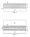
- Figure 1 depicts a stack of metal layers in one embodiment of this invention.
- the metal stack layer is to form a horizontal interconnecting line in a multilayered structure.
- the aluminum layer 106 is the bulk conductor layer, deposited on the surface of a dielectric layer 101 formed on a semiconductor substrate (not shown).
- the aluminum layer is sandwiched by a titanium layer 102 on the bottom and a titanium layer 104 on the top.
- titanium nitride layer 108 Overlying the top titanium layer is a titanium nitride layer 108.
- the primary function that the titanium nitride layer 108 serves in this structure is an antireflection coating that aids in defining and forming the interconnecting metal line.
- the semiconductor substrate undergoes an annealing process at an elevated temperature.
- the resulting structure is depicted in Figure 2.
- FIG. 2 depicts the result of the annealing process, where the titanium layers and the aluminum layer react to form titanium aluminide (TiAl 3 ) layers 103 and 105.
- the titanium aluminide layers are advantageous as an etch stop, an electromigration barrier, and a barrier against aluminum extrusion into vias that are formed later in the manufacturing process.
- Figure 2 also depicts a dielectric layer 109 on top of the titanium nitride layer 108. Vias through which the metal stack 100 is electrically connected to the upper conductive layers (not shown) are formed in the dielectric layer 109 as shown in Figure 3.
- Figure 3 depicts two via holes at the completion of the via etch process.
- the dimensions in the drawing do not necessarily correspond to any actual via holes and are only for the purpose of illustration.
- the aspect ratio of via holes i.e. the ratio of the depth of the via hole 1 to the diameter of the via hole d, may vary.
- an integrated circuit device with 0.18 ⁇ m design rules may include via holes with aspect ratio ranging from 1.4 to 2.4.
- the via etch process may generate via holes that resemble one or both of the vias in Figure 3.
- Via hole 310 in the drawing depicts one type of via holes of which the integrity of the grain structure of the titanium aluminide layer at the bottom of the via hole is preserved and the titanium aluminide layer completely shields the underlying aluminum.
- Via hole 320 in the drawing depicts the second type of via holes of which grains of the titanium aluminide layer 105 are missing and the aluminum layer 106 is uncovered at the area of the missing grains.
- the titanium nitride layer 108 is usually removed by the etching process.
- Figure 4 depicts the portion of the integrated circuit device including via 320 at the completion of via metal deposition.
- the via metal includes a thin titanium layer 201, a thin titanium nitride layer 203 and a tungsten plug 205.
- the titanium nitride layer in this structure serves as a diffusion barrier.
- the function of the titanium will be described in more detail in the following sections.
- Titanium is a chemically active metallic element and serves at least two purposes in this structure.
- titanium readily bonds with the walls of the via holes and with the surface of the titanium nitride layer 203 and as a result good adhesion between the walls of the via hole and the titanium nitride layer 203 may be achieved.
- titanium reacts with and reduces metal oxide such as aluminum oxide (Al 2 O 3 ) that forms at the surface of the metal stack 100 at the bottom of the via holes.
- metal oxide such as aluminum oxide (Al 2 O 3 )
- Al 2 O 3 aluminum oxide
- the size of the titanium aluminide molecule is less than the volume sum of its constituent titanium and aluminum atoms.
- a void that is proportional to the volume of formed titanium aluminide will also form.
- Figure 4 depicts such a reaction that forms voids initiated at the area 200 where some grains from the titanium aluminide layer 105 are missing. If the condition is favorable for the reaction to continue, the void will grow in size and excessive growth of the voids will cause the semiconductor integrated circuit device to fail.
- the failure is detected at the integrated circuit manufacturer's factory before it is incorporated into an electronic system, it is counted as a yield loss. More seriously, the void may be small at the initial test stage and escape detection and subsequently, during actual operation in the field, continues to grow and eventually causes of the entire system to fail.
- the first is to maintain the integrity of the titanium aluminide layer 105 so the titanium layer 201 does not come in direct contact with the underlying aluminum.
- This approach is not always practical because in order to ensure the complete removal of dielectric material 109 from the via hole, a certain over etch is necessary in at the via etch process and this over-etch often damages the titanium aluminide layer 105, resulting in missing grains at the bottom of the via holes.
- a preferable approach to eliminate the over growth of the void is to reduce the amount of the titanium available for the reaction by limiting the thickness of the titanium layer 201.
- the titanium layer 201 when the titanium layer 201 is not thicker than about 100 ⁇ , no serious void formation will take place such that the reliability of the semiconductor integrated circuit may be compromised. When the titanium layer 201 is thinner than about 55 ⁇ , the void formation problem can be practically arrested.
Landscapes
- Internal Circuitry In Semiconductor Integrated Circuit Devices (AREA)
Applications Claiming Priority (2)
| Application Number | Priority Date | Filing Date | Title |
|---|---|---|---|
| US385824 | 2003-03-11 | ||
| US10/385,824 US6977437B2 (en) | 2003-03-11 | 2003-03-11 | Method for forming a void free via |
Publications (2)
| Publication Number | Publication Date |
|---|---|
| EP1458020A2 true EP1458020A2 (de) | 2004-09-15 |
| EP1458020A3 EP1458020A3 (de) | 2005-01-12 |
Family
ID=32771580
Family Applications (1)
| Application Number | Title | Priority Date | Filing Date |
|---|---|---|---|
| EP04100983A Withdrawn EP1458020A3 (de) | 2003-03-11 | 2004-03-10 | Methode zur Herstellung eines hohlraumfreien Vias |
Country Status (3)
| Country | Link |
|---|---|
| US (2) | US6977437B2 (de) |
| EP (1) | EP1458020A3 (de) |
| JP (1) | JP2004274065A (de) |
Families Citing this family (5)
| Publication number | Priority date | Publication date | Assignee | Title |
|---|---|---|---|---|
| US7170174B2 (en) * | 2004-08-24 | 2007-01-30 | Micron Technology, Inc. | Contact structure and contact liner process |
| US7517320B2 (en) * | 2006-06-30 | 2009-04-14 | Broncus Technologies, Inc. | Airway bypass site selection and treatment planning |
| US9034664B2 (en) | 2012-05-16 | 2015-05-19 | International Business Machines Corporation | Method to resolve hollow metal defects in interconnects |
| KR102262024B1 (ko) | 2017-04-03 | 2021-06-09 | 삼성전자주식회사 | 반도체 장치 |
| US9953927B1 (en) | 2017-04-26 | 2018-04-24 | Globalfoundries Inc. | Liner replacements for interconnect openings |
Family Cites Families (10)
| Publication number | Priority date | Publication date | Assignee | Title |
|---|---|---|---|---|
| JP2660359B2 (ja) * | 1991-01-30 | 1997-10-08 | 三菱電機株式会社 | 半導体装置 |
| US5360995A (en) | 1993-09-14 | 1994-11-01 | Texas Instruments Incorporated | Buffered capped interconnect for a semiconductor device |
| US5470790A (en) * | 1994-10-17 | 1995-11-28 | Intel Corporation | Via hole profile and method of fabrication |
| US6285082B1 (en) | 1995-01-03 | 2001-09-04 | International Business Machines Corporation | Soft metal conductor |
| US5600182A (en) | 1995-01-24 | 1997-02-04 | Lsi Logic Corporation | Barrier metal technology for tungsten plug interconnection |
| KR0165813B1 (ko) * | 1995-04-12 | 1999-02-01 | 문정환 | 접속홀의 플러그 형성 방법 |
| US5918149A (en) | 1996-02-16 | 1999-06-29 | Advanced Micro Devices, Inc. | Deposition of a conductor in a via hole or trench |
| US20020003306A1 (en) | 1998-06-26 | 2002-01-10 | Minh Van Ngo | Method for reducing stress-induced voids for 0.25u and smaller semiconductor chip technology by annealing interconnect lines and using low bias voltage and low interlayer dielectric deposition rate and semiconductor chip made thereby |
| US6261954B1 (en) * | 2000-02-10 | 2001-07-17 | Chartered Semiconductor Manufacturing, Ltd. | Method to deposit a copper layer |
| US6333261B1 (en) | 2000-06-01 | 2001-12-25 | United Microelectronics Corp. | Method for preventing aluminum intrusions |
-
2003
- 2003-03-11 US US10/385,824 patent/US6977437B2/en not_active Expired - Lifetime
-
2004
- 2004-03-10 JP JP2004067067A patent/JP2004274065A/ja active Pending
- 2004-03-10 EP EP04100983A patent/EP1458020A3/de not_active Withdrawn
-
2005
- 2005-02-07 US US11/053,313 patent/US7323409B2/en not_active Expired - Lifetime
Also Published As
| Publication number | Publication date |
|---|---|
| US20040178504A1 (en) | 2004-09-16 |
| US6977437B2 (en) | 2005-12-20 |
| US7323409B2 (en) | 2008-01-29 |
| US20050146035A1 (en) | 2005-07-07 |
| JP2004274065A (ja) | 2004-09-30 |
| EP1458020A3 (de) | 2005-01-12 |
Similar Documents
| Publication | Publication Date | Title |
|---|---|---|
| US5459353A (en) | Semiconductor device including interlayer dielectric film layers and conductive film layers | |
| US4937652A (en) | Semiconductor device and method of manufacturing the same | |
| US7399706B2 (en) | Manufacturing method of semiconductor device | |
| JP2811131B2 (ja) | 半導体装置の配線接続構造およびその製造方法 | |
| US6943111B2 (en) | Barrier free copper interconnect by multi-layer copper seed | |
| US9559058B2 (en) | Semiconductor device and method for manufacturing the same | |
| US6143672A (en) | Method of reducing metal voidings in 0.25 μm AL interconnect | |
| US6383914B1 (en) | Method of manufacturing an aluminum interconnect structure of a semiconductor device having <111> orientation | |
| US10008450B2 (en) | Oxidation resistant barrier metal process for semiconductor devices | |
| US20020154468A1 (en) | Method of forming a capacitor | |
| US6677647B1 (en) | Electromigration characteristics of patterned metal features in semiconductor devices | |
| US6977437B2 (en) | Method for forming a void free via | |
| US6617231B1 (en) | Method for forming a metal extrusion free via | |
| JPH0969607A (ja) | 半導体装置およびその製造方法 | |
| US8044491B2 (en) | Semiconductor device and method of manufacturing the same | |
| CN1913125A (zh) | 过孔底接触及其制造方法 | |
| JP2000150520A (ja) | 相互接続部、及び相互接続部の製造方法 | |
| JP3417193B2 (ja) | 半導体装置の製造方法 | |
| JPH0637042A (ja) | 半導体集積回路装置及びその製造方法 | |
| JPH0536693A (ja) | ヒロツクを抑えた半導体装置とヒロツク抑制方法 | |
| JPH0594960A (ja) | 半導体装置の製造方法 |
Legal Events
| Date | Code | Title | Description |
|---|---|---|---|
| PUAI | Public reference made under article 153(3) epc to a published international application that has entered the european phase |
Free format text: ORIGINAL CODE: 0009012 |
|
| AK | Designated contracting states |
Kind code of ref document: A2 Designated state(s): AT BE BG CH CY CZ DE DK EE ES FI FR GB GR HU IE IT LI LU MC NL PL PT RO SE SI SK TR |
|
| AX | Request for extension of the european patent |
Extension state: AL LT LV MK |
|
| PUAL | Search report despatched |
Free format text: ORIGINAL CODE: 0009013 |
|
| AK | Designated contracting states |
Kind code of ref document: A3 Designated state(s): AT BE BG CH CY CZ DE DK EE ES FI FR GB GR HU IE IT LI LU MC NL PL PT RO SE SI SK TR |
|
| AX | Request for extension of the european patent |
Extension state: AL LT LV MK |
|
| 17P | Request for examination filed |
Effective date: 20050712 |
|
| AKX | Designation fees paid |
Designated state(s): DE FR GB |
|
| 17Q | First examination report despatched |
Effective date: 20111221 |
|
| STAA | Information on the status of an ep patent application or granted ep patent |
Free format text: STATUS: THE APPLICATION IS DEEMED TO BE WITHDRAWN |
|
| 18D | Application deemed to be withdrawn |
Effective date: 20120703 |