EP1457804A1 - Electrostatic driving device for a flexible thin film and manufacturing method of the same - Google Patents
Electrostatic driving device for a flexible thin film and manufacturing method of the same Download PDFInfo
- Publication number
- EP1457804A1 EP1457804A1 EP04004994A EP04004994A EP1457804A1 EP 1457804 A1 EP1457804 A1 EP 1457804A1 EP 04004994 A EP04004994 A EP 04004994A EP 04004994 A EP04004994 A EP 04004994A EP 1457804 A1 EP1457804 A1 EP 1457804A1
- Authority
- EP
- European Patent Office
- Prior art keywords
- base
- holding member
- film
- electrode
- side facing
- Prior art date
- Legal status (The legal status is an assumption and is not a legal conclusion. Google has not performed a legal analysis and makes no representation as to the accuracy of the status listed.)
- Granted
Links
- 239000010409 thin film Substances 0.000 title claims abstract description 52
- 238000004519 manufacturing process Methods 0.000 title claims description 25
- 125000006850 spacer group Chemical group 0.000 claims abstract description 43
- 239000010408 film Substances 0.000 claims description 56
- 239000000853 adhesive Substances 0.000 claims description 50
- 230000001070 adhesive effect Effects 0.000 claims description 50
- 239000000758 substrate Substances 0.000 claims description 48
- 238000000034 method Methods 0.000 claims description 8
- 229920001296 polysiloxane Polymers 0.000 claims description 3
- 239000004033 plastic Substances 0.000 description 17
- 239000002245 particle Substances 0.000 description 15
- 239000010931 gold Substances 0.000 description 8
- 229920001721 polyimide Polymers 0.000 description 8
- 229910052751 metal Inorganic materials 0.000 description 7
- 239000002184 metal Substances 0.000 description 7
- PXHVJJICTQNCMI-UHFFFAOYSA-N nickel Substances [Ni] PXHVJJICTQNCMI-UHFFFAOYSA-N 0.000 description 7
- 239000003795 chemical substances by application Substances 0.000 description 6
- 238000007650 screen-printing Methods 0.000 description 6
- 230000003287 optical effect Effects 0.000 description 5
- 239000013464 silicone adhesive Substances 0.000 description 5
- 229920001187 thermosetting polymer Polymers 0.000 description 5
- 239000004642 Polyimide Substances 0.000 description 4
- 229910052782 aluminium Inorganic materials 0.000 description 4
- XAGFODPZIPBFFR-UHFFFAOYSA-N aluminium Chemical compound [Al] XAGFODPZIPBFFR-UHFFFAOYSA-N 0.000 description 4
- 229910021421 monocrystalline silicon Inorganic materials 0.000 description 4
- XUIMIQQOPSSXEZ-UHFFFAOYSA-N Silicon Chemical compound [Si] XUIMIQQOPSSXEZ-UHFFFAOYSA-N 0.000 description 3
- 238000005452 bending Methods 0.000 description 3
- 239000007788 liquid Substances 0.000 description 3
- 239000000203 mixture Substances 0.000 description 3
- 229910052759 nickel Inorganic materials 0.000 description 3
- 229920002120 photoresistant polymer Polymers 0.000 description 3
- 238000003825 pressing Methods 0.000 description 3
- 229910052710 silicon Inorganic materials 0.000 description 3
- 239000010703 silicon Substances 0.000 description 3
- 230000001276 controlling effect Effects 0.000 description 2
- 239000011521 glass Substances 0.000 description 2
- VYZAMTAEIAYCRO-UHFFFAOYSA-N Chromium Chemical compound [Cr] VYZAMTAEIAYCRO-UHFFFAOYSA-N 0.000 description 1
- RYGMFSIKBFXOCR-UHFFFAOYSA-N Copper Chemical compound [Cu] RYGMFSIKBFXOCR-UHFFFAOYSA-N 0.000 description 1
- 239000004593 Epoxy Substances 0.000 description 1
- BQCADISMDOOEFD-UHFFFAOYSA-N Silver Chemical compound [Ag] BQCADISMDOOEFD-UHFFFAOYSA-N 0.000 description 1
- 230000001413 cellular effect Effects 0.000 description 1
- 229910052804 chromium Inorganic materials 0.000 description 1
- 239000011651 chromium Substances 0.000 description 1
- 229910052802 copper Inorganic materials 0.000 description 1
- 239000010949 copper Substances 0.000 description 1
- PCHJSUWPFVWCPO-UHFFFAOYSA-N gold Chemical compound [Au] PCHJSUWPFVWCPO-UHFFFAOYSA-N 0.000 description 1
- 229910052737 gold Inorganic materials 0.000 description 1
- 238000010438 heat treatment Methods 0.000 description 1
- 239000002923 metal particle Substances 0.000 description 1
- 150000002739 metals Chemical class 0.000 description 1
- 230000001105 regulatory effect Effects 0.000 description 1
- 239000004065 semiconductor Substances 0.000 description 1
- 229910052709 silver Inorganic materials 0.000 description 1
- 239000004332 silver Substances 0.000 description 1
Images




Classifications
-
- G—PHYSICS
- G02—OPTICS
- G02B—OPTICAL ELEMENTS, SYSTEMS OR APPARATUS
- G02B26/00—Optical devices or arrangements for the control of light using movable or deformable optical elements
- G02B26/08—Optical devices or arrangements for the control of light using movable or deformable optical elements for controlling the direction of light
- G02B26/0816—Optical devices or arrangements for the control of light using movable or deformable optical elements for controlling the direction of light by means of one or more reflecting elements
- G02B26/0825—Optical devices or arrangements for the control of light using movable or deformable optical elements for controlling the direction of light by means of one or more reflecting elements the reflecting element being a flexible sheet or membrane, e.g. for varying the focus
Definitions
- the spacers 115 formed of the thick-film photoresist are heated and softened.
- a pressure is added to the softened spacers 115 through the upper substrate 101 and lower substrate 102.
- the substrate interval between the upper substrate 101 and lower substrate 102 can be set to a desired value.
- the substrate interval requires a high precision. Therefore, it is necessary to use expensive bonding devices capable of controlling the pressure with the high precision such as a flip chip bonder.
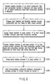
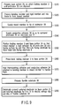
- a mixture ratio of the bonding member and rigid members (plastic particulates) prepared in the mixing step S120 is determined so that the plastic particulates are scattered with this density at the screen printing time. Thereafter, when the metal mask is removed, the mixed member remains in a predetermined position of the base 7. With the use of the screen printing, the mixed member can be supplied to the desired position of the base 7 with good precision.
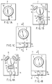
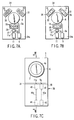
- the bonding spacer member keeps the interval between the holding member 3 and base 15, and not only bonds these but also conducts the film-side facing electrode 5a to the external electrode 11.
- the manufacturing method described with reference to FIG. 3 includes the step of supplying the conductive adhesive 12 onto the electrode pad 10 for this conduction, but the manufacturing method of the present embodiment does not require this step. Therefore, good productivity is obtained.
- the electrostatic driving device includes a flexible substrate 38.
- the flexible substrate 38 includes a polyimide substrate 39 formed of polyimide.
- two intermediate electrodes 41 and 42, two external electrodes 43 and 44, and two electric wirings 44a and 43a for electrically connecting the intermediate electrodes 41 and 42 to the external electrodes 43 and 44 are disposed.
- the electric wirings 44a and 43a are electrically connected to the external electrode 9 and external electrode 11 with an anisotropic conductive adhesive 37 through the intermediate electrodes 41 and 42.
- the anisotropic conductive adhesive 37 contains epoxy-based adhesive and conductive particles formed of nickel.
- the anisotropic conductive adhesive 37 may also contain particles plated with nickel or gold in the plastic particles instead of the conductive particles of nickel.
- the electric wirings 44a and 43a are formed of copper.
- the rigid members are spherical, but the rigid members are not limited to this, and other shapes such as a columnar shape and a plate like shape may also be used.
Landscapes
- Physics & Mathematics (AREA)
- General Physics & Mathematics (AREA)
- Optics & Photonics (AREA)
- Mechanical Light Control Or Optical Switches (AREA)
- Micromachines (AREA)
- Optical Elements Other Than Lenses (AREA)
Abstract
Description
Claims (14)
- An electrostatic driving device comprising:characterized in thata flexible thin film;a holding member, which holds the flexible thin film and allows the flexible thin film to bend;a function member disposed on the flexible thin film;a film-side facing electrode disposed on the flexible thin film;a base, which faces the holding member; anda base-side facing electrode, which is disposed on the base and faces the film-side facing electrode,
a bonding spacer member, which is held between the holding member and base, bonds the holding member to the base, and holds an interval between the holding member and base at a predetermined interval so as to keep an electrode interval between the film-side facing electrode and base-side facing electrode at a predetermined interval. - The electrostatic driving device according to claim 1, characterized in that the bonding spacer member includes a bonding member, which bonds the holding member and base, and rigid members, which have rigidity, and the rigid members keep the interval between the holding member and base at the predetermined interval.
- The electrostatic driving device according to claim 2, characterized in that the bonding member comprises only a portion that continuously extends around the film-side facing electrode and base-side facing electrode so that the rigid members are scattered in that portion.
- The electrostatic driving device according to claim 2, characterized in that the bonding member comprises portions that are spatially separated and located around the film-side facing electrode and base-side facing electrode and individually include at least one of the rigid members.
- The electrostatic driving device according to claim 2, characterized in that at least one of the bonding member and rigid members included in the bonding spacer member has conductivity, and
the electrostatic driving device characterized by further comprising:a film-side connecting member, which is disposed on the holding member and electrically connects the film-side facing electrode to the bonding spacer member;a first external electrode that is prepared for the flexible thin film, the first external electrode being disposed on the base; anda base-side connecting member, which is disposed on the base and electrically connects the first external electrode to the bonding spacer member. - The electrostatic driving device according to claim 5, characterized by further comprising:characterized in that the first external electrode and second external electrode are electrically connected to the electric wirings of the flexible substrate.a second external electrode that is prepared for the base, the second external electrode being electrically connected to the base-side facing electrode; anda flexible substrate including electric wirings,
- The electrostatic driving device according to claim 2, characterized in that the rigid members are spherical.
- The electrostatic driving device according to claim 2, characterized in that the bonding member contains an adhesive that hardens at normal temperature.
- The electrostatic driving device according to claim 8, characterized in that the bonding member contains a low-elasticity silicone-based adhesive.
- The electrostatic driving device according to claim 1 or claim 2, characterized by further comprising protrusions that are positioned between the holding member and base and protrude from one of the holding member and base, the other of the holding member and base including a facing surface that faces the tips of the protrusions, and
characterized in that the bonding spacer member is held between the tip of the protrusion and the facing surface. - A method of manufacturing a electrostatic driving device including: a flexible thin film; a holding member, which holds the flexible thin film and allows the flexible thin film to bend; a function member disposed on the flexible thin film; a film-side facing electrode disposed on the flexible thin film; a base, which faces the holding member; a base-side facing electrode, which is disposed on the base and faces the film-side facing electrode; and a bonding spacer member, which is held between the holding member and base, bonds the holding member to the base, and holds an interval between the holding member and base at a predetermined interval so as to keep an electrode interval between the film-side facing electrode and base-side facing electrode at a predetermined interval, the method characterized by comprising:a member preparing step of preparing the holding member holding the flexible thin film, on which the function member and film-side facing electrode are disposed, and the base, on which the base-side facing electrode is disposed;a mixing step of preparing an adhesive-containing bonding member and rigid members having rigidity, and mixing the prepared bonding member and rigid members so that the rigid members is scattered in the bonding member to form a mixed member including the mixed bonding member and rigid members;a supplying step of supplying the mixed member to one of the prepared holding member and base;a positioning step of positioning the holding member and base so that the supplied mixed member is held between the holding member and base, and that the film-side facing electrode faces the base-side facing electrode;a press-bonding step of press-bonding the positioned holding member and base; anda hardening step of hardening the adhesive contained in the bonding member in the mixed member held between the holding member and base so that the mixed member held between the holding member and base forms the bonding spacer member, the hardened mixed member forming the bonding spacer member.
- The manufacturing method according to claim 11, characterized in that a conductive film-side connecting member electrically connected to the film-side facing electrode is further disposed on the holding member prepared in the member preparing;
an external electrode for the film, and a conductive base-side connecting member electrically connected to the external electrode for the film are disposed on the base prepared in the member preparing step,
at least one of the bonding member and rigid members prepared in the mixing step has a conductivity,
the mixed member supplied in the supplying step is supplied to the holding member so as to contact the film-side connecting member or is supplied to the base so as to contact the base-side connecting member, and
in the positioning step, the holding member and base are positioned so that the supplied mixed member contacts the film-side connecting member and base-side connecting member and that the film-side facing electrode faces the base-side facing electrode. - The manufacturing method according to claim 12, characterized in that, in the member preparing step, a first external electrode that is prepared for the flexible thin film is further disposed on the holding member, the first external electrode being electrically connected to the film-side facing electrode, and a second external electrode that is prepared for the prepared base is further disposed on the base, the electrically connected to the base-side facing electrode,
the manufacturing method comprising:a flexible substrate preparing step of preparing a flexible substrate including electric wirings; anda connecting step of electrically connecting the first external electrode and second external electrode film to the electric wirings of the flexible substrate. - The manufacturing method according to claim 11, characterized in that one of the holding member and base prepared in the member preparing step has protrusions protruding from the one toward the other, the protrusions being positioned between the holding member and base when the holding member and base are positioned, and the other of the holding member and base includes a facing surface facing the tips of the protrusions when the holding member and base are positioned,
in the supplying step comprises, the mixed member is supplied to the tips of the protrusions, and
in the positioning step, the holding member and base are positioned so that the supplied mixed member is held between the tips of the protrusions and the facing surface and that the film-side facing electrode faces the base-side facing electrode.
Applications Claiming Priority (2)
| Application Number | Priority Date | Filing Date | Title |
|---|---|---|---|
| JP2003068318 | 2003-03-13 | ||
| JP2003068318A JP4282346B2 (en) | 2003-03-13 | 2003-03-13 | Electrostatic drive device and manufacturing method thereof |
Publications (2)
| Publication Number | Publication Date |
|---|---|
| EP1457804A1 true EP1457804A1 (en) | 2004-09-15 |
| EP1457804B1 EP1457804B1 (en) | 2008-12-03 |
Family
ID=32767963
Family Applications (1)
| Application Number | Title | Priority Date | Filing Date |
|---|---|---|---|
| EP04004994A Expired - Lifetime EP1457804B1 (en) | 2003-03-13 | 2004-03-03 | Electrostatic driving device for a flexible thin film and manufacturing method of the same |
Country Status (4)
| Country | Link |
|---|---|
| US (1) | US7122937B2 (en) |
| EP (1) | EP1457804B1 (en) |
| JP (1) | JP4282346B2 (en) |
| DE (1) | DE602004018051D1 (en) |
Cited By (2)
| Publication number | Priority date | Publication date | Assignee | Title |
|---|---|---|---|---|
| WO2010011488A3 (en) * | 2008-07-22 | 2010-12-02 | Qualcomm Mems Technologies, Inc. | Spacer for mems device package |
| US9057872B2 (en) | 2010-08-31 | 2015-06-16 | Qualcomm Mems Technologies, Inc. | Dielectric enhanced mirror for IMOD display |
Families Citing this family (11)
| Publication number | Priority date | Publication date | Assignee | Title |
|---|---|---|---|---|
| JP4282346B2 (en) * | 2003-03-13 | 2009-06-17 | オリンパス株式会社 | Electrostatic drive device and manufacturing method thereof |
| US20060076634A1 (en) | 2004-09-27 | 2006-04-13 | Lauren Palmateer | Method and system for packaging MEMS devices with incorporated getter |
| US7259449B2 (en) | 2004-09-27 | 2007-08-21 | Idc, Llc | Method and system for sealing a substrate |
| DE112006002428A5 (en) * | 2005-09-14 | 2008-12-11 | Htc Beteiligungs Gmbh | Flip-chip module and method for generating a flip-chip module |
| US20070065131A1 (en) * | 2005-09-20 | 2007-03-22 | Chengping Wei | Auto-focusing and Zooming Systems and Method of Operating Same |
| US7433555B2 (en) * | 2006-05-22 | 2008-10-07 | Visera Technologies Company Ltd | Optoelectronic device chip having a composite spacer structure and method making same |
| JP2008122723A (en) * | 2006-11-14 | 2008-05-29 | Topcon Corp | Deformable mirror and manufacturing method thereof |
| US9401461B2 (en) | 2007-07-11 | 2016-07-26 | Cree, Inc. | LED chip design for white conversion |
| US10505083B2 (en) * | 2007-07-11 | 2019-12-10 | Cree, Inc. | Coating method utilizing phosphor containment structure and devices fabricated using same |
| US8379392B2 (en) | 2009-10-23 | 2013-02-19 | Qualcomm Mems Technologies, Inc. | Light-based sealing and device packaging |
| KR102156765B1 (en) * | 2013-12-13 | 2020-09-16 | 엘지디스플레이 주식회사 | Organic Emitting Display Device and Method for Manufacturing the Same |
Citations (3)
| Publication number | Priority date | Publication date | Assignee | Title |
|---|---|---|---|---|
| US4973131A (en) * | 1989-02-03 | 1990-11-27 | Mcdonnell Douglas Corporation | Modulator mirror |
| US20020054422A1 (en) * | 2000-11-03 | 2002-05-09 | Carr Dustin W. | Packaged MEMs device and method for making the same |
| US20020057506A1 (en) * | 2000-11-16 | 2002-05-16 | Olympus Optical Co., Ltd. | Variable shape mirror and its manufacturing method |
Family Cites Families (3)
| Publication number | Priority date | Publication date | Assignee | Title |
|---|---|---|---|---|
| JP2872736B2 (en) * | 1990-03-27 | 1999-03-24 | 積水ファインケミカル株式会社 | Manufacturing method of liquid crystal display element |
| US6674562B1 (en) * | 1994-05-05 | 2004-01-06 | Iridigm Display Corporation | Interferometric modulation of radiation |
| JP4282346B2 (en) * | 2003-03-13 | 2009-06-17 | オリンパス株式会社 | Electrostatic drive device and manufacturing method thereof |
-
2003
- 2003-03-13 JP JP2003068318A patent/JP4282346B2/en not_active Expired - Lifetime
-
2004
- 2004-03-03 EP EP04004994A patent/EP1457804B1/en not_active Expired - Lifetime
- 2004-03-03 DE DE602004018051T patent/DE602004018051D1/en not_active Expired - Fee Related
- 2004-03-08 US US10/795,770 patent/US7122937B2/en not_active Expired - Fee Related
Patent Citations (3)
| Publication number | Priority date | Publication date | Assignee | Title |
|---|---|---|---|---|
| US4973131A (en) * | 1989-02-03 | 1990-11-27 | Mcdonnell Douglas Corporation | Modulator mirror |
| US20020054422A1 (en) * | 2000-11-03 | 2002-05-09 | Carr Dustin W. | Packaged MEMs device and method for making the same |
| US20020057506A1 (en) * | 2000-11-16 | 2002-05-16 | Olympus Optical Co., Ltd. | Variable shape mirror and its manufacturing method |
Cited By (2)
| Publication number | Priority date | Publication date | Assignee | Title |
|---|---|---|---|---|
| WO2010011488A3 (en) * | 2008-07-22 | 2010-12-02 | Qualcomm Mems Technologies, Inc. | Spacer for mems device package |
| US9057872B2 (en) | 2010-08-31 | 2015-06-16 | Qualcomm Mems Technologies, Inc. | Dielectric enhanced mirror for IMOD display |
Also Published As
| Publication number | Publication date |
|---|---|
| US20040189143A1 (en) | 2004-09-30 |
| JP4282346B2 (en) | 2009-06-17 |
| JP2004282839A (en) | 2004-10-07 |
| DE602004018051D1 (en) | 2009-01-15 |
| EP1457804B1 (en) | 2008-12-03 |
| US7122937B2 (en) | 2006-10-17 |
Similar Documents
| Publication | Publication Date | Title |
|---|---|---|
| EP1457804B1 (en) | Electrostatic driving device for a flexible thin film and manufacturing method of the same | |
| JP3540281B2 (en) | Imaging device | |
| KR100344726B1 (en) | Semiconductor device | |
| EP0662256B1 (en) | An electrical connecting structure and a method for electrically connecting terminals to each other | |
| JP2001230511A (en) | Connection structure, electro-optical device and electronic equipment | |
| CN101083238A (en) | Microelectronic element with elastic conductive projection and method of manufacture | |
| US20040099959A1 (en) | Conductive bump structure | |
| JP2008135719A (en) | Semiconductor module, semiconductor module manufacturing method, and portable device | |
| JPH08181172A (en) | Device having peak type dielectric dam and method of manufacturing the same | |
| JPS60191228A (en) | Connecting structure of display device | |
| JP5125314B2 (en) | Electronic equipment | |
| US20120104633A1 (en) | Electronic device and electronic apparatus | |
| JP4771658B2 (en) | Semiconductor device with compliant electrical terminal, apparatus including semiconductor device, and manufacturing method thereof | |
| JP2013030789A (en) | Packaging structure and manufacturing method therefor | |
| EP1391922A2 (en) | Semiconductor device mounting method, semiconductor device mounting structure, electro optical device, electro-optical device manufacturing method and electronic device | |
| JP2001326879A (en) | Display driver module and method of manufacturing the same | |
| TW200903577A (en) | Method for implementing semiconductor device | |
| JP3162068B2 (en) | Semiconductor chip mounting method | |
| JPS63122133A (en) | Electrically connecting method for semiconductor chip | |
| JP2001230001A (en) | Connection structure, electro-optical device and electronic equipment | |
| JP2001177081A (en) | Semiconductor device | |
| JP2007165744A (en) | Semiconductor device, mounting structure, electro-optical device, semiconductor device manufacturing method, mounting structure manufacturing method, electro-optical device manufacturing method, and electronic apparatus | |
| JP2007165745A (en) | Mounting structure, electro-optical device, and electronic apparatus | |
| TWI287265B (en) | Flip chip device | |
| JP2002134557A (en) | Semiconductor chip mounting method and semiconductor chip mounting structure |
Legal Events
| Date | Code | Title | Description |
|---|---|---|---|
| PUAI | Public reference made under article 153(3) epc to a published international application that has entered the european phase |
Free format text: ORIGINAL CODE: 0009012 |
|
| AK | Designated contracting states |
Kind code of ref document: A1 Designated state(s): AT BE BG CH CY CZ DE DK EE ES FI FR GB GR HU IE IT LI LU MC NL PL PT RO SE SI SK TR |
|
| AX | Request for extension of the european patent |
Extension state: AL LT LV MK |
|
| 17P | Request for examination filed |
Effective date: 20041216 |
|
| AKX | Designation fees paid |
Designated state(s): DE FR GB |
|
| GRAP | Despatch of communication of intention to grant a patent |
Free format text: ORIGINAL CODE: EPIDOSNIGR1 |
|
| GRAS | Grant fee paid |
Free format text: ORIGINAL CODE: EPIDOSNIGR3 |
|
| GRAA | (expected) grant |
Free format text: ORIGINAL CODE: 0009210 |
|
| AK | Designated contracting states |
Kind code of ref document: B1 Designated state(s): DE FR GB |
|
| REG | Reference to a national code |
Ref country code: GB Ref legal event code: FG4D |
|
| REF | Corresponds to: |
Ref document number: 602004018051 Country of ref document: DE Date of ref document: 20090115 Kind code of ref document: P |
|
| PGFP | Annual fee paid to national office [announced via postgrant information from national office to epo] |
Ref country code: GB Payment date: 20090225 Year of fee payment: 6 |
|
| PGFP | Annual fee paid to national office [announced via postgrant information from national office to epo] |
Ref country code: DE Payment date: 20090331 Year of fee payment: 6 |
|
| PLBE | No opposition filed within time limit |
Free format text: ORIGINAL CODE: 0009261 |
|
| STAA | Information on the status of an ep patent application or granted ep patent |
Free format text: STATUS: NO OPPOSITION FILED WITHIN TIME LIMIT |
|
| PGFP | Annual fee paid to national office [announced via postgrant information from national office to epo] |
Ref country code: FR Payment date: 20090227 Year of fee payment: 6 |
|
| 26N | No opposition filed |
Effective date: 20090904 |
|
| GBPC | Gb: european patent ceased through non-payment of renewal fee |
Effective date: 20100303 |
|
| REG | Reference to a national code |
Ref country code: FR Ref legal event code: ST Effective date: 20101130 |
|
| PG25 | Lapsed in a contracting state [announced via postgrant information from national office to epo] |
Ref country code: FR Free format text: LAPSE BECAUSE OF NON-PAYMENT OF DUE FEES Effective date: 20100331 |
|
| PG25 | Lapsed in a contracting state [announced via postgrant information from national office to epo] |
Ref country code: DE Free format text: LAPSE BECAUSE OF NON-PAYMENT OF DUE FEES Effective date: 20101001 |
|
| PG25 | Lapsed in a contracting state [announced via postgrant information from national office to epo] |
Ref country code: GB Free format text: LAPSE BECAUSE OF NON-PAYMENT OF DUE FEES Effective date: 20100303 |