EP1447908B1 - Power amplifier - Google Patents
Power amplifier Download PDFInfo
- Publication number
- EP1447908B1 EP1447908B1 EP02775506A EP02775506A EP1447908B1 EP 1447908 B1 EP1447908 B1 EP 1447908B1 EP 02775506 A EP02775506 A EP 02775506A EP 02775506 A EP02775506 A EP 02775506A EP 1447908 B1 EP1447908 B1 EP 1447908B1
- Authority
- EP
- European Patent Office
- Prior art keywords
- pulse
- signal
- output
- pulse modulation
- level
- Prior art date
- Legal status (The legal status is an assumption and is not a legal conclusion. Google has not performed a legal analysis and makes no representation as to the accuracy of the status listed.)
- Expired - Lifetime
Links
Images


Classifications
-
- H—ELECTRICITY
- H03—ELECTRONIC CIRCUITRY
- H03F—AMPLIFIERS
- H03F1/00—Details of amplifiers with only discharge tubes, only semiconductor devices or only unspecified devices as amplifying elements
- H03F1/26—Modifications of amplifiers to reduce influence of noise generated by amplifying elements
-
- H—ELECTRICITY
- H03—ELECTRONIC CIRCUITRY
- H03F—AMPLIFIERS
- H03F3/00—Amplifiers with only discharge tubes or only semiconductor devices as amplifying elements
- H03F3/20—Power amplifiers, e.g. Class B amplifiers, Class C amplifiers
- H03F3/21—Power amplifiers, e.g. Class B amplifiers, Class C amplifiers with semiconductor devices only
- H03F3/217—Class D power amplifiers; Switching amplifiers
- H03F3/2173—Class D power amplifiers; Switching amplifiers of the bridge type
-
- H—ELECTRICITY
- H03—ELECTRONIC CIRCUITRY
- H03F—AMPLIFIERS
- H03F3/00—Amplifiers with only discharge tubes or only semiconductor devices as amplifying elements
- H03F3/30—Single-ended push-pull [SEPP] amplifiers; Phase-splitters therefor
- H03F3/3001—Single-ended push-pull [SEPP] amplifiers; Phase-splitters therefor with field-effect transistors
- H03F3/3022—CMOS common source output SEPP amplifiers
- H03F3/3023—CMOS common source output SEPP amplifiers with asymmetrical driving of the end stage
- H03F3/3027—CMOS common source output SEPP amplifiers with asymmetrical driving of the end stage using a common source driving stage, i.e. inverting stage
-
- H—ELECTRICITY
- H03—ELECTRONIC CIRCUITRY
- H03F—AMPLIFIERS
- H03F2200/00—Indexing scheme relating to amplifiers
- H03F2200/331—Sigma delta modulation being used in an amplifying circuit
Definitions
- the present invention relates to power amplifiers.
- Class-D amplifiers serve as audio power amplifiers.
- the class-D 7 amplifiers amplify electric power by switching, and are structured, for example, as shown in Fig. 10 .
- a digital audio signal Pin is sent through an input terminal Tin to PWM (pulse width modulation) modulation circuits 11 and 12, and the input signal Pin is converted to a pair of PWM signals PA and PB.
- PWM pulse width modulation
- the pulse widths of the PWM signals PA and PB are changed according to the level (the level of each sample of the original analog signal converted to the signal Pin) indicated by the input signal Pin.
- the pulse width of one PWM signal PA has a magnitude corresponding to the level indicated by the input signal Pin
- the pulse width of the other PWM signal PB has a magnitude corresponding to the two's complement of the level indicated by the input signal Pin.
- their rising edges are fixed to the start point of one cycle period (reference period) Tc of the PWM signals PA and PB, and their falling edges are shifted according to the level indicated by the input signal Pin.
- fs 48 kHz
- Such a PWM signal PA is sent to a drive circuit 13, and a pair of drive voltages +PA and -PA which are the signal PA and a signal having the same level as the signal PA with the inverted polarities is formed as shown in Fig. 11A .
- These drive voltages +PA and -PA are sent to the gates of a pair of n-channel MOS-FETs (metal oxide semiconductor type field effect transistors) (Q11 and Q12).
- the FETs (Q11 and Q12) constitute a push-pull circuit 15.
- the drain of the FET (Q11) is connected to a power-supply terminal TPWR, the source of the FET (Q11) is connected to the drain of the FET (Q12), and the source of the FET (Q12) is connected to the ground.
- a stable DC voltage +VDD is supplied as a power-supply voltage.
- the voltage +VDD ranges, for example, from 20 V to 50 V.
- the source of the FET (Q11) and the drain of the FET (Q12) are connected to one end of a speaker 19 through a low-pass filter 17 formed of a coil and a capacitor.
- the PWM signal PB sent from the PWM modulation circuit 11 also passes through in the same way as the PWM signal PA. More specifically, the PWM signal PB is sent to a drive circuit 14, and a pair of drive voltages +PB and -PB which are the signal PB and a signal having the same level as the signal PB with the inverted polarities is formed as shown in Fig. 11B . These drive voltages +PB and -PB are sent to the gates of a pair of n-channel MOS-FETs (Q13 and Q14) constituting a push-pull circuit 16.
- the source of the FET (Q13) and the drain of the FET (Q14) are connected to the other end of the speaker 19 through a low-pass filter 18 formed of a coil and a capacitor.
- the periods when the current “i” flows is changed according to the periods when the original PWM signals PA and PB are at "H".
- the current "i” flows through the speaker 19
- the current "i” is integrated by the low-pass filters 17 and 18.
- the current "i” flowing through the speaker 19 is the analog current which corresponds to the level indicated by the input signal Pin and of which the electric power has been amplified. In other words, the electric-power-amplified output is sent to the speaker 19.
- the circuit shown in Fig. 10 functions as a power amplifier in this way.
- the FETs (Q11 to Q14) switch the power-supply voltage +VDD according to the input digital audio signal Pin to amplify the electric power. Therefore, a high efficiency and a large output are obtained.
- the carrier frequency Fc of the PWM signals PA and PB is, for example, 768 kHz as in the above case, and is included in the band of medium-wave broadcasting.
- An object of the present invention is to provide a power amplifier having a reduced level of such emission.
- a power amplifier comprising:
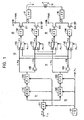
- Fig. 1 shows an example class-D power amplifier according to the present invention.
- a digital audio signal Pin is sent through an input terminal Tin to a ⁇ nodulation circuit 111.
- the ⁇ modulation circuit 111 constitutes a first PWM modulation circuit 11 together with a ROM (read only memory) 112 and a parallel-input-serial-output shift register 113, and constitutes a second PWM modulation circuit 12 together with a ROM 122 and a parallel-input-serial-output shift register 123.
- the digital audio signal Pin is converted to PWM signals +PA and +PB, such as those shown in Fig. 2A and Fig. 2B , by the PWM modulation circuits 11 and 12.
- the pulse widths of the PWM signals +PA and +PB are changed according to the level indicated by the input signal Pin.
- the pulse width of one PWM signal +PA has a magnitude corresponding to the level indicated by the input signal Pin
- the pulse width of the other PWM signal +PB has a magnitude corresponding to the two's complement, for example, of the level indicated by the input signal Pin.
- their rising edges are fixed to the start point of one cycle period Tc of the PWM signals +PA and +PB, and their falling edges are shifted according to the level indicated by the audio signal Pin.
- fs 48 kHz
- the digital audio signal is sent to the ROM 112, and is converted to parallel digital data corresponding to the quantization level.
- the parallel digital data is sent to the shift register 113, and is converted to a serial signal, that is, the PWM signal +PA.
- the digital audio signal output from the ⁇ modulation circuit 111 is sent to the ROM 122, and is converted to parallel digital data corresponding to the two's complement of the level of the digital audio signal.
- the parallel digital data is sent to the shift register 123, and is converted to a serial signal, that is, the PWM signal +PB.
- a timing-signal generation circuit 121 generates various timing signals, and sends the timing signals to the circuits 111 to 113, 122, and 123.
- the PWM signals +PA and +PB are sent to drive circuits 13 and 14 to generate drive voltages P1 to P4. More specifically, the PWM signal +PA is sent to selector circuits 131 and 142; is also sent to an inverter 135 to generate a level-inverted PWM signal -PA, as shown in Fig. 2A ; and the PWM signal -PA is sent to selector circuits 132 and 141.
- the PWM signal +PB is sent to the selector circuits 141, and 132; is also sent to an inverter 145 to generate a level-inverted PWM signal -PB, as shown in Fig. 2B ; and the PWM signal -PB is sent to the selector circuits 142 and 131.
- Fig. 2A and Fig. 2B are the same as Fig. 11A and Fig. 11B .
- the timing-signal generation circuit 121 outputs a signal Pc having a level inverted every cycle period Tc as shown in Fig. 2C , and the signal Pc is sent to the selector circuits 131, 132, 141, and 142 as a switching control signal.
- These drive voltages P1, P2, P3, and P4 are shaped by flip-flop circuits 133, 134, 143, and 144, and the drive voltages P1 and P2 are sent to the gates of a pair of switching elements, such as n-channel MOS-FETs (Q11 and Q12).
- the FETs (Q11 and Q12) constitute a push-pull circuit 15.
- the drain of the FET (Q11) is connected to a power-supply terminal TPWR
- the source of the FET (Q11) is connected to the drain of the FET (Q12)
- the source of the FET (Q12) is connected to the ground.
- a stable DC voltage +VDD such as a DC voltage ranging from 20 V to 50V, is supplied as a power-supply voltage.
- the source of the FET (Q11) and the drain of the FET (Q12) are connected to one end of a speaker 19 through a low-pass filter 17 formed, for example, of a coil and a capacitor.
- the drive voltages P3 and P4 sent from the drive circuit 14 also pass through in the same way as the drive voltages P1 and P2. More specifically, the drive voltages P3 and P4 are sent to a pair of n-channel MOS-FETs (Q13 and Q14) constituting a push-pull circuit 16.
- the source of the FET (Q13) and the drain of the FET (Q14) are connected to the other end of the speaker 19 through a low-pass filter 18 formed of a coil and a capacitor.
- the periods when the current "i” flows is changed according to the periods when the original PWM signals +PA and +PB are at "H".
- the current "i” flows through the speaker 19
- the current "i” is integrated by the low-pass filters 17 and 18.
- the current "i” flowing through the speaker 19 is the analog current which corresponds to the level indicated by the digital audio signal Pin and of which the electric power has been amplified. Therefore, the circuit shown in Fig. 1 functions as a class-D power amplifier, and the electric-power-amplified output is sent to the speaker 19.
- the power amplifier shown in Fig. 1 amplifies electric power by switching.
- the PWM signals +PA and +PB rise and fall once per cycle period Tc
- the output voltages VA and VB rise or fall once per cycle period Tc
- the number of the rising edges and the falling edges of the output voltages VA and VB is half the number of the rising edges and the falling edges of the output voltages VA and VB (see Fig. 11C and Fig. 11D ) in the power amplifier shown in Fig. 10 . Therefore, extraneous emission caused by the changes of the output voltages VA and VB is reduced.
- the frequency of the output voltages VA and VB is half the frequency of the output voltages VA and VB in the power amplifier shown in Fig. 10 , even when the power amplifier according to the present embodiment is united with a receiver as in a car audio system, or is disposed close to a receiver, disturbance given to broadcasting receiving, caused by the emission is reduced. Since disturbance given to broadcasting receiving, caused by the emission is reduced in this way, a member used for shielding a receiver from the emission can be eliminated, and cost is reduced. In addition, the power amplifier can be disposed close to a receiver, space is saved.
- both drive voltages P1 and P2 are "L" at a period although instantaneously.
- the FETs (Q11 and Q12) are both ON in this period, and current passes through the FETs (Q11 and Q12).
- the frequency of the drive voltages P1 to P4 in the power amplifier shown in Fig. 1 is half the frequency in the power amplifier shown in Fig. 10 , the number of times current passes through the FETs (Q11 and Q12) or the FETs (Q13 and Q14) when both FETs (Q11 and Q12) or both FETs (Q13 and Q14) are turned on at the same time is halved.
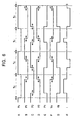
- the ROM 112 since a digital audio signal output from a ⁇ modulation circuit 111 has six bits per sampling, the ROM 112 has the address of seven bits A6 to A0, which is one-bit larger, as shown in Fig. 4 .
- the size of data at each address is 64 bits D63 to D0 corresponding to six bits per sampling.
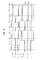
- the digital audio signal Since a digital audio signal output from a ⁇ modulation circuit 111 has six bits per sampling, the digital audio signal has one of 63 values from -31 through 0 to +31, as shown at the left-hand column of Fig. 5 . Since the 63 values are expressed by two's complements, they are shown in binary at the middle column of Fig. 5 . When it is assumed that these binary numbers are natural binary numbers and converted to decimal numbers, they have values as shown at the right-hand column of Fig. 5 .
- the same values are stored at the addresses 0 to 63 in the ROM 122 as those at the addresses 63 to 0 in the ROM 112.
- the same values are stored at the addresses 64 to 127 in the ROM 122 as those at the addresses 127 to 64 in the ROM 112.
- the data stored at the addresses 0 to 63 in the ROM 112 and ROM 122 can be stored at the addresses 0 to 63 in the ROM 112 and ROM 122 shown in Fig. 1 .
- a digital audio signal output from the ⁇ modulation circuit 111 is sent to the lower six bits A5 to A0, and the signal Pc, which is inverted every sample period Tc, is sent from a timing-signal generation circuit 121 to the most significant bit A6.
- the PWM signal P1 is sent to the gate of an FET (Q11) through a flip-flop circuit 133; and is also sent to an inverter 135, is inverted in level to generate a signal P2 as shown in Fig. 6D , and the signal P2 is sent to the gate of an FET (Q12) through a flip-flop circuit 134.
- the PWM signal P3 is sent to the gate of an FET (Q13) through a flip-flop circuit 143; and is also sent to an inverter 145, is inverted in level to generate a signal P4 as shown in Fig. 6E , and the signal P4 is sent to the gate of an FET (Q14) through a flip-flop circuit 144.
- a voltage VA generated at the connection point of the FETs (Q11 and Q12) and a voltage VB generated at the connection point of the FETs (Q13 and Q14) are the same as the voltages VA and VB shown in Fig. 2F and Fig. 2G , and current "i" shown in Fig. 6H flows through a speaker 19. As a result, an electric-power-amplified output is sent to the speaker 19.
- the power amplifier shown in Fig. 3 obtains the same advantages as the power amplifier shown in Fig. 1 , and in addition, can omit the selector circuits 131, 132, 141, and 142 shown in Fig. 1 .
- the output stage of each power amplifier is the BTL circuit.
- the output stage can be a single circuit.
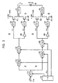
- Fig. 7 shows one form of such a power amplifier.
- PWM signals +PA and +PB are output from PWM conversion circuits 11 and 12, as shown in Fig. 8A ; the PWM signal +PA is sent to a drive circuit 13; the PWM signal +PB is sent to an inverter 145, and a PWM signal -PB having an inverted level as shown in Fig. 8B is generated; and the PWM signal - PB is sent to the drive circuit 13.
- the drive circuit 13 outputs drive voltages P1 and P2, and the drive voltages P1 and P2 are sent to a push-pull circuit 15.
- the drive voltage P1 is obtained by taking the PWM signal +PA and the PWM signal -PB alternately and at intervals equal to the cycle period Tc
- the drive voltage P2 is obtained by inverting the level of the drive voltage P1.
- the push-pull circuit 15 uses positive and negative power supplies.
- the drain of an FET (Q11) is connected to a positive-power-supply terminal TPWR+, and the source of an FET (Q12) is connected to a negative-power-supply terminal TPWR-.
- a pair of positive and negative DC voltages +VDD and -VDD are supplied to the power-supply terminals TPWR+ and TPWR- as power-supply voltages.
- the output end of the push-pull circuit 15 is connected to one end of a speaker 19 through a low-pass filter 17, and the other end of the speaker 19 is grounded.
- the output voltage VA of the push-pull circuit 15 has a shape such as that shown in Fig. 8D corresponding to the drive voltages P1 and P2.
- current "i" having a polarity and magnitude corresponding to an input signal Pin flows through the speaker 19, and electric power is amplified.
- a power amplifier shown in Fig. 9 has a single circuit at an output stage in the same way as the power amplifier shown in Fig. 7 , and uses only a DC voltage +VDD as a power-supply voltage for a push-pull circuit 15. Therefore, in this case, for example, a DC-cut capacitor 21 is connected between the output end of the push-pull circuit 15 and a low-pass filter 17.
- the input signal Pin is a digital audio signal.
- the input signal Pin may be an analog audio signal.
- the PWM signals +PA, +PB, -PA, and -PB may be PNM (pulse number modulation) signals.
- the PWM conversion circuits 11 and 12 can be formed of an increment counter, a decrement counter, and a comparison circuit.
- the power amplifiers are used as audio amplifiers.
- the power amplifiers can also be used as amplifiers for driving electric-power units such as motors.
- the power amplifiers can also be used as variable power-supply circuits.
- the number of the rising edges and the falling edges of the output voltage(s) is half the number of the rising edges and the falling edges of the PWM signals which generate the output voltage(s), emission caused by the change of the output voltage is reduced.
- a power amplifier according to the present invention is united with a receiver as in a car audio system or the power amplifier is disposed close to a receiver, disturbance given to broadcasting receiving, caused by the emission is reduced.
- a member used for shielding a receiver from the emission can be eliminated, and cost is reduced.
- a receiver can be disposed closer to the power amplifier, space is also reduced.
- the number of the rising edges and the falling edges of the output voltage (s) is halved, the number of times current flows through a push-pull circuit or push-pull circuits used for generating the output voltage(s) are also halved. A loss in the power amplifier is reduced, and heat generated by devices is also suppressed. In addition, since the number of times the output switching element(s) perform switching is reduced, the deterioration of audio characteristics, caused by switching noise is also suppressed.
Abstract
Description
- The present invention relates to power amplifiers.
- Class-D amplifiers serve as audio power amplifiers. The class-D7 amplifiers amplify electric power by switching, and are structured, for example, as shown in
Fig. 10 . - More specifically, a digital audio signal Pin is sent through an input terminal Tin to PWM (pulse width modulation)
modulation circuits - In this case, the pulse widths of the PWM signals PA and PB are changed according to the level (the level of each sample of the original analog signal converted to the signal Pin) indicated by the input signal Pin. As shown in
Fig. 12 , the pulse width of one PWM signal PA has a magnitude corresponding to the level indicated by the input signal Pin, and the pulse width of the other PWM signal PB has a magnitude corresponding to the two's complement of the level indicated by the input signal Pin. In the PWM signals PA and PB, their rising edges are fixed to the start point of one cycle period (reference period) Tc of the PWM signals PA and PB, and their falling edges are shifted according to the level indicated by the input signal Pin. - The carrier frequency fc (= 1/Tc) of the PWM signals PA and PB is set, for example, to 16 times the sampling frequency fs of the input digital audio signal Pin. When fs is 48 kHz, fc = 16fs = 16 x 48 kHz = 768 kHz.
- Such a PWM signal PA is sent to a
drive circuit 13, and a pair of drive voltages +PA and -PA which are the signal PA and a signal having the same level as the signal PA with the inverted polarities is formed as shown inFig. 11A . These drive voltages +PA and -PA are sent to the gates of a pair of n-channel MOS-FETs (metal oxide semiconductor type field effect transistors) (Q11 and Q12). In this case, the FETs (Q11 and Q12) constitute a push-pull circuit 15. The drain of the FET (Q11) is connected to a power-supply terminal TPWR, the source of the FET (Q11) is connected to the drain of the FET (Q12), and the source of the FET (Q12) is connected to the ground. To the power-supply terminal TPWR, a stable DC voltage +VDD is supplied as a power-supply voltage. The voltage +VDD ranges, for example, from 20 V to 50 V. - The source of the FET (Q11) and the drain of the FET (Q12) are connected to one end of a
speaker 19 through a low-pass filter 17 formed of a coil and a capacitor. - The PWM signal PB sent from the
PWM modulation circuit 11 also passes through in the same way as the PWM signal PA. More specifically, the PWM signal PB is sent to adrive circuit 14, and a pair of drive voltages +PB and -PB which are the signal PB and a signal having the same level as the signal PB with the inverted polarities is formed as shown inFig. 11B . These drive voltages +PB and -PB are sent to the gates of a pair of n-channel MOS-FETs (Q13 and Q14) constituting a push-pull circuit 16. - The source of the FET (Q13) and the drain of the FET (Q14) are connected to the other end of the
speaker 19 through a low-pass filter 18 formed of a coil and a capacitor. - Therefore, when +PA = "H", -PA = "L", the FET (Q11) is turned on, and the FET (Q12) is turned off. Consequently, a voltage VA generated at the connection point of the FETs (Q11 and Q12) is the voltage +VDD, as shown in
Fig. 11C . Conversely, when +PA = "L", -PA = "H", the FET (Q11) is turned off, and the FET (Q12) is turned on. Consequently, VA = 0. - In the same way, when +PB = "H", -PB = "L", the FET (Q13) is turned on, and the FET (Q14) is turned off. Consequently, a voltage VB generated at the connection point of the FETs (Q13 and Q14) is the voltage +VDD, as shown in
Fig. 11D . Conversely, when +PB = "L", -PB = "H", the FET - (Q13) is turned off, and the FET (Q14) is turned on. Consequently, VB = 0.
- In a period when VA = +VDD and VB = 0, as shown in
Fig. 10 andFig. 11E , current "i" flows from the connection point of the FETs (Q11 and Q12) to the connection point of the FETs (Q13 and Q14) through a line from the low-pass filter 17 through thespeaker 19 to the low-pass filter 18. - In a period when VA = 0 and VB = +VDD, the current "i" flows from the connection point of the FETs (Q13 and Q14) to the connection point of the FETs (Q11 and Q12) through a line from the low-
pass filter 18 through thespeaker 19 to the low-pass filter 17, in the direction reverse to that shown inFig. 10 . In a period when VA = VB = +VDD and in a period when VA = VB = 0, the current "i" does not flow. In other words, the push-pull circuits - The periods when the current "i" flows is changed according to the periods when the original PWM signals PA and PB are at "H". When the current "i" flows through the
speaker 19, the current "i" is integrated by the low-pass filters speaker 19 is the analog current which corresponds to the level indicated by the input signal Pin and of which the electric power has been amplified. In other words, the electric-power-amplified output is sent to thespeaker 19. - The circuit shown in
Fig. 10 functions as a power amplifier in this way. The FETs (Q11 to Q14) switch the power-supply voltage +VDD according to the input digital audio signal Pin to amplify the electric power. Therefore, a high efficiency and a large output are obtained. - Since the above-described power amplifier switches the power-supply voltage +VDD at a high speed to generate the output voltages VA and VB, as also shown in
Fig. 11C and Fig.11D , extraneous emission occurs at the rising edges and the falling edges of the output voltages VA and VB. In addition, when switching is achieved, since the power-supply voltage +VDD is as high as, for example, 20 V to 50 V, its emission level is quite high. The carrier frequency Fc of the PWM signals PA and PB is, for example, 768 kHz as in the above case, and is included in the band of medium-wave broadcasting. - Therefore, when a class-D power amplifier such as that described above is integrated with a receiver as in car audio systems or is disposed close to a receiver, emission caused at the rising edges and the falling edges of the output voltages VA and VB disturbs broadcasting receiving. Since the rising edges and the falling edges of the output voltages VA and VB are steep and include many harmonics, the harmonics are also emitted, which may disturb receiving at FM receivers and TV receivers.
- An object of the present invention is to provide a power amplifier having a reduced level of such emission.
- According to the present invention, there is provided a power amplifier comprising:
- pulse modulation means for supplying a first pulse signal and a second pulse signal;
- a first output circuit comprising a switching element, for supplying a switching output according to the first pulse signal sent from the pulse modulation means; and
- a second output circuit comprising a switching element, for supplying a switching output according to the second pulse signal sent from the pulse modulation means, and
- a load connected between an output end of the first output circuit and an output end of the second output circuit,
- characterised in that the first pulse signal is obtained by outputting alternately and at reference intervals equal to a reference period a first pulse modulation signal indicating the level of an input signal and a second inverted pulse modulation signal obtained by level-inverting a second pulse modulation signal which indicates the complement of the level of the input signal, and the second pulse signal is obtained by outputting *alternately and at the reference intervals the second pulse modulation signal indicating the complement of the level of the input signal (Pin) and a first inverted pulse modulation signal obtained by level-inverting the first pulse modulation signal which indicates the level of the input signal.
- Therefore, the number of the rising edges and the falling edges of the output voltages of the push-pull circuits is halved, and emission is reduced.
- Embodiments of the present invention will now be described with reference to the accompanying drawings, in which:
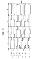
-
Fig. 1 is a systematic view showing an embodiment of the present invention. -
Fig. 2 is a waveform view used for describing a circuit shown inFig. 1 . -
Fig. 3 is a systematic view showing another embodiment of the present invention. -
Fig. 4 is a view showing an example data table. -
Fig. 5 is a view used for describing the relationship between a signal and an address. -
Fig. 6 is a waveform view used for describing a circuit shown inFig. 3 . -
Fig. 7 is a systematic view showing another embodiment of the present invention -
Fig. 8 is a waveform view used for describing a circuit shown inFig. 7 . -
Fig. 9 is a systematic view showing another embodiment of the present invention. -
Fig. 10 is a systematic view used for describing the present inversion. -
Fig. 11 is a waveform view used for describing a circuit shown inFig. 10 . -
Fig. 12 is a waveform view used for describing the circuit shown inFig. 10 . -
Fig. 1 shows an example class-D power amplifier according to the present invention. In this example, a digital audio signal Pin is sent through an input terminal Tin to aΔΣ nodulation circuit 111. TheΔΣ modulation circuit 111 constitutes a firstPWM modulation circuit 11 together with a ROM (read only memory) 112 and a parallel-input-serial-output shift register 113, and constitutes a secondPWM modulation circuit 12 together with aROM 122 and a parallel-input-serial-output shift register 123. The digital audio signal Pin is converted to PWM signals +PA and +PB, such as those shown inFig. 2A and Fig. 2B , by thePWM modulation circuits - In this case, the pulse widths of the PWM signals +PA and +PB are changed according to the level indicated by the input signal Pin. As shown in
Fig. 12 , the pulse width of one PWM signal +PA has a magnitude corresponding to the level indicated by the input signal Pin, and the pulse width of the other PWM signal +PB has a magnitude corresponding to the two's complement, for example, of the level indicated by the input signal Pin. In the PWM signals +PA and +PB, their rising edges are fixed to the start point of one cycle period Tc of the PWM signals +PA and +PB, and their falling edges are shifted according to the level indicated by the audio signal Pin. - The carrier frequency fc (= 1/Tc) of the PWM signals +PA and +PB is set, for example, to 16 times the sampling frequency fs of the digital audio signal Pin. When fs is 48 kHz, fc = 16fs = 16 x 48 kHz = 768 kHz.
- To generate such PWM signals +PA and +PB, in the
PWM modulation circuit 11, the digital audio signal Pin is sent from the input terminal Tin to theΔΣ modulation circuit 111, and is converted to a digital audio signal having reduced quantization noise in the audio frequency band while having a reduced number of bits, such as a digital audio signal having a quantization frequency (= fc) of 16fs and six quantization bits. The digital audio signal is sent to theROM 112, and is converted to parallel digital data corresponding to the quantization level. The parallel digital data is sent to theshift register 113, and is converted to a serial signal, that is, the PWM signal +PA. - In the
PWM modulation circuit 12, the digital audio signal output from theΔΣ modulation circuit 111 is sent to theROM 122, and is converted to parallel digital data corresponding to the two's complement of the level of the digital audio signal. The parallel digital data is sent to theshift register 123, and is converted to a serial signal, that is, the PWM signal +PB. - In this case, a timing-
signal generation circuit 121 generates various timing signals, and sends the timing signals to thecircuits 111 to 113, 122, and 123. - The PWM signals +PA and +PB are sent to drive
circuits selector circuits inverter 135 to generate a level-inverted PWM signal -PA, as shown inFig. 2A ; and the PWM signal -PA is sent toselector circuits selector circuits inverter 145 to generate a level-inverted PWM signal -PB, as shown inFig. 2B ; and the PWM signal -PB is sent to theselector circuits Fig. 2A and Fig. 2B are the same asFig. 11A and Fig. 11B . - Further, the timing-
signal generation circuit 121 outputs a signal Pc having a level inverted every cycle period Tc as shown inFig. 2C , and the signal Pc is sent to theselector circuits - Then, the
selector circuits Fig. 2D , the signals +PA and -PA as the drive voltages P1 and P2 during periods Tc when Pc = "L", and the signals -PB and +PB as the drive voltages P1 and P2 during periods Tc when Pc = "H". Theselector circuits Fig. 2E , the signals +PB and -PB as the drive voltages P3 and P4 during periods Tc when Pc = "L", and the signals -PA and +PA as the drive voltages P3 and P4 during periods Tc when Pc = "H". - These drive voltages P1, P2, P3, and P4 are shaped by flip-
flop circuits pull circuit 15. The drain of the FET (Q11) is connected to a power-supply terminal TPWR, the source of the FET (Q11) is connected to the drain of the FET (Q12), and the source of the FET (Q12) is connected to the ground. To the power-supply terminal TPWR, a stable DC voltage +VDD, such as a DC voltage ranging from 20 V to 50V, is supplied as a power-supply voltage. - The source of the FET (Q11) and the drain of the FET (Q12) are connected to one end of a
speaker 19 through a low-pass filter 17 formed, for example, of a coil and a capacitor. - The drive voltages P3 and P4 sent from the
drive circuit 14 also pass through in the same way as the drive voltages P1 and P2. More specifically, the drive voltages P3 and P4 are sent to a pair of n-channel MOS-FETs (Q13 and Q14) constituting a push-pull circuit 16. The source of the FET (Q13) and the drain of the FET (Q14) are connected to the other end of thespeaker 19 through a low-pass filter 18 formed of a coil and a capacitor. - With such a structure, when P1 = "H", P2 = "L", the FET (Q11) is turned on, and the FET (Q12) is turned off. Consequently, a voltage VA generated at the connection point of the FETs (Q11 and Q12) is the voltage +VDD, as shown in
Fig. 2F . - Conversely, when P1 = "L", P2 = "H", the FET (Q11) is turned off, and the FET (Q12) is turned on. Consequently, VA = 0.
- In the same way, when P3 = "H", P4 = "L", the FET (Q13) is turned on, and the FET (Q14) is turned off. Consequently, a voltage VB generated at the connection point of the FETs (Q13 and Q14) is the voltage +VDD, as shown in
Fig. 2G . Conversely, when P3 = "L", P4 = "H", the FET (Q13) is turned off, and the FET (Q14) is turned on. Consequently, VB = 0. - In a period when VA = +VDD and VB = 0, as shown in
Fig. 1 andFig. 2H , current "i" flows from the connection point of the FETs (Q11 and Q12) to the connection point of the FETs (Q13 and Q14) through a line from the low-pass filter 17 through thespeaker 19 to the low-pass filter 18. - In a period when VA = 0 and VB = +VDD, the current "i" flows from the connection point of the FETs (Q13 and Q14) to the connection point of the FETs (Q11 and Q12) through a line from the low-
pass filter 18 through thespeaker 19 to the low-pass filter 17, in the direction reverse to that shown inFig. 1 . In a period when VA = VB = +VDD and in a period when VA = VB = 0, the current "i" does not flow. In other words, the push-pull circuits - The periods when the current "i" flows is changed according to the periods when the original PWM signals +PA and +PB are at "H". When the current "i" flows through the
speaker 19, the current "i" is integrated by the low-pass filters speaker 19 is the analog current which corresponds to the level indicated by the digital audio signal Pin and of which the electric power has been amplified. Therefore, the circuit shown inFig. 1 functions as a class-D power amplifier, and the electric-power-amplified output is sent to thespeaker 19. - In this way, the power amplifier shown in
Fig. 1 amplifies electric power by switching. As also shown inFig. 2 , the PWM signals +PA and +PB rise and fall once per cycle period Tc, whereas the output voltages VA and VB rise or fall once per cycle period Tc, the number of the rising edges and the falling edges of the output voltages VA and VB is half the number of the rising edges and the falling edges of the output voltages VA and VB (seeFig. 11C and Fig. 11D ) in the power amplifier shown inFig. 10 . Therefore, extraneous emission caused by the changes of the output voltages VA and VB is reduced. - Since the frequency of the output voltages VA and VB is half the frequency of the output voltages VA and VB in the power amplifier shown in
Fig. 10 , even when the power amplifier according to the present embodiment is united with a receiver as in a car audio system, or is disposed close to a receiver, disturbance given to broadcasting receiving, caused by the emission is reduced. Since disturbance given to broadcasting receiving, caused by the emission is reduced in this way, a member used for shielding a receiver from the emission can be eliminated, and cost is reduced. In addition, the power amplifier can be disposed close to a receiver, space is saved. - Further, for example, in the push-
pull circuit 15, when the drive voltage P1 falls and the drive voltage P2 rises, if the drive voltage P1 falls with a delay, both drive voltages P1 and P2 are "L" at a period although instantaneously. The FETs (Q11 and Q12) are both ON in this period, and current passes through the FETs (Q11 and Q12). - Since the frequency of the drive voltages P1 to P4 in the power amplifier shown in
Fig. 1 is half the frequency in the power amplifier shown inFig. 10 , the number of times current passes through the FETs (Q11 and Q12) or the FETs (Q13 and Q14) when both FETs (Q11 and Q12) or both FETs (Q13 and Q14) are turned on at the same time is halved. - As clear also from
Fig. 2 , the drive voltages P1 and P2 in the periods when Pc = "H" are equivalent to the signal +PA and -PA obtained when the time axis is reversed, and the drive voltages P3 and P4 in the periods when Pc = "H" are equivalent to the signal +PB and -PB obtained when the time axis is reversed. - In
PWM modulation circuits Fig. 3 , when data read fromROMs Fig. 2 . - More specifically, in this case, since a digital audio signal output from a
ΔΣ modulation circuit 111 has six bits per sampling, theROM 112 has the address of seven bits A6 to A0, which is one-bit larger, as shown inFig. 4 . The size of data at each address is 64 bits D63 to D0 corresponding to six bits per sampling. - Since a digital audio signal output from a
ΔΣ modulation circuit 111 has six bits per sampling, the digital audio signal has one of 63 values from -31 through 0 to +31, as shown at the left-hand column ofFig. 5 . Since the 63 values are expressed by two's complements, they are shown in binary at the middle column ofFig. 5 . When it is assumed that these binary numbers are natural binary numbers and converted to decimal numbers, they have values as shown at the right-hand column ofFig. 5 . - As shown in
Fig. 4 , when an address number in theROM 112 is called "m" (0 ≤ m ≤ 127), the address corresponding to m = 32 is not used, and at the addresses corresponding to m = 33 to 63, the values having "1" from the most significant bit D63 to the bit D(96-m) and having "0" from the bit D(95-m) to the least significant bit D0 are prepared. At the addresses corresponding to m = 0 to 31, the values having "1" from the most significant bit D63 to the bit D(32-m) and having "0" from the bit D(31-m) to the least significant bit D0 are prepared. - Further, the address corresponding to m = (64 + 32) in the
ROM 112 is not used, and at the addresses corresponding to m = (64 + 33) to (64 + 63) and (64 + 0) to (64 + 31), the values obtained when the higher-order bits and the lower-order bits of the values at the addresses corresponding to m = 33 to 63 and 0 to 31 are transposed in their bit arrangement are prepared. More specifically, at the addresses corresponding to m = (64 + 33) to (64 + 63), the values having "0" from the most significant bit D63 to the bit D(m-96) and having "1" from the bit D(m-97) to the least significant bit D0 are prepared. At the addresses corresponding to m = (64 + 0) to (64 + 31), the values having "0" from the most significant bit D63 to the bit D(m-32) and having "1" from the bit D(m-33) to the least significant bit D0 are prepared. - Furthermore, the same values are stored at the
addresses 0 to 63 in theROM 122 as those at theaddresses 63 to 0 in theROM 112. The same values are stored at theaddresses 64 to 127 in theROM 122 as those at the addresses 127 to 64 in theROM 112. The data stored at theaddresses 0 to 63 in theROM 112 andROM 122 can be stored at theaddresses 0 to 63 in theROM 112 andROM 122 shown inFig. 1 . - As shown at the bottom of
Fig. 4 , among the seven-bit address A6 to A0 in theROM 112 andROM 122, a digital audio signal output from theΔΣ modulation circuit 111 is sent to the lower six bits A5 to A0, and the signal Pc, which is inverted every sample period Tc, is sent from a timing-signal generation circuit 121 to the most significant bit A6. - Therefore, as understood also from
Fig. 4 , since the most significant bit A6 of the address of theROM 112 is "0" at the periods Tc when Pc = "L", data D63 to D0 at the address corresponding to a digital audio signal sent from theΔΣ modulation circuit 111 is output among data at theaddresses 0 to 63. Since the most significant bit A6 of the address of theROM 112 is "1" at the periods Tc when Pc = "H", data D63 to D0 at the address corresponding to a digital audio signal sent from theΔΣ modulation circuit 111 is output among data at the addresses (64+0) to (64+63). Then, such data D63 to D0 is sent to a parallel-input-serial-output shift register 113, and is converted to a serial signal. - Therefore, as shown in
Fig. 6B , the serial signal obtained by the conversion is called a PWM signal P1; in periods Tc when Pc = "L", the serial signal has already risen at the start of each period Tc, and the falling point of the serial signal is changed according to the level indicated by the digital audio signal; and in periods Tc when Pc = "H", the rising point of the serial signal is changed according to the level indicated by the digital audio signal, and the serial signal has already risen at the end point of each period Tc. - In the
ROM 122, since the most significant bit of the address is "1" at the periods Tc when Pc = "L", data D63 to D0 at the address corresponding to an input digital audio signal is output among data at theaddresses 64 to 127. Since the most significant bit of the address is "0" at the periods Tc when Pc = "H", data D63 to D0 at the address corresponding to an input digital audio signal is output among data at theaddresses 0 to 63. Then, such data D63 to D0 is sent to a parallel-input-serial-output shift register 123, and is converted to a serial signal. - Therefore, as shown in
Fig. 6C , the serial signal obtained by the conversion is called a PWM signal P3; in periods Tc when Pc = "L", the serial signal has already risen at the start of each period Tc, and the falling point of the serial signal is changed according to the complement of the level indicated by the digital audio signal; and in periods Tc when Pc = "H", the rising point of the serial signal is changed according to the complement of the level indicated by the digital audio signal, and the serial signal has already risen at the end point of each period Tc. - Then, the PWM signal P1 is sent to the gate of an FET (Q11) through a flip-
flop circuit 133; and is also sent to aninverter 135, is inverted in level to generate a signal P2 as shown inFig. 6D , and the signal P2 is sent to the gate of an FET (Q12) through a flip-flop circuit 134. The PWM signal P3 is sent to the gate of an FET (Q13) through a flip-flop circuit 143; and is also sent to aninverter 145, is inverted in level to generate a signal P4 as shown inFig. 6E , and the signal P4 is sent to the gate of an FET (Q14) through a flip-flop circuit 144. - Therefore, as shown in
Fig. 6F and Fig. 6G , a voltage VA generated at the connection point of the FETs (Q11 and Q12) and a voltage VB generated at the connection point of the FETs (Q13 and Q14) are the same as the voltages VA and VB shown inFig. 2F and Fig. 2G , and current "i" shown inFig. 6H flows through aspeaker 19. As a result, an electric-power-amplified output is sent to thespeaker 19. - The power amplifier shown in
Fig. 3 obtains the same advantages as the power amplifier shown inFig. 1 , and in addition, can omit theselector circuits Fig. 1 . - In the foregoing description, the output stage of each power amplifier is the BTL circuit. The output stage can be a single circuit.
Fig. 7 shows one form of such a power amplifier. - More specifically, in the power amplifier shown in
Fig. 7 , PWM signals +PA and +PB are output fromPWM conversion circuits Fig. 8A ; the PWM signal +PA is sent to adrive circuit 13; the PWM signal +PB is sent to aninverter 145, and a PWM signal -PB having an inverted level as shown inFig. 8B is generated; and the PWM signal - PB is sent to thedrive circuit 13. - Then, the
drive circuit 13 outputs drive voltages P1 and P2, and the drive voltages P1 and P2 are sent to a push-pull circuit 15. In this case, as shown inFig. 8C , the drive voltage P1 is obtained by taking the PWM signal +PA and the PWM signal -PB alternately and at intervals equal to the cycle period Tc, and the drive voltage P2 is obtained by inverting the level of the drive voltage P1. - In the power amplifier shown in
Fig. 7 , the push-pull circuit 15 uses positive and negative power supplies. The drain of an FET (Q11) is connected to a positive-power-supply terminal TPWR+, and the source of an FET (Q12) is connected to a negative-power-supply terminal TPWR-. A pair of positive and negative DC voltages +VDD and -VDD are supplied to the power-supply terminals TPWR+ and TPWR- as power-supply voltages. The output end of the push-pull circuit 15 is connected to one end of aspeaker 19 through a low-pass filter 17, and the other end of thespeaker 19 is grounded. - Therefore, the output voltage VA of the push-
pull circuit 15 has a shape such as that shown inFig. 8D corresponding to the drive voltages P1 and P2. As shown inFig. 8E , current "i" having a polarity and magnitude corresponding to an input signal Pin flows through thespeaker 19, and electric power is amplified. - Also in this power amplifier, since the number of the rising edges and the falling edges of the drive voltages P1 and P2 is half the number of the rising edges and the falling edges of the PWM signals +PA and +PB, current flowing through the FETs (Q11 and Q12) are halved. In addition, since the frequency of the output voltage VA is halved, emission caused by the output voltage VA is also reduced.
- A power amplifier shown in
Fig. 9 has a single circuit at an output stage in the same way as the power amplifier shown inFig. 7 , and uses only a DC voltage +VDD as a power-supply voltage for a push-pull circuit 15. Therefore, in this case, for example, a DC-cut capacitor 21 is connected between the output end of the push-pull circuit 15 and a low-pass filter 17. - In the above description, the input signal Pin is a digital audio signal. The input signal Pin may be an analog audio signal. In addition, the PWM signals +PA, +PB, -PA, and -PB may be PNM (pulse number modulation) signals. Further, the
PWM conversion circuits - In the data table of the
ROMs Fig. 4 , when the higher-order bits and the lower-order bits of the data at theaddresses 0 to 63 are transposed in their bit arrangement, the data at theaddresses 64 to 127 is obtained. Therefore, when the order of taking out data loaded into the shift registers 113 and 123 is switched between from the least significant bit D0 and from the most significant bit D63 is switched between the periods Tc when Pc = "L" and the periods Tc when Pc = "H" to reverse the time axis in each period Tc, theROMs addresses 0 to 63. The capacity of theROMs - Furthermore, in the above description, the power amplifiers are used as audio amplifiers. The power amplifiers can also be used as amplifiers for driving electric-power units such as motors. When any load is connected instead of the
speaker 19, an operation voltage can be supplied to the load, and the level of the voltage supplied to the load can be changed by changing the input signal Pin. Therefore, the power amplifiers can also be used as variable power-supply circuits. - According to the present invention, since the number of the rising edges and the falling edges of the output voltage(s) is half the number of the rising edges and the falling edges of the PWM signals which generate the output voltage(s), emission caused by the change of the output voltage is reduced.
- Therefore, even if a power amplifier according to the present invention is united with a receiver as in a car audio system or the power amplifier is disposed close to a receiver, disturbance given to broadcasting receiving, caused by the emission is reduced. In addition, with this, a member used for shielding a receiver from the emission can be eliminated, and cost is reduced. Further, since a receiver can be disposed closer to the power amplifier, space is also reduced.
- Furthermore, since the number of the rising edges and the falling edges of the output voltage (s) is halved, the number of times current flows through a push-pull circuit or push-pull circuits used for generating the output voltage(s) are also halved. A loss in the power amplifier is reduced, and heat generated by devices is also suppressed. In addition, since the number of times the output switching element(s) perform switching is reduced, the deterioration of audio characteristics, caused by switching noise is also suppressed.
Claims (8)
- A power amplifier comprising:pulse modulation means (111, 112, 113, 135, 131, 132, 145, 141, 142) for supplying a first pulse signal (P1) and a second pulse signal (P3);a first output circuit (15) comprising a switching element (Q11, Q12), for supplying a switching output (VA) according to the first pulse signal (P1) sent from the pulse modulation means; anda second output circuit (16) comprising a switching element (Q 13, Q14), for supplying a switching output (VB) according to the second pulse signal (P3) sent from the pulse modulation means, anda load (17, 18, 19) connected between an output end of the first output circuit (15) and an output end of the second output circuit (16),characterised in that the pulse modulation means is adapted to obtain the first pulse signal by outputting alternately and at reference intervals equal to a reference period a first pulse modulation signal (+PA) indicating the level of an input signal and a second inverted pulse modulation signal (-PB) obtained by level-inverting a second pulse modulation signal (+PB) which indicates the complement of the level of the input signal, and to obtain the second pulse signal (P3) by outputting alternately and at the reference intervals the second pulse modulation signal (+PB) indicating the complement of the level of the input signal and a first inverted pulse modulation signal (-PA) obtained by level-inverting the first pulse modulation signal (+PA) which indicates the level of the input signal.
- A power amplifier according to claim 1, wherein
the pulse modulation means comprises:a first pulse modulation circuit (111, 112, 113) for converting the input signal to the first pulse modulation signal, indicating the level of the input signal, at the reference intervals to output it;a second pulse modulation circuit (111, 122, 123) for converting the input signal (Pin) to the second pulse modulation signal, indicating the complement of the level of the input signal, at the reference intervals to output it;a first inversion circuit (135) for level-inverting the output of the first pulse modulation circuit (111, 112, 113) to output the first inverted pulse modulation signal;a second inversion circuit (145) for level-inverting the output of the second pulse modulation circuit (111, 122, 123) to output the second inverted pulse modulation signal;a first selection circuit (131, 132) for selecting alternately and at the reference intervals the first pulse modulation signal and the second inverted pulse modulation signal to output the first pulse signal (P1, P2); anda second selection circuit (141, 142) for selecting alternately and at the reference intervals the second pulse modulation signal and the first inverted pulse modulation signal to output the second pulse signal. - A power amplifier according to claim 1, wherein
the pulse modulation means comprises:a memory (112, 122) for storing first pulse waveform data which indicates the level of the input signal; anda control circuit (121) for controlling reading from the memory, the control circuit (121) being arranged to change reading from the memory (112, 122), at the reference intervals to output the first and second pulse signals. - A power amplifier according to claim 3, wherein
the memory (112, 122) stores the first pulse waveform data, which indicates the level of the input signal, and second pulse waveform data which indicates the complement of the level of the input signal, and
the control circuit (121) is arranged to control reading from the memory (112, 122) so as to read alternately and at the reference intervals the first pulse waveform data and second inverted pulse waveform data obtained by level-inverting the second pulse waveform data, and so as to read alternately and at the reference intervals the second pulse waveform data and first inverted pulse waveform data obtained by level-inverting the first pulse waveform data. - A power amplifier according to claim 3, wherein the control circuit (121) is arranged to control reading from the memory (112, 122) so as to read alternately and at the reference intervals the first pulse waveform data and reverse-order pulse waveform data obtained by reading the first pulse waveform data in a reverse order, and so as to read alternately and at the reference intervals second inverted pulse waveform data obtained by level-inverting the reverse-order pulse waveform data, and first inverted pulse waveform data obtained by level-inverting the first pulse waveform data.
- A power amplifier according to claim 1, wherein
the pulse modulation means comprises:a first pulse modulation circuit (111, 112, 113) for converting the input signal to the first pulse modulation signal, indicating the level of the input signal, at the reference intervals to output it;a second pulse modulation circuit (111, 122, 123) for converting the input signal to the second pulse modulation signal, indicating the complement of the level of the input signal, at the reference intervals to output it;a first reverse circuit for reversing the time axis of the first pulse modulation signal to output a second time-reversed pulse modulation signal;a second reverse circuit for reversing the time axis of the second pulse modulation signal to output a first time-reversed pulse modulation signal;a first selection circuit (133, 134) for selecting alternately and at the reference intervals the first pulse modulation signal and the second time-reversed pulse modulation signal to output the first pulse signal; anda second selection circuit (143, 144) for selecting alternately at the reference intervals the second pulse modulation signal and the first time-reversed pulse modulation signal to output the second pulse signal. - A power amplifier according to any one of the preceding claims, wherein
the first and second output circuits (15, 16) are structured such that a pair of switching elements (Q11, Q12; Q13, Q14) are push-pull-connected;
the first pulse signal and a first inverted pulse signal obtained by level-inverting the first pulse signal are sent to the pair of switching elements (Q11, Q12) of the first output circuit (15); and
the second pulse signal and a second inverted pulse signal obtained by level-inverting the second pulse signal are sent to the pair of switching elements (Q13, Q14) of the second output circuit (16). - A power amplifier according to any one of the preceding claims, wherein the pulse modulation signals are PWM signals.
Applications Claiming Priority (5)
| Application Number | Priority Date | Filing Date | Title |
|---|---|---|---|
| JP2001352922 | 2001-11-19 | ||
| JP2001352922 | 2001-11-19 | ||
| JP2002162437A JP3894305B2 (en) | 2001-11-19 | 2002-06-04 | Power Amplifier |
| JP2002162437 | 2002-06-04 | ||
| PCT/JP2002/011597 WO2003044947A1 (en) | 2001-11-19 | 2002-11-07 | Power amplifier |
Publications (3)
| Publication Number | Publication Date |
|---|---|
| EP1447908A1 EP1447908A1 (en) | 2004-08-18 |
| EP1447908A4 EP1447908A4 (en) | 2006-02-01 |
| EP1447908B1 true EP1447908B1 (en) | 2011-03-16 |
Family
ID=26624594
Family Applications (1)
| Application Number | Title | Priority Date | Filing Date |
|---|---|---|---|
| EP02775506A Expired - Lifetime EP1447908B1 (en) | 2001-11-19 | 2002-11-07 | Power amplifier |
Country Status (6)
| Country | Link |
|---|---|
| US (1) | US6917242B2 (en) |
| EP (1) | EP1447908B1 (en) |
| JP (1) | JP3894305B2 (en) |
| KR (1) | KR100976444B1 (en) |
| DE (1) | DE60239484D1 (en) |
| WO (1) | WO2003044947A1 (en) |
Families Citing this family (18)
| Publication number | Priority date | Publication date | Assignee | Title |
|---|---|---|---|---|
| JP3894294B2 (en) * | 2001-11-19 | 2007-03-14 | ソニー株式会社 | Power Amplifier |
| WO2004010575A1 (en) * | 2002-07-18 | 2004-01-29 | Sony Corporation | Power amplifier |
| US7061312B2 (en) * | 2003-03-21 | 2006-06-13 | D2Audio Corporation | Systems and methods for providing multi channel pulse width modulated audio with staggered outputs |
| US7929718B1 (en) | 2003-05-12 | 2011-04-19 | D2Audio Corporation | Systems and methods for switching and mixing signals in a multi-channel amplifier |
| JP4154601B2 (en) * | 2003-10-23 | 2008-09-24 | ソニー株式会社 | Signal conversion device, output amplifier device, audio device, and transmission / reception system |
| JP4587222B2 (en) * | 2005-11-29 | 2010-11-24 | ローム株式会社 | Class D amplifier and audio equipment including the same |
| EP1985013A4 (en) * | 2006-01-24 | 2009-02-25 | D2Audio Corp | Systems and methods for improving performance in a digital amplifier by adding an ultrasonic signal to an input audio signal |
| JP4702296B2 (en) * | 2006-01-30 | 2011-06-15 | ヤマハ株式会社 | amplifier |
| CN101091307B (en) * | 2006-10-18 | 2011-01-26 | 埃派克森微电子有限公司 | Switch amplifier |
| TWI354439B (en) * | 2007-06-04 | 2011-12-11 | Holtek Semiconductor Inc | Ac signal producer and method thereof |
| US8072283B2 (en) * | 2007-09-04 | 2011-12-06 | Telefonaktiebolaget L M Ericsson (Publ) | Signal modulation for switched mode power amplifiers |
| JP2009147552A (en) * | 2007-12-12 | 2009-07-02 | Panasonic Corp | Class d amplifier |
| JP5099699B2 (en) * | 2008-05-16 | 2012-12-19 | 国立大学法人 名古屋工業大学 | Pulse width position modulation signal generator |
| CN102150368A (en) | 2008-11-28 | 2011-08-10 | 三菱电机株式会社 | Phase-compensated pulse width modulation circuit and digital/analog conversion device |
| US7986187B1 (en) * | 2010-03-04 | 2011-07-26 | Bose Corporation | Versatile audio power amplifier |
| EP2608403A1 (en) * | 2011-12-21 | 2013-06-26 | Alcatel Lucent | A method for signal modulation using pulse width modulators |
| US9559642B2 (en) | 2015-01-02 | 2017-01-31 | Logitech Europe, S.A. | Audio delivery system having an improved efficiency and extended operation time between recharges or battery replacements |
| WO2019204999A1 (en) * | 2018-04-25 | 2019-10-31 | Huawei Technologies Co., Ltd. | Method and apparatus for control of optical phase shifters in an optical device |
Family Cites Families (10)
| Publication number | Priority date | Publication date | Assignee | Title |
|---|---|---|---|---|
| DE3677229D1 (en) * | 1986-12-01 | 1991-02-28 | Itt Ind Gmbh Deutsche | POWER SWITCH. |
| US5398003A (en) * | 1994-03-30 | 1995-03-14 | Apple Computer, Inc. | Pulse width modulation speaker amplifier |
| US5617058A (en) * | 1995-11-13 | 1997-04-01 | Apogee Technology, Inc. | Digital signal processing for linearization of small input signals to a tri-state power switch |
| US6104248A (en) * | 1998-10-23 | 2000-08-15 | Carver; Robert W. | Audio amplifier with tracking power supply utilizing inductive power converters |
| NL1011002C2 (en) * | 1999-01-12 | 2000-07-20 | Univ Eindhoven Tech | Amplifier circuit. |
| JP2001185961A (en) | 1999-12-24 | 2001-07-06 | Alpine Electronics Inc | Digital amplifier |
| JP4387601B2 (en) | 2000-02-01 | 2009-12-16 | アルパイン株式会社 | Digital amplifier |
| KR20010105877A (en) * | 2000-05-19 | 2001-11-29 | 배길훈 | Solenoid valve of brake system for car |
| JP2002158544A (en) * | 2000-11-17 | 2002-05-31 | Sony Corp | Digital power amplifier |
| JP2002158549A (en) | 2000-11-17 | 2002-05-31 | Sony Corp | Digital power amplifier system |
-
2002
- 2002-06-04 JP JP2002162437A patent/JP3894305B2/en not_active Expired - Fee Related
- 2002-11-07 KR KR1020037008938A patent/KR100976444B1/en not_active IP Right Cessation
- 2002-11-07 EP EP02775506A patent/EP1447908B1/en not_active Expired - Lifetime
- 2002-11-07 DE DE60239484T patent/DE60239484D1/en not_active Expired - Lifetime
- 2002-11-07 US US10/466,927 patent/US6917242B2/en not_active Expired - Lifetime
- 2002-11-07 WO PCT/JP2002/011597 patent/WO2003044947A1/en active Application Filing
Also Published As
| Publication number | Publication date |
|---|---|
| DE60239484D1 (en) | 2011-04-28 |
| KR20040058096A (en) | 2004-07-03 |
| EP1447908A1 (en) | 2004-08-18 |
| JP2003218647A (en) | 2003-07-31 |
| JP3894305B2 (en) | 2007-03-22 |
| WO2003044947A1 (en) | 2003-05-30 |
| KR100976444B1 (en) | 2010-08-18 |
| US20040263244A1 (en) | 2004-12-30 |
| US6917242B2 (en) | 2005-07-12 |
| EP1447908A4 (en) | 2006-02-01 |
Similar Documents
| Publication | Publication Date | Title |
|---|---|---|
| EP1447908B1 (en) | Power amplifier | |
| JP4744686B2 (en) | Operational amplifier | |
| US6107886A (en) | High-efficiency power amplifier | |
| US6605991B2 (en) | Circuitry for creating a spectral null in a differential output switching amplifier and method therefor | |
| JP6682463B2 (en) | Class D amplifier | |
| US6734725B2 (en) | Power amplifier | |
| EP0661809A1 (en) | A buffer stage for use with a current controlled oscillator | |
| JP2006157648A (en) | Sample/hold circuit | |
| US20040108897A1 (en) | Audio amplifier | |
| US5963106A (en) | Double-sided pulse width modulator | |
| EP1505724B1 (en) | Power amplification device | |
| JP2006166391A (en) | Switching amplifier and switching amplifier driving method | |
| WO2009153921A1 (en) | Analog switch | |
| JP2004046595A (en) | Power supply circuit | |
| JP2005196251A (en) | Constant voltage circuit | |
| JP2012114610A (en) | Electronic circuit | |
| JP2004056211A (en) | Semiconductor device and class-d amplifier | |
| JP2003152467A (en) | Power amplifier | |
| JP2003091268A (en) | Liquid crystal driving power generation circuit | |
| JP2007166165A (en) | Audio digital amplifier | |
| JPH11345497A (en) | Amplifier and sample-and-hold circuit | |
| WO2009128130A1 (en) | Digital power amplifier | |
| JPH11103223A (en) | Neuro operational amplifier circuit |
Legal Events
| Date | Code | Title | Description |
|---|---|---|---|
| PUAI | Public reference made under article 153(3) epc to a published international application that has entered the european phase |
Free format text: ORIGINAL CODE: 0009012 |
|
| 17P | Request for examination filed |
Effective date: 20030704 |
|
| AK | Designated contracting states |
Kind code of ref document: A1 Designated state(s): AT BE BG CH CY CZ DE DK EE ES FI FR GB GR IE IT LI LU MC NL PT SE SK TR |
|
| A4 | Supplementary search report drawn up and despatched |
Effective date: 20051216 |
|
| 17Q | First examination report despatched |
Effective date: 20100422 |
|
| GRAP | Despatch of communication of intention to grant a patent |
Free format text: ORIGINAL CODE: EPIDOSNIGR1 |
|
| GRAS | Grant fee paid |
Free format text: ORIGINAL CODE: EPIDOSNIGR3 |
|
| GRAA | (expected) grant |
Free format text: ORIGINAL CODE: 0009210 |
|
| AK | Designated contracting states |
Kind code of ref document: B1 Designated state(s): DE FR GB |
|
| REG | Reference to a national code |
Ref country code: GB Ref legal event code: FG4D |
|
| REF | Corresponds to: |
Ref document number: 60239484 Country of ref document: DE Date of ref document: 20110428 Kind code of ref document: P |
|
| REG | Reference to a national code |
Ref country code: DE Ref legal event code: R096 Ref document number: 60239484 Country of ref document: DE Effective date: 20110428 |
|
| PLBE | No opposition filed within time limit |
Free format text: ORIGINAL CODE: 0009261 |
|
| STAA | Information on the status of an ep patent application or granted ep patent |
Free format text: STATUS: NO OPPOSITION FILED WITHIN TIME LIMIT |
|
| 26N | No opposition filed |
Effective date: 20111219 |
|
| REG | Reference to a national code |
Ref country code: DE Ref legal event code: R097 Ref document number: 60239484 Country of ref document: DE Effective date: 20111219 |
|
| REG | Reference to a national code |
Ref country code: GB Ref legal event code: 746 Effective date: 20120703 |
|
| REG | Reference to a national code |
Ref country code: DE Ref legal event code: R084 Ref document number: 60239484 Country of ref document: DE Effective date: 20120614 |
|
| REG | Reference to a national code |
Ref country code: FR Ref legal event code: PLFP Year of fee payment: 14 |
|
| REG | Reference to a national code |
Ref country code: FR Ref legal event code: PLFP Year of fee payment: 15 |
|
| REG | Reference to a national code |
Ref country code: FR Ref legal event code: PLFP Year of fee payment: 16 |
|
| PGFP | Annual fee paid to national office [announced via postgrant information from national office to epo] |
Ref country code: FR Payment date: 20191120 Year of fee payment: 18 |
|
| PGFP | Annual fee paid to national office [announced via postgrant information from national office to epo] |
Ref country code: GB Payment date: 20191120 Year of fee payment: 18 |
|
| PGFP | Annual fee paid to national office [announced via postgrant information from national office to epo] |
Ref country code: DE Payment date: 20201119 Year of fee payment: 19 |
|
| GBPC | Gb: european patent ceased through non-payment of renewal fee |
Effective date: 20201107 |
|
| PG25 | Lapsed in a contracting state [announced via postgrant information from national office to epo] |
Ref country code: FR Free format text: LAPSE BECAUSE OF NON-PAYMENT OF DUE FEES Effective date: 20201130 |
|
| PG25 | Lapsed in a contracting state [announced via postgrant information from national office to epo] |
Ref country code: GB Free format text: LAPSE BECAUSE OF NON-PAYMENT OF DUE FEES Effective date: 20201107 |
|
| REG | Reference to a national code |
Ref country code: DE Ref legal event code: R119 Ref document number: 60239484 Country of ref document: DE |
|
| PG25 | Lapsed in a contracting state [announced via postgrant information from national office to epo] |
Ref country code: DE Free format text: LAPSE BECAUSE OF NON-PAYMENT OF DUE FEES Effective date: 20220601 |