EP1447795A1 - Support d'enregistrement optique - Google Patents
Support d'enregistrement optique Download PDFInfo
- Publication number
- EP1447795A1 EP1447795A1 EP02788640A EP02788640A EP1447795A1 EP 1447795 A1 EP1447795 A1 EP 1447795A1 EP 02788640 A EP02788640 A EP 02788640A EP 02788640 A EP02788640 A EP 02788640A EP 1447795 A1 EP1447795 A1 EP 1447795A1
- Authority
- EP
- European Patent Office
- Prior art keywords
- oxide
- dielectric layer
- layer
- recording
- optical recording
- Prior art date
- Legal status (The legal status is an assumption and is not a legal conclusion. Google has not performed a legal analysis and makes no representation as to the accuracy of the status listed.)
- Withdrawn
Links
Images
Classifications
-
- G—PHYSICS
- G11—INFORMATION STORAGE
- G11B—INFORMATION STORAGE BASED ON RELATIVE MOVEMENT BETWEEN RECORD CARRIER AND TRANSDUCER
- G11B7/00—Recording or reproducing by optical means, e.g. recording using a thermal beam of optical radiation by modifying optical properties or the physical structure, reproducing using an optical beam at lower power by sensing optical properties; Record carriers therefor
- G11B7/24—Record carriers characterised by shape, structure or physical properties, or by the selection of the material
- G11B7/241—Record carriers characterised by shape, structure or physical properties, or by the selection of the material characterised by the selection of the material
- G11B7/252—Record carriers characterised by shape, structure or physical properties, or by the selection of the material characterised by the selection of the material of layers other than recording layers
- G11B7/257—Record carriers characterised by shape, structure or physical properties, or by the selection of the material characterised by the selection of the material of layers other than recording layers of layers having properties involved in recording or reproduction, e.g. optical interference layers or sensitising layers or dielectric layers, which are protecting the recording layers
- G11B7/2578—Record carriers characterised by shape, structure or physical properties, or by the selection of the material characterised by the selection of the material of layers other than recording layers of layers having properties involved in recording or reproduction, e.g. optical interference layers or sensitising layers or dielectric layers, which are protecting the recording layers consisting essentially of inorganic materials
-
- G—PHYSICS
- G11—INFORMATION STORAGE
- G11B—INFORMATION STORAGE BASED ON RELATIVE MOVEMENT BETWEEN RECORD CARRIER AND TRANSDUCER
- G11B7/00—Recording or reproducing by optical means, e.g. recording using a thermal beam of optical radiation by modifying optical properties or the physical structure, reproducing using an optical beam at lower power by sensing optical properties; Record carriers therefor
- G11B7/24—Record carriers characterised by shape, structure or physical properties, or by the selection of the material
- G11B7/241—Record carriers characterised by shape, structure or physical properties, or by the selection of the material characterised by the selection of the material
- G11B7/252—Record carriers characterised by shape, structure or physical properties, or by the selection of the material characterised by the selection of the material of layers other than recording layers
- G11B7/257—Record carriers characterised by shape, structure or physical properties, or by the selection of the material characterised by the selection of the material of layers other than recording layers of layers having properties involved in recording or reproduction, e.g. optical interference layers or sensitising layers or dielectric layers, which are protecting the recording layers
-
- G—PHYSICS
- G11—INFORMATION STORAGE
- G11B—INFORMATION STORAGE BASED ON RELATIVE MOVEMENT BETWEEN RECORD CARRIER AND TRANSDUCER
- G11B7/00—Recording or reproducing by optical means, e.g. recording using a thermal beam of optical radiation by modifying optical properties or the physical structure, reproducing using an optical beam at lower power by sensing optical properties; Record carriers therefor
- G11B7/24—Record carriers characterised by shape, structure or physical properties, or by the selection of the material
- G11B7/241—Record carriers characterised by shape, structure or physical properties, or by the selection of the material characterised by the selection of the material
- G11B7/242—Record carriers characterised by shape, structure or physical properties, or by the selection of the material characterised by the selection of the material of recording layers
- G11B7/243—Record carriers characterised by shape, structure or physical properties, or by the selection of the material characterised by the selection of the material of recording layers comprising inorganic materials only, e.g. ablative layers
-
- G—PHYSICS
- G11—INFORMATION STORAGE
- G11B—INFORMATION STORAGE BASED ON RELATIVE MOVEMENT BETWEEN RECORD CARRIER AND TRANSDUCER
- G11B7/00—Recording or reproducing by optical means, e.g. recording using a thermal beam of optical radiation by modifying optical properties or the physical structure, reproducing using an optical beam at lower power by sensing optical properties; Record carriers therefor
- G11B7/24—Record carriers characterised by shape, structure or physical properties, or by the selection of the material
- G11B7/241—Record carriers characterised by shape, structure or physical properties, or by the selection of the material characterised by the selection of the material
- G11B7/252—Record carriers characterised by shape, structure or physical properties, or by the selection of the material characterised by the selection of the material of layers other than recording layers
- G11B7/258—Record carriers characterised by shape, structure or physical properties, or by the selection of the material characterised by the selection of the material of layers other than recording layers of reflective layers
- G11B7/259—Record carriers characterised by shape, structure or physical properties, or by the selection of the material characterised by the selection of the material of layers other than recording layers of reflective layers based on silver
-
- G—PHYSICS
- G11—INFORMATION STORAGE
- G11B—INFORMATION STORAGE BASED ON RELATIVE MOVEMENT BETWEEN RECORD CARRIER AND TRANSDUCER
- G11B7/00—Recording or reproducing by optical means, e.g. recording using a thermal beam of optical radiation by modifying optical properties or the physical structure, reproducing using an optical beam at lower power by sensing optical properties; Record carriers therefor
- G11B7/24—Record carriers characterised by shape, structure or physical properties, or by the selection of the material
- G11B7/241—Record carriers characterised by shape, structure or physical properties, or by the selection of the material characterised by the selection of the material
- G11B7/252—Record carriers characterised by shape, structure or physical properties, or by the selection of the material characterised by the selection of the material of layers other than recording layers
- G11B7/257—Record carriers characterised by shape, structure or physical properties, or by the selection of the material characterised by the selection of the material of layers other than recording layers of layers having properties involved in recording or reproduction, e.g. optical interference layers or sensitising layers or dielectric layers, which are protecting the recording layers
- G11B2007/25705—Record carriers characterised by shape, structure or physical properties, or by the selection of the material characterised by the selection of the material of layers other than recording layers of layers having properties involved in recording or reproduction, e.g. optical interference layers or sensitising layers or dielectric layers, which are protecting the recording layers consisting essentially of inorganic materials
- G11B2007/25715—Record carriers characterised by shape, structure or physical properties, or by the selection of the material characterised by the selection of the material of layers other than recording layers of layers having properties involved in recording or reproduction, e.g. optical interference layers or sensitising layers or dielectric layers, which are protecting the recording layers consisting essentially of inorganic materials containing oxygen
-
- G—PHYSICS
- G11—INFORMATION STORAGE
- G11B—INFORMATION STORAGE BASED ON RELATIVE MOVEMENT BETWEEN RECORD CARRIER AND TRANSDUCER
- G11B7/00—Recording or reproducing by optical means, e.g. recording using a thermal beam of optical radiation by modifying optical properties or the physical structure, reproducing using an optical beam at lower power by sensing optical properties; Record carriers therefor
- G11B7/004—Recording, reproducing or erasing methods; Read, write or erase circuits therefor
- G11B7/006—Overwriting
-
- G—PHYSICS
- G11—INFORMATION STORAGE
- G11B—INFORMATION STORAGE BASED ON RELATIVE MOVEMENT BETWEEN RECORD CARRIER AND TRANSDUCER
- G11B7/00—Recording or reproducing by optical means, e.g. recording using a thermal beam of optical radiation by modifying optical properties or the physical structure, reproducing using an optical beam at lower power by sensing optical properties; Record carriers therefor
- G11B7/24—Record carriers characterised by shape, structure or physical properties, or by the selection of the material
- G11B7/241—Record carriers characterised by shape, structure or physical properties, or by the selection of the material characterised by the selection of the material
- G11B7/252—Record carriers characterised by shape, structure or physical properties, or by the selection of the material characterised by the selection of the material of layers other than recording layers
- G11B7/254—Record carriers characterised by shape, structure or physical properties, or by the selection of the material characterised by the selection of the material of layers other than recording layers of protective topcoat layers
- G11B7/2542—Record carriers characterised by shape, structure or physical properties, or by the selection of the material characterised by the selection of the material of layers other than recording layers of protective topcoat layers consisting essentially of organic resins
-
- G—PHYSICS
- G11—INFORMATION STORAGE
- G11B—INFORMATION STORAGE BASED ON RELATIVE MOVEMENT BETWEEN RECORD CARRIER AND TRANSDUCER
- G11B7/00—Recording or reproducing by optical means, e.g. recording using a thermal beam of optical radiation by modifying optical properties or the physical structure, reproducing using an optical beam at lower power by sensing optical properties; Record carriers therefor
- G11B7/24—Record carriers characterised by shape, structure or physical properties, or by the selection of the material
- G11B7/241—Record carriers characterised by shape, structure or physical properties, or by the selection of the material characterised by the selection of the material
- G11B7/252—Record carriers characterised by shape, structure or physical properties, or by the selection of the material characterised by the selection of the material of layers other than recording layers
- G11B7/258—Record carriers characterised by shape, structure or physical properties, or by the selection of the material characterised by the selection of the material of layers other than recording layers of reflective layers
-
- Y—GENERAL TAGGING OF NEW TECHNOLOGICAL DEVELOPMENTS; GENERAL TAGGING OF CROSS-SECTIONAL TECHNOLOGIES SPANNING OVER SEVERAL SECTIONS OF THE IPC; TECHNICAL SUBJECTS COVERED BY FORMER USPC CROSS-REFERENCE ART COLLECTIONS [XRACs] AND DIGESTS
- Y10—TECHNICAL SUBJECTS COVERED BY FORMER USPC
- Y10T—TECHNICAL SUBJECTS COVERED BY FORMER US CLASSIFICATION
- Y10T428/00—Stock material or miscellaneous articles
- Y10T428/21—Circular sheet or circular blank
Definitions
- This invention relates to optical recording media such as phase change media and the like.
- phase change recording media are designed such that recording is performed by irradiating a laser beam to a recording layer to change its crystalline state and reading is performed by detecting the change of reflectance of the recording layer associated with that state change.
- the phase change optical recording media are of greater interest because the drive unit may have a simple optical system as compared with that used for magneto-optical recording media.
- phase change recording layer calcogenide materials such as Ge-Sb-Te are often used because of a greater difference in reflectance between the crystalline and amorphous states and a relatively high stability in the amorphous state.
- the recording layer When information is recorded in a phase change optical recording medium, the recording layer is irradiated with a laser beam having a high power (recording power) sufficient to heat the recording layer at or above its melting point. In the region where the recording power is applied, the recording layer is melted and then rapidly cooled, forming a recorded mark in the amorphous state.
- the recorded mark is erased by irradiating the recording layer with a laser beam having a relatively low power (erasing power) sufficient to heat the recording layer above its crystallization temperature, but below its melting point.
- the recorded mark to which the erasing power is applied is heated above the crystallization temperature and then slowly cooled, resuming the crystalline state. Therefore, the phase change optical recording medium allows for overwriting simply by modulating the intensity of a single laser beam.
- an increased linear velocity leads to a shortened irradiation time of recording light. It is then a common practice to increase the recording power in proportion to the increased linear velocity for preventing the heated temperature of the recording layer from lowering.
- an increased linear velocity entails an increased cooling rate following irradiation of recording light.
- the recording layer once melted by irradiation of recording light must be cooled at a rate above a certain level corresponding to the crystallization rate. If the construction of the recording layer and the thermal design of the medium are the same, the cooling rate of the recording layer depends on the linear velocity. That is, the cooling rate becomes faster at higher linear velocities and becomes slower at lower linear velocities.
- the recording layer must be formed of a composition having a relatively high crystallization speed such that recrystallization is completed within a relatively short time (as disclosed in JP-A 1-78444 and JP-A 10-326436), or the medium must have the structure (slow cooling structure) that prevents heat release from the recording layer. Also, as described in JP-A 7-262613 and JP-A 8-63784, it is believed that the medium is preferably provided with a slow cooling structure for preventing any drop of recording sensitivity by an increased linear velocity.
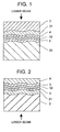
- FIG. 1 illustrates one exemplary construction of a phase change optical recording medium.
- the medium of FIG. 1 includes a reflective layer 5, a second dielectric layer 32, a phase change recording layer 4, a first dielectric layer 31, and a light-transparent substrate 2 stacked successively on a support substrate 20 in the described order.
- a recording/reading beam enters the recording layer 4 through the light-transparent substrate 2.
- the reflective layer 5 is generally constructed of aluminum or an aluminum-base alloy
- the second dielectric layer 32 is generally constructed of ZnS-SiO 2 .
- the reflective layer 5 and/or second dielectric layer 32 in FIG. 1 is preferably formed of a material having a high thermal conductivity. Specifically, it was found preferable that the second dielectric layer 32 is formed of Al 2 O 3 or SiO 2 , and the reflective layer 5 is formed of silver or a silver-base alloy.
- the second dielectric layer 32 is formed of Al 2 O 3 or SiO 2
- the medium somewhat loses storage reliability on account of a likelihood of separation between the second dielectric layer 32 and the recording layer 4 when the medium is stored under hot humid conditions.
- the second dielectric layer 32 is formed of ZnS-SiO 2 and the reflective layer 5 is formed of silver or a silver-base alloy to prevent such separation, the reflective layer 5 can be corroded through reaction of silver in the reflective layer 5 with sulfur (S) in the second dielectric layer 32, which adversely affects recording/reading characteristics.
- An object of the present invention is to provide an optical recording medium having a high storage reliability and satisfactory recording/reading characteristics.
- the inventors sought for the material of which the second dielectric layer 32 is formed that has a higher thermal conductivity than ZnS-SiO 2 , minimizes the likelihood of separation between the second dielectric layer 32 and the recording layer 4, and can prevent corrosion of silver when the reflective layer 5 is formed of silver or a silver-base alloy, and as a result, found that cerium oxide is preferred. It was also found that when at least the region of the first dielectric layer 31 in contact with the recording layer 4 is formed of cerium oxide, the heat dissipation from the recording layer 4 is facilitated and the likelihood of separation between the first dielectric layer 31 and the recording layer 4 is suppressed.
- the likelihood of separation between the mixed dielectric layer and the recording layer 4 is restrained even when stored under hot humid conditions.
- the mixed dielectric layer is disposed in contact with the reflective layer 5 made of silver or a silver-base alloy, it protects the reflective layer 5 from corrosion. Further, the mixed dielectric layer is unlikely to crack during deposition by sputtering.
- the refractive index of the mixed dielectric layer can be controlled over a wide range by altering the mix ratio of cerium oxide to the additive mixture, facilitating the optical design of the medium.
- the minimized likelihood of separation of the mixed dielectric layer from the recording layer is accomplished when the recording layer is made of a metal or alloy.
- the recording layer made of a metal or alloy includes, for example, a phase change recording layer composed mainly of Sb and Te, a phase change recording layer having an approximate composition to Ge 2 Sb 2 Te 5 (atomic ratio), and a magneto-optical recording layer made of a rare earth-transition element alloy. It is noted that there is a strong likelihood of separation between the recording layer and the dielectric layer when thermal impact is applied. Then the present invention is effective especially to phase change media wherein the recording layer can be heated to 200 to 600°C upon initialization (crystallization) or recording.
- FIG. 1 shows one exemplary construction of the optical recording medium of the invention.
- the optical recording medium includes a reflective layer 5, a second dielectric layer 32, a phase change recording layer 4, a first dielectric layer 31, and a light-transparent substrate 2 stacked successively on a support substrate 20 in the described order.
- a recording/reading laser beam enters the recording layer 4 through the light-transparent substrate 2.
- An intermediate layer of dielectric material may be disposed between the support substrate 20 and the reflective layer 5. The construction of each component of this medium is described below.
- the first dielectric layer 31 protects the light-transparent substrate 2 by blocking the heat transferred from the recording layer 4 upon recording or allowing the heat to escape in an in-plane direction.
- the second dielectric layer 32 has the function of cooling the recording layer 4 by allowing the heat transferred from the recording layer 4 upon recording to escape to the reflective layer 5.
- the thicknesses of the first and second dielectric layers 31 and 32 are determined as appropriate so as to provide sufficient cooling, protecting, and modulation improving effects.
- the first dielectric layer 31 preferably has a thickness of 30 to 300 nm, more preferably 50 to 250 nm
- the second dielectric layer 32 preferably has a thickness of 2 to 50 nm. It is noted that the second dielectric layer 32 should preferably have a thickness of not more than 30 nm, more preferably not more than 25 nm, in order to provide a rapid cooling structure.
- At least part of the first dielectric layer 31 and/or at least part of the second dielectric layer 32 is constructed by a mixed dielectric layer containing cerium oxide and an additive compound.
- the molar ratio of the additive compound to the total of cerium oxide and the additive compound is preferably 10 to 80% and more preferably 20 to 60%. If this molar ratio is too low, the addition effect of the additive compound becomes insufficient. On the other hand, too high a molar ratio leads to a likelihood of separation between the mixed dielectric layer and the recording layer 4.
- the mixed dielectric layer should preferably consist of cerium oxide and the additive compound although it may contain at least one of other compounds. Understandably, the total content of the other compounds should preferably be equal to or less than 30 mol% of the entire mixed dielectric layer since too high contents of other compounds may detract from the advantages of the invention. It is preferred to avoid inclusion of sulfides such as ZnS because sulfides can interfere with the advantages of the invention. It is noted that the molar percent is calculated provided that the other compounds are present as compounds having a stoichiometric composition.
- the first dielectric layer 31 in entirety and/or the second dielectric layer 32 in entirety may be constructed by the aforementioned mixed dielectric layer.
- the first dielectric layer 31 and/or the second dielectric layer 32 may be constructed as a structure having at least two dielectric sub-layers stacked, and at least one of the sub-layers is the aforementioned mixed dielectric layer.
- the likelihood of separation between the recording layer 4 and the mixed dielectric layer is suppressed even during storage under hot humid conditions; and as long as the mixed dielectric layer is in contact with the silver-containing reflective layer 5, the likelihood of corrosion of the reflective layer 5 is suppressed.
- Each dielectric layer is preferably formed by a sputtering method.
- the support substrate 20 is provided to maintain the rigidity of the medium.
- the support substrate 20 usually has a thickness of 0.2 to 1.2 mm, preferably 0.4 to 1.2 mm, and may be either transparent or opaque.
- the support substrate 20 may be formed of a resin like conventional optical recording media although it may also be formed of glass. Grooves (or guide channels) often formed in optical recording media can be provided by transferring grooves in the support substrate 20 to the layers formed thereon, as shown in the figure.
- the groove is a region which is relatively on the nearer side as viewed from the recording/reading light incident side, while a land is a region that separates two adjacent grooves.
- the material of which the reflective layer is made is not particularly limited and may be a metal or metalloid such as Al, Au, Ag, Pt, Cu, Ni, Cr, Ti, Si, etc. alone or an alloy containing at least one of the foregoing.
- the dielectric layer-forming material in the invention is selected so as to provide a medium of rapid cooling structure, the reflective layer is preferably formed of a material having a high thermal conductivity compliant to the rapid cooling structure.
- the preferred material having a high thermal conductivity is silver or a silver-base alloy. However, it is preferred to add to silver an element for corrosion resistance improvement since silver in elemental form fails to provide sufficient corrosion resistance.
- the reflective layer on the laser beam-incident side tends to increase surface roughness on account of grain growth during formation of the reflective layer.
- the increased surface roughness leads to increased read noise.
- the reflective layer lowers its thermal conductivity as its grain size becomes smaller. Then, the reflective layer which is amorphous makes it difficult to acquire a sufficient cooling rate upon recording.
- the reflective layer is formed as an amorphous layer, it is crystallized by heat treatment. The layer which is once formed as an amorphous layer and then crystallized maintains the surface roughness inherent to the amorphous state and accomplishes an improvement in thermal conductivity by virtue of crystallization.
- the reflective layer preferably has a thickness of 10 to 300 nm. A thickness below the range is difficult to provide a sufficient reflectance. A thickness beyond the range provides only a little improvement in reflectance and is disadvantageous in cost.
- the reflective layer is preferably formed by vapor phase deposition methods such as sputtering and evaporation.
- the additional element used herein is preferably at least one element selected from among In, Ag, Au, Bi, Se, Al, P, Ge, H, Si, C, V, W, Ta, Zn, Ti, Sn, Pb, Pd and rare earth elements (Sc, Y and lanthanoids). Of these, at least one element selected from among rare earth elements, Ag, In and Ge is more preferred because of their superior storage reliability-improving effect.
- the preferred composition of the recording layer is represented by the formula (I): I (Sb x Te 1-x ) 1-y M y wherein M is an element other than Sb and Te, x and y representative of atomic ratios are preferably in the range: 0.2 ⁇ x ⁇ 0.90, and 0 ⁇ y ⁇ 0.25, and more preferably 0.55 ⁇ x ⁇ 0.85, and 0.01 ⁇ y ⁇ 0.20. Formation of the recording layer from the preferred composition facilitates to increase the data transfer rate.
- the light-transparent substrate 2 is transparent so that recording/reading light is transmitted thereby.
- the light-transparent substrate 2 used herein may be a resin or glass plate having approximately the same thickness as the support substrate 20.
- the present invention is effective especially when high density recording is desired. Therefore, the light-transparent substrate 2 is preferably made thin in order to accomplish a high recording density by way of an increased NA of the recording/reading optical system.
- the thickness of the light-transparent substrate is preferably selected from the range of 30 to 300 ⁇ m. If the light-transparent substrate is too thin, dust deposited on the light-transparent substrate surface has a more detrimental optical influence. On the other hand, if the light-transparent substrate is too thick, it becomes difficult to accomplish a high recording density by way of an increased NA.
- the light-transparent substrate 2 is made thin in various ways.
- a light-transparent sheet of transparent resin may be attached to the first dielectric layer 31 with any of various adhesives and pressure-sensitive adhesives to form a light-transparent substrate.
- a transparent resin layer may be formed directly on the first dielectric layer 31 utilizing a coating technique, to form a light-transparent substrate.
- the light-transparent substrate 2 in FIG. 2 may be of the same material as the support substrate 20 in FIG. 1, but must be transparent to light.
- the protective layer 6 is provided for improving mar resistance and corrosion resistance.
- the protective layer is preferably formed of various organic materials, especially radiation-curable compounds or compositions thereof which are cured with radiation such as electron beams or UV radiation.
- the protective layer usually has a thickness of about 0.1 to 100 ⁇ m and may be formed by conventional techniques such as spin coating, gravure coating, spray coating, and dipping.
- An optical recording disk sample of the structure shown in FIG. 1 was prepared by the following procedure.
- the support substrate 20 used was a disk-shaped polycarbonate having a diameter of 120 mm and a thickness of 1.1 mm in which grooves were formed simultaneous with injection molding.
- the reflective layer 5 was formed in an argon atmosphere by a sputtering process.
- the target used was Ag 98 Pd 1 Cu 1 .
- the reflective layer 5 was 100 nm thick.
- the second dielectric layer 32 was formed in an argon atmosphere by a sputtering process using a composite target of CeO 2 -Al 2 O 3 .
- the second dielectric layer 32 was 12.5 nm thick.
- the recording layer 4 was formed in an argon atmosphere by a sputtering process using an alloy target.
- the recording layer was 12 nm thick.
- the first dielectric layer 31 was formed in an argon atmosphere by a sputtering process using a target of ZnS (80 mol%) and SiO 2 (20 mol%).
- the first dielectric layer 31 was 130 nm thick.
- the light-transparent substrate 2 was formed by bonding a polycarbonate sheet of 100 ⁇ m thick to the surface of the first dielectric layer 31.
- the recording layer of each sample was initialized (or crystallized) by means of a bulk eraser, after which the sample was set on an optical recording medium testing apparatus where signals were recorded under conditions:
- the jitter was a clock jitter which was determined by analyzing read signals by a time interval analyzer to determine "signal fluctuation ( ⁇ )" and computing a value of ⁇ /Tw (%) wherein Tw is a window margin.
- the optimum recording power/optimum erasing power that provided a minimum jitter was determined to be 5.4 mW/2.8 mW for all the samples, at which the jitter was 7.4%. It is seen from these results that all the samples had satisfactory recording/reading characteristics.
- Optical recording disk samples were prepared by the same procedure as sample No. 1 except that the second dielectric layer 32 was formed of CeO 2 -Al 2 O 3 or CeO 2 , the Al 2 O 3 content in the second dielectric layer 32 was changed as shown in Table 1, and the thickness of the second dielectric layer 32 was changed as shown in Table 1. It is noted that the thickness of the second dielectric layer 32 in each sample was set such that the reflectance was identical in all the samples.
- Example 1 For these samples, the optimum recording power Pw which produced a minimum jitter was determined under the same conditions as in Example 1. Also, these samples were stored in a hot humid environment as in Example 1 and examined whether separation occurred between the recording layer 4 and the second dielectric layer 32 after the storage. The results are shown in Table 1. Sample No. Al 2 O 3 (mol%) Thickness (nm) Pw (mW) Separation 4 (comparison) - 8.0 6.0 no 5 10 8.0 6.0 no 6 20 8.5 5.8 no 7 40 9.0 5.7 no 8 60 10.0 5.6 no 9 80 11.0 5.4 occurred
- the second dielectric layer 32 was formed using composite targets containing Cr 2 O 3 , Fe 3 O 4 , Mn 3 O 4 , Nb 2 O 5 , MgO, ZnO, TiO 2 , Y 2 O 3 , Ta 2 O 5 , Sb 2 O 3 , ZrO 2 , Bi 2 O 3 or MgF 2 instead of Al 2 O 3 , the occurrence of cracks in the second dielectric layer 32 was suppressed and no separation of the second dielectric layer 32 was observed. Especially when MgO was used, a crack inhibition effect comparable to the use of Al 2 O 3 , was observed.
- the invention is especially suited for phase change optical recording media and magneto-optical recording media.
Landscapes
- Chemical & Material Sciences (AREA)
- Inorganic Chemistry (AREA)
- Optical Record Carriers And Manufacture Thereof (AREA)
- Thermal Transfer Or Thermal Recording In General (AREA)
Applications Claiming Priority (3)
| Application Number | Priority Date | Filing Date | Title |
|---|---|---|---|
| JP2001357160 | 2001-11-22 | ||
| JP2001357160 | 2001-11-22 | ||
| PCT/JP2002/012223 WO2003044788A1 (fr) | 2001-11-22 | 2002-11-22 | Support d'enregistrement optique |
Publications (1)
| Publication Number | Publication Date |
|---|---|
| EP1447795A1 true EP1447795A1 (fr) | 2004-08-18 |
Family
ID=19168540
Family Applications (1)
| Application Number | Title | Priority Date | Filing Date |
|---|---|---|---|
| EP02788640A Withdrawn EP1447795A1 (fr) | 2001-11-22 | 2002-11-22 | Support d'enregistrement optique |
Country Status (7)
| Country | Link |
|---|---|
| US (1) | US6921568B2 (fr) |
| EP (1) | EP1447795A1 (fr) |
| JP (1) | JP5150999B2 (fr) |
| KR (1) | KR100627036B1 (fr) |
| AU (1) | AU2002355023A1 (fr) |
| TW (1) | TWI249164B (fr) |
| WO (1) | WO2003044788A1 (fr) |
Cited By (2)
| Publication number | Priority date | Publication date | Assignee | Title |
|---|---|---|---|---|
| EP1501091A3 (fr) * | 2003-07-25 | 2008-03-26 | Matsushita Electric Industrial Co., Ltd. | Support d'enregistrement d'informations et son procédé de fabrication |
| EP1726010A4 (fr) * | 2004-03-18 | 2009-03-04 | Ricoh Kk | Support d'enregistrement optique et support d'enregistrement optique bicouche, procede d'enregistrement et de reproduction et appareil d'enregistrement et de reproduction utilisant des supports |
Families Citing this family (9)
| Publication number | Priority date | Publication date | Assignee | Title |
|---|---|---|---|---|
| JP2005302275A (ja) * | 2004-03-18 | 2005-10-27 | Sharp Corp | 光情報記録媒体、記録再生方法、ならびに記録再生装置 |
| DE102004027842A1 (de) * | 2004-06-08 | 2006-01-12 | Institut für Neue Materialien Gemeinnützige GmbH | Abrieb- und kratzfeste Beschichtungen mit niedriger Brechzahl auf einem Substrat |
| CN1922673A (zh) | 2004-11-10 | 2007-02-28 | 松下电器产业株式会社 | 信息记录介质及其制造方法 |
| US20090059758A1 (en) * | 2005-04-07 | 2009-03-05 | Matsushita Electric Industrial Co., Ltd. | Optical information recording medium and method for manufacturing the same |
| US20060228534A1 (en) * | 2005-04-08 | 2006-10-12 | Battelle Memorial Institute | Method for reduction of islanding in metal layers formed on dielectric materials |
| TW200705433A (en) * | 2005-04-13 | 2007-02-01 | Fuji Photo Film Co Ltd | Optical recording medium and method of producing the same |
| JP4612689B2 (ja) * | 2005-12-02 | 2011-01-12 | パナソニック株式会社 | 光学的情報記録媒体とその記録再生方法及び記録再生装置 |
| CN103650120A (zh) * | 2011-07-11 | 2014-03-19 | 松下电器产业株式会社 | 膜结构体及其制造方法 |
| KR20150031380A (ko) * | 2013-09-13 | 2015-03-24 | 삼성전자주식회사 | 캐패시터를 포함하는 반도체 소자 및 그 제조 방법 |
Family Cites Families (22)
| Publication number | Priority date | Publication date | Assignee | Title |
|---|---|---|---|---|
| JPS6251049A (ja) * | 1985-08-29 | 1987-03-05 | Seiko Epson Corp | 光デイスクメモリ |
| JPS6478444A (en) | 1987-09-19 | 1989-03-23 | Nippon Telegraph & Telephone | Rewriting type laser recording medium |
| JPH0192365A (ja) | 1987-10-02 | 1989-04-11 | Shin Nippon Kinzoku Kagaku Kk | 真空蒸着又はスパッタ用酸化セリウム組成物 |
| JPH02239437A (ja) * | 1989-03-13 | 1990-09-21 | Toshiba Corp | 情報記録媒体 |
| JPH0335439A (ja) * | 1989-06-30 | 1991-02-15 | Toshiba Corp | 情報記録媒体 |
| US5368986A (en) * | 1991-05-02 | 1994-11-29 | Hitachi, Ltd. | Information recording media, manufacturing method for the same, and information recording method |
| JPH05144085A (ja) * | 1991-07-15 | 1993-06-11 | Fuji Xerox Co Ltd | 光記録媒体 |
| JPH07262613A (ja) | 1994-03-25 | 1995-10-13 | Toray Ind Inc | 光記録媒体 |
| JPH0863784A (ja) | 1994-06-13 | 1996-03-08 | Matsushita Electric Ind Co Ltd | 光記録媒体及び光記録媒体の使用方法 |
| JP3575274B2 (ja) | 1997-03-27 | 2004-10-13 | 三菱化学株式会社 | 光学的情報記録用媒体 |
| JPH11339314A (ja) * | 1997-07-29 | 1999-12-10 | Toray Ind Inc | 光記録媒体 |
| WO1999013465A1 (fr) * | 1997-09-09 | 1999-03-18 | Hitachi, Ltd. | Support d'enregistrement d'information |
| JPH11238252A (ja) * | 1997-12-18 | 1999-08-31 | Tdk Corp | 光記録媒体 |
| JPH11259912A (ja) * | 1997-12-25 | 1999-09-24 | Tdk Corp | 光記録媒体 |
| JPH11259911A (ja) * | 1997-12-25 | 1999-09-24 | Tdk Corp | 光記録媒体 |
| JP2000067435A (ja) * | 1997-12-27 | 2000-03-03 | Tdk Corp | 光記録媒体およびその記録方法 |
| JPH11232698A (ja) * | 1998-02-17 | 1999-08-27 | Mitsubishi Chemical Corp | 光学的情報記録用媒体及びその製造方法 |
| JP3692776B2 (ja) * | 1998-05-21 | 2005-09-07 | 三菱化学株式会社 | 光学的情報記録用媒体およびその製造方法 |
| JP2000030314A (ja) * | 1998-07-10 | 2000-01-28 | Toray Ind Inc | スパッタリングターゲットおよび光記録媒体の製造方法 |
| US6537721B2 (en) * | 1999-02-15 | 2003-03-25 | Tdk Corporation | Optical recording medium and method for its initialization |
| JP2000331378A (ja) * | 1999-05-19 | 2000-11-30 | Ricoh Co Ltd | 光ディスク |
| JP2002157737A (ja) | 2000-05-12 | 2002-05-31 | Tdk Corp | 光記録方法および光記録媒体 |
-
2002
- 2002-11-21 TW TW091133990A patent/TWI249164B/zh not_active IP Right Cessation
- 2002-11-22 EP EP02788640A patent/EP1447795A1/fr not_active Withdrawn
- 2002-11-22 KR KR1020047007664A patent/KR100627036B1/ko active IP Right Grant
- 2002-11-22 AU AU2002355023A patent/AU2002355023A1/en not_active Abandoned
- 2002-11-22 JP JP2003546341A patent/JP5150999B2/ja not_active Expired - Lifetime
- 2002-11-22 WO PCT/JP2002/012223 patent/WO2003044788A1/fr not_active Application Discontinuation
-
2004
- 2004-04-29 US US10/834,181 patent/US6921568B2/en not_active Expired - Lifetime
Non-Patent Citations (1)
| Title |
|---|
| See references of WO03044788A1 * |
Cited By (3)
| Publication number | Priority date | Publication date | Assignee | Title |
|---|---|---|---|---|
| EP1501091A3 (fr) * | 2003-07-25 | 2008-03-26 | Matsushita Electric Industrial Co., Ltd. | Support d'enregistrement d'informations et son procédé de fabrication |
| EP2296148A1 (fr) * | 2003-07-25 | 2011-03-16 | Panasonic Corporation | Support d'enregistrement d'informations et son procédé de fabrication |
| EP1726010A4 (fr) * | 2004-03-18 | 2009-03-04 | Ricoh Kk | Support d'enregistrement optique et support d'enregistrement optique bicouche, procede d'enregistrement et de reproduction et appareil d'enregistrement et de reproduction utilisant des supports |
Also Published As
| Publication number | Publication date |
|---|---|
| US20040202895A1 (en) | 2004-10-14 |
| KR20040095196A (ko) | 2004-11-12 |
| WO2003044788A1 (fr) | 2003-05-30 |
| JPWO2003044788A1 (ja) | 2005-03-24 |
| JP5150999B2 (ja) | 2013-02-27 |
| TWI249164B (en) | 2006-02-11 |
| TW200300550A (en) | 2003-06-01 |
| AU2002355023A1 (en) | 2003-06-10 |
| KR100627036B1 (ko) | 2006-09-25 |
| US6921568B2 (en) | 2005-07-26 |
Similar Documents
| Publication | Publication Date | Title |
|---|---|---|
| US5498507A (en) | Optical recording media | |
| US5637372A (en) | Phase change optical recording medium | |
| US5523140A (en) | Optical recording method and medium | |
| EP1154413A2 (fr) | Procédé d'enregistrement optique et support | |
| US6329036B1 (en) | Optical recording medium and use | |
| US5637371A (en) | Phase change optical recording medium and activation energy determining method | |
| US6605328B2 (en) | Optical recording medium | |
| EP1385160B1 (fr) | Support d'enregistrement optique à transition de phase | |
| JP3190274B2 (ja) | 光記録媒体およびその製造方法 | |
| US5978349A (en) | Optical recording medium | |
| US6921568B2 (en) | Optical recording medium | |
| US6115351A (en) | Phase change optical recording medium and its writing with high reliability after long period use and/or high environmental temperature storage | |
| US6071587A (en) | Optical recording medium and its recording method | |
| JP4176346B2 (ja) | スパッタターゲットとその製造方法 | |
| EP1197955A2 (fr) | Procédé et support d'enregistrement optique | |
| US20040213121A1 (en) | Optical recording medium and optical recording method | |
| US6192024B1 (en) | Optical recording medium | |
| EP1577888A2 (fr) | Support d'enregistrement optique | |
| JPH11238252A (ja) | 光記録媒体 | |
| EP1281537B1 (fr) | Support d'enregistrement optique | |
| US6706360B2 (en) | Optical recording medium | |
| US6403193B1 (en) | Optical recording medium | |
| US6096400A (en) | Optical recording medium | |
| JPH11167722A (ja) | 光記録媒体、その記録方法およびその記録装置 | |
| US20070104921A1 (en) | Optical recording medium having a higher crystallization speed |
Legal Events
| Date | Code | Title | Description |
|---|---|---|---|
| PUAI | Public reference made under article 153(3) epc to a published international application that has entered the european phase |
Free format text: ORIGINAL CODE: 0009012 |
|
| 17P | Request for examination filed |
Effective date: 20040605 |
|
| AK | Designated contracting states |
Kind code of ref document: A1 Designated state(s): AT BE BG CH CY CZ DE DK EE ES FI FR GB GR IE IT LI LU MC NL PT SE SK TR |
|
| AX | Request for extension of the european patent |
Extension state: AL LT LV MK RO SI |
|
| STAA | Information on the status of an ep patent application or granted ep patent |
Free format text: STATUS: THE APPLICATION HAS BEEN WITHDRAWN |
|
| 18W | Application withdrawn |
Effective date: 20070921 |