EP1443809A2 - Electronic circuit unit and method for manufacturing the same - Google Patents
Electronic circuit unit and method for manufacturing the same Download PDFInfo
- Publication number
- EP1443809A2 EP1443809A2 EP04001625A EP04001625A EP1443809A2 EP 1443809 A2 EP1443809 A2 EP 1443809A2 EP 04001625 A EP04001625 A EP 04001625A EP 04001625 A EP04001625 A EP 04001625A EP 1443809 A2 EP1443809 A2 EP 1443809A2
- Authority
- EP
- European Patent Office
- Prior art keywords
- resin layer
- electronic circuit
- circuit unit
- wiring pattern
- base plate
- Prior art date
- Legal status (The legal status is an assumption and is not a legal conclusion. Google has not performed a legal analysis and makes no representation as to the accuracy of the status listed.)
- Withdrawn
Links
Images

Classifications
-
- H—ELECTRICITY
- H05—ELECTRIC TECHNIQUES NOT OTHERWISE PROVIDED FOR
- H05K—PRINTED CIRCUITS; CASINGS OR CONSTRUCTIONAL DETAILS OF ELECTRIC APPARATUS; MANUFACTURE OF ASSEMBLAGES OF ELECTRICAL COMPONENTS
- H05K1/00—Printed circuits
- H05K1/02—Details
- H05K1/03—Use of materials for the substrate
- H05K1/05—Insulated conductive substrates, e.g. insulated metal substrate
- H05K1/056—Insulated conductive substrates, e.g. insulated metal substrate the metal substrate being covered by an organic insulating layer
-
- H—ELECTRICITY
- H10—SEMICONDUCTOR DEVICES; ELECTRIC SOLID-STATE DEVICES NOT OTHERWISE PROVIDED FOR
- H10W—GENERIC PACKAGES, INTERCONNECTIONS, CONNECTORS OR OTHER CONSTRUCTIONAL DETAILS OF DEVICES COVERED BY CLASS H10
- H10W70/00—Package substrates; Interposers; Redistribution layers [RDL]
- H10W70/60—Insulating or insulated package substrates; Interposers; Redistribution layers
- H10W70/67—Insulating or insulated package substrates; Interposers; Redistribution layers characterised by their insulating layers or insulating parts
- H10W70/68—Shapes or dispositions thereof
- H10W70/6875—Shapes or dispositions thereof being on a metallic substrate, e.g. insulated metal substrates [IMS]
-
- H—ELECTRICITY
- H10—SEMICONDUCTOR DEVICES; ELECTRIC SOLID-STATE DEVICES NOT OTHERWISE PROVIDED FOR
- H10W—GENERIC PACKAGES, INTERCONNECTIONS, CONNECTORS OR OTHER CONSTRUCTIONAL DETAILS OF DEVICES COVERED BY CLASS H10
- H10W90/00—Package configurations
-
- H—ELECTRICITY
- H10—SEMICONDUCTOR DEVICES; ELECTRIC SOLID-STATE DEVICES NOT OTHERWISE PROVIDED FOR
- H10W—GENERIC PACKAGES, INTERCONNECTIONS, CONNECTORS OR OTHER CONSTRUCTIONAL DETAILS OF DEVICES COVERED BY CLASS H10
- H10W72/00—Interconnections or connectors in packages
- H10W72/071—Connecting or disconnecting
- H10W72/075—Connecting or disconnecting of bond wires
-
- H—ELECTRICITY
- H10—SEMICONDUCTOR DEVICES; ELECTRIC SOLID-STATE DEVICES NOT OTHERWISE PROVIDED FOR
- H10W—GENERIC PACKAGES, INTERCONNECTIONS, CONNECTORS OR OTHER CONSTRUCTIONAL DETAILS OF DEVICES COVERED BY CLASS H10
- H10W72/00—Interconnections or connectors in packages
- H10W72/50—Bond wires
- H10W72/551—Materials of bond wires
-
- H—ELECTRICITY
- H10—SEMICONDUCTOR DEVICES; ELECTRIC SOLID-STATE DEVICES NOT OTHERWISE PROVIDED FOR
- H10W—GENERIC PACKAGES, INTERCONNECTIONS, CONNECTORS OR OTHER CONSTRUCTIONAL DETAILS OF DEVICES COVERED BY CLASS H10
- H10W72/00—Interconnections or connectors in packages
- H10W72/90—Bond pads, in general
- H10W72/951—Materials of bond pads
-
- H—ELECTRICITY
- H10—SEMICONDUCTOR DEVICES; ELECTRIC SOLID-STATE DEVICES NOT OTHERWISE PROVIDED FOR
- H10W—GENERIC PACKAGES, INTERCONNECTIONS, CONNECTORS OR OTHER CONSTRUCTIONAL DETAILS OF DEVICES COVERED BY CLASS H10
- H10W90/00—Package configurations
- H10W90/701—Package configurations characterised by the relative positions of pads or connectors relative to package parts
- H10W90/721—Package configurations characterised by the relative positions of pads or connectors relative to package parts of bump connectors
- H10W90/724—Package configurations characterised by the relative positions of pads or connectors relative to package parts of bump connectors between a chip and a stacked insulating package substrate, interposer or RDL
-
- H—ELECTRICITY
- H10—SEMICONDUCTOR DEVICES; ELECTRIC SOLID-STATE DEVICES NOT OTHERWISE PROVIDED FOR
- H10W—GENERIC PACKAGES, INTERCONNECTIONS, CONNECTORS OR OTHER CONSTRUCTIONAL DETAILS OF DEVICES COVERED BY CLASS H10
- H10W90/00—Package configurations
- H10W90/701—Package configurations characterised by the relative positions of pads or connectors relative to package parts
- H10W90/751—Package configurations characterised by the relative positions of pads or connectors relative to package parts of bond wires
- H10W90/754—Package configurations characterised by the relative positions of pads or connectors relative to package parts of bond wires between a chip and a stacked insulating package substrate, interposer or RDL
Definitions
- the present invention relates to an electronic circuit unit suitable for a high-frequency device and a method of manufacturing the same.
- BCB resin benzocyclobutene resin
- a BCB resin layer of a predetermined film thickness is provided on a base plate made of glass or ceramic, and a wiring pattern, an electrode, a resistance film, and the like are provided on a surface of the BCB resin layer (for example, see Japanese Unexamined Patent Application Publication No. 9-55584 (pp. 2 and 3, Fig. 1)).
- a ground conductor layer composed of copper foil between an insulating base plate and a BCB resin layer
- a wiring pattern on a BCB resin plate is formed of a microstrip line, or the wiring pattern and the ground conductor layer are electrically connected to each other via a through-hole provided in the BCB resin layer, thereby forming a ground circuit.
- Circuit elements constituting an electronic circuit are mostly encased within a shield case, but it was impossible to effectively radiate the heat generated from a BCB resin layer to the outside in the conventional electronic circuit unit in which the BCB resin layer is provided on a base plate made of glass or ceramic. That is, since heating elements, such as amplifying transistors, are provided in a high-frequency device, a great deal of heat is radiated from the heating elements in the application of voltage. However, since it is difficult for a BCB resin layer or a base plate made of glass or ceramic to transmit heat, the temperature inside the shield case increases due to the heat generated from the heating elements, creating a situation in which damage could result to other circuit elements.
- an electronic circuit unit used as a high-frequency device is mounted on a motherboard (main board)
- the electronic circuit unit be connected to the ground of an external circuit to enhance the grounding effect.
- the ground conductor layer interposed between the base plate and the BCB resin layer to a ground region on the motherboard side
- an end face electrode had to be previously attached to the electronic circuit unit, or the electronic circuit unit had to be mounted on the motherboard by wire-bonding. Therefore, it was not easy to connect the ground of the external circuit in order to enhance the grounding effect in such a conventional electronic circuit unit.
- the present invention is designed to solve the above-mentioned problems. Accordingly, it is an object of the present invention to provide an electronic circuit unit capable both of effectively radiating the heat generated from a BCB resin layer and of readily connecting with the ground of an external circuit.
- an electronic circuit unit comprises a base plate made of metal, a benzocyclobutene resin layer provided on a surface of the base plate, through-holes provided in the benzocyclobutene resin layer, a wiring pattern provided on a surface of the benzocyclobutene resin layer, and a plurality of circuit elements connected to the wiring pattern.
- circuit elements radiating a great quantity of heat can be directly brought into contact with a base plate made of metal via through-holes in the BCB resin layer, or both of them can be brought into contact with each other by solder within the through-holes, it is possible to effectively radiate heat to the outside by transmitting the heat from the heating elements to the metal base plate.
- circuit elements constituting such an electronic circuit unit include capacitors and resistors, which are formed of a thin film, and bare chip semiconductors, which are wire-bonded to a wiring pattern, it is easy to raise the degree of integration, thereby miniaturization the electric circuit unit.
- the wiring pattern on the BCB resin layer is formed of a microstrip line using the base plate as the ground, it is easy to control the impedance of the wiring pattern when the electronic circuit unit is used as a high-frequency device.
- the ground circuit can be formed in common with the ground of the external circuit only by connecting the base plate to a ground region on the motherboard side, thereby readily improving the grounding effect.
- a method for manufacturing an electronic circuit unit comprises the steps of: forming a benzocyclobutene resin layer on a surface of a base plate made of metal; forming through-holes in the benzocyclobutene resin layer; and forming a wiring pattern on a surface of the benzocyclobutene resin layer.
- the electronic circuit unit manufactured in such a manner can utilize the metal base plate as the ground, there is no need to provide an additional ground conductor layer, thereby reducing the number of required processes.
- the BCB resin layer is formed by a spin coating method, it is possible to equalize the film thickness of the BCB resin layer.
- the BCB resin layer is formed by the spin coating method, it is preferred that the step of forming through-holes by exposing and etching a portion of the BCB resin layer which is formed to a predetermined film thickness be included.
- the BCB resin layer may be formed by a printing method. In this case, cost can be reduced since productivity is improved.
- the wiring pattern of a thin film is formed by a sputtering method, it is possible to perform high-density patterning, thereby miniaturizing the electronic circuit unit.
- the wiring pattern of a thick film may be formed by a printing method, and in that case, cost can be reduced since productivity is improved.
- the present invention is carried out in the above-mentioned manner and has the following advantages.
- circuit elements radiating a great quantity of heat can be brought into contact with the base plate made of metal via the through-holes in the BCB resin layer, it is possible to effectively radiate heat to the outside by transmitting the heat generated from the heating elements to the base plate.
- the ground circuit can be formed in common with the ground of the external circuit only by connecting the base plate to a ground region on the motherboard side, thereby readily improving the grounding effect.
- a method for manufacturing an electronic circuit unit according to the present invention can utilize a metal base plate as the ground, there is no need to provide an additional ground conductor layer, thus reducing the number of required processes. Furthermore, it is easy to equalize film thickness if the BCB resin layer of a thin film is formed by a spin coating method, and it is easy to improve productivity if the BCB resin layer of a thick film is formed by a printing method.
- an electronic circuit unit denoted by reference numeral 1 is used as a high-frequency device and is mounted on a motherboard (main board)(not shown).
- the electronic circuit unit 1 comprises a base plate 2 made of metal, a BCB resin layer 3 of a certain film thickness provided on a surface of the base plate 2, a wiring pattern 4 as a conduction path provided on a surface of the BCB resin layer 3, and a plurality of circuit elements connected to the wiring pattern 4.
- the circuit elements includes a thin film capacitor 5, a thin film resistor 6, bare chip semiconductors 7 and 8, and a flip chip IC 9, and the bare chip semiconductors 7 and 8 are wire-bonded to the wiring pattern 4. Therefore, the electronic circuit of the electronic circuit unit facilitates improvement in the degree of integration, thereby miniaturizing the electric circuit unit.
- the base plate 2 is preferably composed of a plate made of Al or Cu, or a Ni-plate iron plate. Large or small through-holes 3a are provided at predetermined positions on the BCB resin layer 3.
- a ground circuit is formed by electrically connecting the base pattern 4 to the base plate 2 via the through-holes 3a.
- the wiring pattern 4 is mostly formed of the microstrip line using the base plate 2 as the ground.
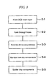
- the above-mentioned electronic circuit unit 1 is fabricated in the following sequence. That is, as shown in Fig. 3, the BCB resin layer 3 of a predetermined thickness is formed by applying and drying BCB resin on a surface of the base plate 2 to a certain film thickness using a spin coating method (S-1). Subsequently, through-holes 3a are formed by exposing and etching portions of the BCB resin layer 3 (S-2). However, the BCB resin layer 3 having the through-holes 3a may be formed by printing and drying BCB resin on a surface of the base plate 2.
- a wiring pattern 4, a thin film capacitor 5, a thin film resistor 6, and the like are formed as a thin film on a surface of the BCB resin layer 3 by a sputtering method (S-3). That is, the wiring pattern 4 and electrodes of the thin film capacitor 5 are formed by sputtering of Cu or Cr followed by etching, a thin film resistor 6 is formed by sputtering of TaSiO 2 followed by etching, and a dielectric film of the thin film capacitor 5 is formed by sputtering of SiO 2 followed by etching.
- the wiring pattern 4, the thin film capacitor 5, and the thin film resistor 6 may be formed as a thick film on a surface of the BCB resin film 3 by a printing method, and the wiring pattern 4, for instance, may be formed by printing and drying Ag paste and the like.
- a plurality of bare chip semiconductors 7 and 8 is die-bonded to the wiring pattern 4 or the base plate 2 via the through-holes 3a, and electrodes on the surfaces of the respective bare chip semiconductors 7 and 8 and the wiring pattern 4 corresponding to the electrodes are then connected to each other by wire bonding (S-4). Furthermore, before and after this process, cream solder is applied on the wiring pattern 4, which is the connection land, and then a variety of chip components including a flip chip IC 9 is mounted thereon. Then, these chip components are soldered by heating in a reflow furnace (S-5).
- a bare chip semiconductor 7 for example, an amplifying transistor
- an amplifying transistor which is a heating element
- it is possible to improve a radiation effect by connecting the heating element to base plate 2 through solder filled within the through-hole 3a of the BCB resin layer 3.
- the wiring pattern 4 is mostly formed of a microstrip line using the base plate 2 as the ground in the electronic circuit unit 1, it is easy to control the impedance of the wiring pattern 4, resulting in facilitation of the design. Furthermore, in the electronic circuit unit 1, since a ground circuit is formed by electrically connecting the wiring pattern 4 to the base plate 2 via the through-holes 3a, the ground circuit can be formed in common with the ground of the external circuit only by connecting the base plate 2 to a ground region on the motherboard side, thereby readily improving the grounding effect.
- the base plate 2 made of metal is utilized as the ground in the electronic circuit unit 1, there is no need to provide an additional ground conductor layer, thereby reducing the number of required processes.
- the employment of a spin coating method as a forming method of the BCB resin layer 3 facilitates obtaining a BCB resin layer 3 of a uniform film thickness
- the employment of a printing method facilitates a reduction in cost since productivity is improved.
- the employment of a sputtering method as a forming method of the wiring pattern 4 facilitates miniaturization since high-density patterning can be performed, and the employment of a printing method facilitates a reduction in cost since productivity is improved.
Landscapes
- Engineering & Computer Science (AREA)
- Microelectronics & Electronic Packaging (AREA)
- Insulated Metal Substrates For Printed Circuits (AREA)
- Parts Printed On Printed Circuit Boards (AREA)
- Structures For Mounting Electric Components On Printed Circuit Boards (AREA)
- Production Of Multi-Layered Print Wiring Board (AREA)
Abstract
Description
Claims (10)
- An electronic circuit unit comprising:a base plate made of metal;a benzocyclobutene resin layer provided on a surface of the base plate;through-holes provided in the benzocyclobutene resin layer;a wiring pattern provided on a surface of the benzocyclobutene resin layer; anda plurality of circuit elements connected to the wiring pattern.
- An electronic circuit unit according to Claim 1,
wherein the plurality of circuit elements comprises a capacitor and a resistor formed of a thin film, and bare chip semiconductors wire-bonded to the wiring pattern. - An electronic circuit unit according to Claim 1 or 2,
wherein the wiring pattern is formed of a microstrip line using the base plate as the ground. - An electronic circuit unit according to any one of Claims 1 to 3,
wherein a ground circuit is formed by electrically connecting the wiring pattern to the base plate via the through-holes. - A method for manufacturing an electronic circuit unit comprising the steps of:forming a benzocyclobutene resin layer on a surface of a base plate made of metal;forming through-holes in the benzocyclobutene resin layer; andforming a wiring pattern on a surface of the benzocyclobutene resin layer.
- A method for manufacturing an electronic circuit unit according to Claim 5,
wherein the benzocyclobutene resin layer is formed by a spin coating method. - A method for manufacturing an electronic circuit unit according to Claim 6,
wherein the through-holes are formed by exposing and etching parts of the benzocyclobutene resin layer. - A method for manufacturing an electronic circuit unit according to Claim 5,
wherein the benzocyclobutene resin layer is formed by a printing method. - A method for manufacturing an electronic circuit unit according to any one of Claims 5 to 8,
wherein the wiring pattern is formed of a thin film by a sputtering method. - A method for manufacturing an electronic circuit unit according to any one of Claims 5 to 8,
wherein the wiring pattern is formed of a thick film by the printing method.
Applications Claiming Priority (2)
| Application Number | Priority Date | Filing Date | Title |
|---|---|---|---|
| JP2003026108 | 2003-02-03 | ||
| JP2003026108A JP2004241416A (en) | 2003-02-03 | 2003-02-03 | Electronic circuit unit and method of manufacturing the same |
Publications (2)
| Publication Number | Publication Date |
|---|---|
| EP1443809A2 true EP1443809A2 (en) | 2004-08-04 |
| EP1443809A3 EP1443809A3 (en) | 2005-11-23 |
Family
ID=32652952
Family Applications (1)
| Application Number | Title | Priority Date | Filing Date |
|---|---|---|---|
| EP04001625A Withdrawn EP1443809A3 (en) | 2003-02-03 | 2004-01-26 | Electronic circuit unit and method for manufacturing the same |
Country Status (2)
| Country | Link |
|---|---|
| EP (1) | EP1443809A3 (en) |
| JP (1) | JP2004241416A (en) |
Cited By (3)
| Publication number | Priority date | Publication date | Assignee | Title |
|---|---|---|---|---|
| US8299692B2 (en) | 2008-04-28 | 2012-10-30 | Samsung Electronics Co., Ltd. | Light emitting device package and method of manufacturing the same |
| WO2013092098A1 (en) * | 2011-12-22 | 2013-06-27 | Siemens Aktiengesellschaft | Circuit carrier with a separate rf circuit and method for populating such a circuit carrier |
| CN112216686A (en) * | 2019-07-09 | 2021-01-12 | 上海华为技术有限公司 | A package structure and power amplifier |
Families Citing this family (1)
| Publication number | Priority date | Publication date | Assignee | Title |
|---|---|---|---|---|
| KR100764388B1 (en) | 2006-03-17 | 2007-10-05 | 삼성전기주식회사 | Anodized Metal Substrate Module |
Family Cites Families (4)
| Publication number | Priority date | Publication date | Assignee | Title |
|---|---|---|---|---|
| KR100223504B1 (en) * | 1992-08-28 | 1999-10-15 | 다카노 야스아키 | Hybrid integrated circuit devices |
| EP0862789A4 (en) * | 1995-11-22 | 1999-07-07 | Olin Corp | SEMICONDUCTOR PACK WITH GROUND OR SUPPLY RING |
| DE19743289C2 (en) * | 1997-09-30 | 2000-02-17 | Siemens Ag | Multi-level intermediate carrier substrate with high wiring density, in particular for multichip modules, and method for its production |
| US20020127494A1 (en) * | 2001-03-08 | 2002-09-12 | Sturni Lance C. | Process for preparing a multi-layer circuit assembly |
-
2003
- 2003-02-03 JP JP2003026108A patent/JP2004241416A/en not_active Withdrawn
-
2004
- 2004-01-26 EP EP04001625A patent/EP1443809A3/en not_active Withdrawn
Cited By (6)
| Publication number | Priority date | Publication date | Assignee | Title |
|---|---|---|---|---|
| US8299692B2 (en) | 2008-04-28 | 2012-10-30 | Samsung Electronics Co., Ltd. | Light emitting device package and method of manufacturing the same |
| US9257615B2 (en) | 2008-04-28 | 2016-02-09 | Samsung Electronics Co., Ltd. | Light emitting device package and method of manufacturing the same |
| WO2013092098A1 (en) * | 2011-12-22 | 2013-06-27 | Siemens Aktiengesellschaft | Circuit carrier with a separate rf circuit and method for populating such a circuit carrier |
| CN112216686A (en) * | 2019-07-09 | 2021-01-12 | 上海华为技术有限公司 | A package structure and power amplifier |
| EP3993574A4 (en) * | 2019-07-09 | 2022-09-21 | Huawei Technologies Co., Ltd. | ENCAPSULATING STRUCTURE AND POWER AMPLIFIER |
| US12341480B2 (en) | 2019-07-09 | 2025-06-24 | Huawei Technologies Co., Ltd. | Packaging structure and power amplifier |
Also Published As
| Publication number | Publication date |
|---|---|
| JP2004241416A (en) | 2004-08-26 |
| EP1443809A3 (en) | 2005-11-23 |
Similar Documents
| Publication | Publication Date | Title |
|---|---|---|
| JP2917868B2 (en) | Semiconductor device and manufacturing method thereof | |
| US6002147A (en) | Hybrid microwave-frequency integrated circuit | |
| JP3235452B2 (en) | High frequency integrated circuit device | |
| JP2988243B2 (en) | Power hybrid integrated circuit device | |
| JPH11191603A (en) | Semiconductor integrated circuit device and method of manufacturing the same | |
| US6357106B1 (en) | Method for mounting parts and making an IC card | |
| US6101098A (en) | Structure and method for mounting an electric part | |
| JPH1022326A (en) | Semiconductor device mounting structure | |
| JP3652102B2 (en) | Electronic circuit module | |
| CN1731915B (en) | multilayer circuit board device | |
| JP3396541B2 (en) | Circuit board mounted with hybrid integrated circuit device | |
| JP2004241416A (en) | Electronic circuit unit and method of manufacturing the same | |
| JPH08250824A (en) | Collinear termination transmission line structure and manufacturing method thereof | |
| US20040055782A1 (en) | Surface-mounting type electronic circuit unit having no melting of solder attaching electric part thereto | |
| JP2541494B2 (en) | Semiconductor device | |
| JP2867737B2 (en) | Hybrid integrated circuit | |
| JP2001068615A (en) | Power amplification module | |
| JPH0746007A (en) | Power board and high frequency power amplifier | |
| JP2556044Y2 (en) | Electronic element mounting board | |
| JPH1022412A (en) | Ball grid array type circuit board | |
| JP3166734B2 (en) | Semiconductor device and method of manufacturing the same | |
| JP2556204B2 (en) | Film carrier semiconductor device mounting method | |
| JP3002857B2 (en) | Bump electrodes and components with bump electrodes | |
| JP2592869Y2 (en) | Hybrid IC device | |
| JP2000216200A (en) | Semiconductor device and its manufacturing method, tape carrier, circuit board, and electronic equipment |
Legal Events
| Date | Code | Title | Description |
|---|---|---|---|
| PUAI | Public reference made under article 153(3) epc to a published international application that has entered the european phase |
Free format text: ORIGINAL CODE: 0009012 |
|
| AK | Designated contracting states |
Kind code of ref document: A2 Designated state(s): AT BE BG CH CY CZ DE DK EE ES FI FR GB GR HU IE IT LI LU MC NL PT RO SE SI SK TR |
|
| AX | Request for extension of the european patent |
Extension state: AL LT LV MK |
|
| PUAL | Search report despatched |
Free format text: ORIGINAL CODE: 0009013 |
|
| AK | Designated contracting states |
Kind code of ref document: A3 Designated state(s): AT BE BG CH CY CZ DE DK EE ES FI FR GB GR HU IE IT LI LU MC NL PT RO SE SI SK TR |
|
| AX | Request for extension of the european patent |
Extension state: AL LT LV MK |
|
| AKX | Designation fees paid | ||
| STAA | Information on the status of an ep patent application or granted ep patent |
Free format text: STATUS: THE APPLICATION IS DEEMED TO BE WITHDRAWN |
|
| 18D | Application deemed to be withdrawn |
Effective date: 20060524 |
|
| REG | Reference to a national code |
Ref country code: DE Ref legal event code: 8566 |