EP1443559B1 - Module d'ensemble de circuits intégrés - Google Patents
Module d'ensemble de circuits intégrés Download PDFInfo
- Publication number
- EP1443559B1 EP1443559B1 EP04250054.6A EP04250054A EP1443559B1 EP 1443559 B1 EP1443559 B1 EP 1443559B1 EP 04250054 A EP04250054 A EP 04250054A EP 1443559 B1 EP1443559 B1 EP 1443559B1
- Authority
- EP
- European Patent Office
- Prior art keywords
- semiconductor die
- wafer
- integrated circuit
- face
- active
- Prior art date
- Legal status (The legal status is an assumption and is not a legal conclusion. Google has not performed a legal analysis and makes no representation as to the accuracy of the status listed.)
- Expired - Lifetime
Links
- 239000004065 semiconductor Substances 0.000 claims description 106
- 235000012431 wafers Nutrition 0.000 claims description 79
- 230000006854 communication Effects 0.000 claims description 24
- 238000004891 communication Methods 0.000 claims description 23
- 229910052751 metal Inorganic materials 0.000 claims description 16
- 239000002184 metal Substances 0.000 claims description 16
- 230000007246 mechanism Effects 0.000 claims description 12
- 238000000034 method Methods 0.000 claims description 11
- OKTJSMMVPCPJKN-UHFFFAOYSA-N Carbon Chemical compound [C] OKTJSMMVPCPJKN-UHFFFAOYSA-N 0.000 claims description 6
- XUIMIQQOPSSXEZ-UHFFFAOYSA-N Silicon Chemical compound [Si] XUIMIQQOPSSXEZ-UHFFFAOYSA-N 0.000 claims description 6
- 239000006260 foam Substances 0.000 claims description 6
- 229910002804 graphite Inorganic materials 0.000 claims description 6
- 239000010439 graphite Substances 0.000 claims description 6
- 229910052710 silicon Inorganic materials 0.000 claims description 6
- 239000010703 silicon Substances 0.000 claims description 6
- 238000001816 cooling Methods 0.000 claims description 4
- 239000007788 liquid Substances 0.000 claims description 3
- 230000003287 optical effect Effects 0.000 claims description 3
- 238000003825 pressing Methods 0.000 claims description 2
- 239000000758 substrate Substances 0.000 description 23
- 230000001070 adhesive effect Effects 0.000 description 5
- 239000000853 adhesive Substances 0.000 description 4
- 230000009286 beneficial effect Effects 0.000 description 3
- 239000004020 conductor Substances 0.000 description 3
- 239000000463 material Substances 0.000 description 3
- 238000005530 etching Methods 0.000 description 2
- 229910052782 aluminium Inorganic materials 0.000 description 1
- XAGFODPZIPBFFR-UHFFFAOYSA-N aluminium Chemical compound [Al] XAGFODPZIPBFFR-UHFFFAOYSA-N 0.000 description 1
- 238000003491 array Methods 0.000 description 1
- 230000008901 benefit Effects 0.000 description 1
- 239000000919 ceramic Substances 0.000 description 1
- 230000008878 coupling Effects 0.000 description 1
- 238000010168 coupling process Methods 0.000 description 1
- 238000005859 coupling reaction Methods 0.000 description 1
- 230000002950 deficient Effects 0.000 description 1
- 230000006870 function Effects 0.000 description 1
- PCHJSUWPFVWCPO-UHFFFAOYSA-N gold Chemical compound [Au] PCHJSUWPFVWCPO-UHFFFAOYSA-N 0.000 description 1
- 229910052737 gold Inorganic materials 0.000 description 1
- 239000010931 gold Substances 0.000 description 1
- 230000010354 integration Effects 0.000 description 1
- 238000004519 manufacturing process Methods 0.000 description 1
- 238000012986 modification Methods 0.000 description 1
- 230000004048 modification Effects 0.000 description 1
- 238000012536 packaging technology Methods 0.000 description 1
- 229920000642 polymer Polymers 0.000 description 1
- 230000008569 process Effects 0.000 description 1
- 230000001105 regulatory effect Effects 0.000 description 1
- XLYOFNOQVPJJNP-UHFFFAOYSA-N water Chemical compound O XLYOFNOQVPJJNP-UHFFFAOYSA-N 0.000 description 1
Images

Classifications
-
- H—ELECTRICITY
- H01—ELECTRIC ELEMENTS
- H01L—SEMICONDUCTOR DEVICES NOT COVERED BY CLASS H10
- H01L23/00—Details of semiconductor or other solid state devices
- H01L23/48—Arrangements for conducting electric current to or from the solid state body in operation, e.g. leads, terminal arrangements ; Selection of materials therefor
-
- H—ELECTRICITY
- H01—ELECTRIC ELEMENTS
- H01L—SEMICONDUCTOR DEVICES NOT COVERED BY CLASS H10
- H01L23/00—Details of semiconductor or other solid state devices
- H01L23/34—Arrangements for cooling, heating, ventilating or temperature compensation ; Temperature sensing arrangements
- H01L23/36—Selection of materials, or shaping, to facilitate cooling or heating, e.g. heatsinks
- H01L23/367—Cooling facilitated by shape of device
-
- H—ELECTRICITY
- H01—ELECTRIC ELEMENTS
- H01L—SEMICONDUCTOR DEVICES NOT COVERED BY CLASS H10
- H01L25/00—Assemblies consisting of a plurality of individual semiconductor or other solid state devices ; Multistep manufacturing processes thereof
- H01L25/03—Assemblies consisting of a plurality of individual semiconductor or other solid state devices ; Multistep manufacturing processes thereof all the devices being of a type provided for in the same subgroup of groups H01L27/00 - H01L33/00, or in a single subclass of H10K, H10N, e.g. assemblies of rectifier diodes
- H01L25/04—Assemblies consisting of a plurality of individual semiconductor or other solid state devices ; Multistep manufacturing processes thereof all the devices being of a type provided for in the same subgroup of groups H01L27/00 - H01L33/00, or in a single subclass of H10K, H10N, e.g. assemblies of rectifier diodes the devices not having separate containers
- H01L25/065—Assemblies consisting of a plurality of individual semiconductor or other solid state devices ; Multistep manufacturing processes thereof all the devices being of a type provided for in the same subgroup of groups H01L27/00 - H01L33/00, or in a single subclass of H10K, H10N, e.g. assemblies of rectifier diodes the devices not having separate containers the devices being of a type provided for in group H01L27/00
- H01L25/0652—Assemblies consisting of a plurality of individual semiconductor or other solid state devices ; Multistep manufacturing processes thereof all the devices being of a type provided for in the same subgroup of groups H01L27/00 - H01L33/00, or in a single subclass of H10K, H10N, e.g. assemblies of rectifier diodes the devices not having separate containers the devices being of a type provided for in group H01L27/00 the devices being arranged next and on each other, i.e. mixed assemblies
-
- H—ELECTRICITY
- H01—ELECTRIC ELEMENTS
- H01L—SEMICONDUCTOR DEVICES NOT COVERED BY CLASS H10
- H01L2225/00—Details relating to assemblies covered by the group H01L25/00 but not provided for in its subgroups
- H01L2225/03—All the devices being of a type provided for in the same subgroup of groups H01L27/00 - H01L33/648 and H10K99/00
- H01L2225/04—All the devices being of a type provided for in the same subgroup of groups H01L27/00 - H01L33/648 and H10K99/00 the devices not having separate containers
- H01L2225/065—All the devices being of a type provided for in the same subgroup of groups H01L27/00 - H01L33/648 and H10K99/00 the devices not having separate containers the devices being of a type provided for in group H01L27/00
- H01L2225/06503—Stacked arrangements of devices
- H01L2225/06513—Bump or bump-like direct electrical connections between devices, e.g. flip-chip connection, solder bumps
-
- H—ELECTRICITY
- H01—ELECTRIC ELEMENTS
- H01L—SEMICONDUCTOR DEVICES NOT COVERED BY CLASS H10
- H01L2225/00—Details relating to assemblies covered by the group H01L25/00 but not provided for in its subgroups
- H01L2225/03—All the devices being of a type provided for in the same subgroup of groups H01L27/00 - H01L33/648 and H10K99/00
- H01L2225/04—All the devices being of a type provided for in the same subgroup of groups H01L27/00 - H01L33/648 and H10K99/00 the devices not having separate containers
- H01L2225/065—All the devices being of a type provided for in the same subgroup of groups H01L27/00 - H01L33/648 and H10K99/00 the devices not having separate containers the devices being of a type provided for in group H01L27/00
- H01L2225/06503—Stacked arrangements of devices
- H01L2225/06527—Special adaptation of electrical connections, e.g. rewiring, engineering changes, pressure contacts, layout
- H01L2225/06531—Non-galvanic coupling, e.g. capacitive coupling
- H01L2225/06534—Optical coupling
-
- H—ELECTRICITY
- H01—ELECTRIC ELEMENTS
- H01L—SEMICONDUCTOR DEVICES NOT COVERED BY CLASS H10
- H01L2225/00—Details relating to assemblies covered by the group H01L25/00 but not provided for in its subgroups
- H01L2225/03—All the devices being of a type provided for in the same subgroup of groups H01L27/00 - H01L33/648 and H10K99/00
- H01L2225/04—All the devices being of a type provided for in the same subgroup of groups H01L27/00 - H01L33/648 and H10K99/00 the devices not having separate containers
- H01L2225/065—All the devices being of a type provided for in the same subgroup of groups H01L27/00 - H01L33/648 and H10K99/00 the devices not having separate containers the devices being of a type provided for in group H01L27/00
- H01L2225/06503—Stacked arrangements of devices
- H01L2225/06589—Thermal management, e.g. cooling
-
- H—ELECTRICITY
- H01—ELECTRIC ELEMENTS
- H01L—SEMICONDUCTOR DEVICES NOT COVERED BY CLASS H10
- H01L23/00—Details of semiconductor or other solid state devices
- H01L23/34—Arrangements for cooling, heating, ventilating or temperature compensation ; Temperature sensing arrangements
- H01L23/46—Arrangements for cooling, heating, ventilating or temperature compensation ; Temperature sensing arrangements involving the transfer of heat by flowing fluids
- H01L23/473—Arrangements for cooling, heating, ventilating or temperature compensation ; Temperature sensing arrangements involving the transfer of heat by flowing fluids by flowing liquids
-
- H—ELECTRICITY
- H01—ELECTRIC ELEMENTS
- H01L—SEMICONDUCTOR DEVICES NOT COVERED BY CLASS H10
- H01L2924/00—Indexing scheme for arrangements or methods for connecting or disconnecting semiconductor or solid-state bodies as covered by H01L24/00
- H01L2924/0001—Technical content checked by a classifier
- H01L2924/0002—Not covered by any one of groups H01L24/00, H01L24/00 and H01L2224/00
Claims (18)
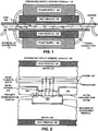
- Module d'assemblage de circuits intégrés (100) supportant une communication capacitive entre puces semi-conductrices, comprenant :une première tranche de silicium (104) avec une face avant et une face arrière à l'opposé de la face avant ;une première couche de puces semi-conductrices, la première couche de puces semi-conductrices comprenant une première puce semi-conductrice (102) avec une face active sur laquelle se trouvent un circuit actif et des plots de signaux, et une face arrière à l'opposé de la face active ;une deuxième couche de puces semi-conductrices, la deuxième couche de puces semi-conductrices comprenant une deuxième puce semi-conductrice (102) avec une face active sur laquelle se trouvent un circuit actif et des plots de signaux, et une face arrière à l'opposé de la face active ;une deuxième tranche de silicium (104) avec une face avant et une face arrière à l'opposé de la face avant ;dans lequel la première puce semi-conductrice et la deuxième puce semi-conductrice sont disposées face active contre face active de telle sorte que les plots de signaux sur la première puce semi-conductrice chevauchent les plots de signaux sur la deuxième puce semi-conductrice pour une communication capacitive entre la première puce semi-conductrice et la deuxième puce semi-conductrice ;dans lequel la première puce semi-conductrice et la deuxième puce semi-conductrice sont pressées ensemble entre la première tranche et la deuxième tranche de telle sorte que la face avant de la première tranche est en contact avec la face arrière de la première puce semi-conductrice et la face avant de la deuxième tranche est en contact avec la face arrière de la deuxième puce semi-conductrice ;dans lequel le module d'assemblage de circuits intégrés comprend en outre une puce semi-conductrice d'entrée/sortie avec une face active sur laquelle se trouvent un circuit actif et des plots de signaux, et une face arrière à l'opposé de la face active ;dans lequel la puce semi-conductrice d'entrée/sortie et la deuxième puce semi-conductrice sont disposées face active contre face active, de telle sorte que les plots de signaux sur la puce semi-conductrice d'entrée/sortie chevauchent les plots de signaux sur la deuxième puce semi-conductrice pour une communication capacitive entre la puce semi-conductrice d'entrée/sortie et la deuxième puce semi-conductrice ;dans lequel la puce semi-conductrice d'entrée/sortie est située sur un bord de la première tranche pour faciliter les communications vers l'intérieur et l'extérieur du module d'assemblage de circuits intégrés ; etdans lequel le bord de la première tranche s'étend au-delà du bord de la deuxième tranche de telle sorte qu'une partie de la face active de la puce semi-conductrice d'entrée/sortie est exposée pour faciliter des connexions externes.
- Module d'assemblage de circuits intégrés de la revendication 1, comprenant en outre :un premier mécanisme d'extraction de chaleur (106) couplé à la face arrière de la première tranche ; etun deuxième mécanisme d'extraction de chaleur (106) couplé à la face arrière de la deuxième tranche.
- Module d'assemblage de circuits intégrés de la revendication 2, dans lequel les premier et deuxième mécanismes d'extraction de chaleur comportent des ailettes de refroidissement pour faciliter le transfert de chaleur à l'air passant à travers les ailettes de refroidissement.
- Module d'assemblage de circuits intégrés de la revendication 2, dans lequel les premier et deuxième mécanismes d'extraction de chaleur comportent de la mousse de graphite ou du métal avec des structures en forme d'ailettes qui facilitent le transfert de chaleur à un liquide pompé à travers la mousse de graphite ou le métal.
- Module d'assemblage de circuits intégrés d'une quelconque revendication précédente, comprenant en outre :une première alimentation électrique (108) couplée à la face arrière de la première tranche ; etune deuxième alimentation électrique (108) couplée à la face arrière de la deuxième tranche.
- Module d'assemblage de circuits intégrés d'une quelconque revendication précédente, dans lequel les première et deuxième tranches comportent des couches métalliques (207) qui alimentent électriquement les première et deuxième puces semi-conductrices.
- Module d'assemblage de circuits intégrés de la revendication 6, dans lequel les première et deuxième tranches comportent des connecteurs d'alimentation sur les faces arrière des première et deuxième tranches.
- Module d'assemblage de circuits intégrés de la revendication 6 ou 7, comprenant en outre des contacts à ressort à système microélectromécanique (MEMS) (210) qui fournissent de l'électricité depuis les couches métalliques à l'intérieur des première et deuxième tranches aux première et deuxième puces semi-conductrices, dans lequel :un premier ensemble de contacts à ressort MEMS sur la face avant de la première tranche touche le côté actif de la deuxième puce semi-conductrice ; etun deuxième ensemble de contacts à ressort MEMS sur la face avant de la deuxième tranche touche le côté actif de la première puce semi-conductrice.
- Module d'assemblage de circuits intégrés de l'une quelconque des revendications 6 à 8, comprenant en outre :un premier régulateur de puissance incorporé à l'intérieur de la première tranche ; etun deuxième régulateur de puissance incorporé à l'intérieur de la deuxième tranche.
- Module d'assemblage de circuits intégrés de la revendication 1, comprenant en outre des plots de connexion optique externe situés sur la partie exposée du côté actif de la puce semi-conductrice d'entrée/sortie.
- Module d'assemblage de circuits intégrés de la revendication 1, comprenant en outre des plots de connexion électrique externe situés sur la partie exposée du côté actif de la puce semi-conductrice d'entrée/sortie.
- Procédé de fabrication d'un module d'assemblage de circuits intégrés (100) comportant des première et deuxième puces semi-conductrices (102) et supportant une communication capacitive entre puces semi-conductrices, chacune des première et deuxième puces semi-conductrices comprenant une face active sur laquelle se trouvent un circuit actif et des plots de signaux, et une face arrière à l'opposé de la face active, le procédé comprenant les étapes suivantes :disposer une première couche de puces semi-conductrices comportant la première puce semi-conductrice et une deuxième couche de puces semi-conductrices comportant la deuxième puce semi-conductrice face active contre face active de telle sorte que les plots de signaux sur la première puce semi-conductrice chevauchent les plots de signaux sur la deuxième puce semi-conductrice pour une communication capacitive entre la première puce semi-conductrice et la deuxième puce semi-conductrice ; etpresser ensemble la première puce semi-conductrice et la deuxième puce semi-conductrice entre une première tranche de silicium (104) et une deuxième tranche de silicium (104) de telle sorte que la première tranche soit en contact avec la face arrière de la première puce semi-conductrice et la deuxième tranche soit en contact avec la face arrière de la deuxième puce semi-conductrice,le module d'assemblage de circuits intégrés comprenant en outre :une puce semi-conductrice d'entrée/sortie avec une face active sur laquelle se trouve un circuit actif - comportant des plots de signaux, et une face arrière à l'opposé de la face active ;dans lequel la puce semi-conductrice d'entrée/ sortie et la deuxième puce semi-conductrice sont disposées face active contre face active de telle sorte que les plots de signaux sur la puce semi-conductrice d'entrée/sortie chevauchent les plots de signaux sur la deuxième puce semi-conductrice, facilitant ainsi une communication capacitive entre la puce semi-conductrice d'entrée/sortie et la deuxième puce semi-conductrice ;dans lequel la puce semi-conductrice d'entrée/ sortie est située sur le bord de la première tranche pour faciliter les communications vers l'intérieur et l'extérieur du module d'assemblage de circuits intégrés ; etdans lequel le bord de la première tranche s'étend au-delà du bord de la deuxième tranche de telle sorte qu'une partie de la face active de la puce semi-conductrice d'entrée/sortie est exposée pour faciliter des connexions externes.
- Procédé de la revendication 12, dans lequel le module d'assemblage de circuits intégrés comprend en outre :un premier mécanisme d'extraction de chaleur (106) couplé au côté de la première tranche à l'opposé de la première puce semi-conductrice ; etun deuxième mécanisme d'extraction de chaleur (106) couplé au côté de la deuxième tranche à l'opposé de la deuxième puce semi-conductrice.
- Procédé de la revendication 12 ou 13, dans lequel le module d'assemblage de circuits intégrés comprend en outre :une première alimentation électrique (108) couplée au côté de la première tranche à l'opposé de la première puce semi-conductrice ; etune deuxième alimentation électrique (108) couplée au côté de la deuxième tranche à l'opposé de la deuxième puce semi-conductrice.
- Procédé de l'une quelconque des revendications 12 à 14, dans lequel les première et deuxième tranches comportent des couches métalliques (207) qui facilitent l'alimentation électrique des première et deuxième puces semi-conductrices.
- Procédé de la revendication 15, dans lequel les première et deuxième tranches comportent des connecteurs d'alimentation sur les côtés des première et deuxième tranches à l'opposé des première et deuxième puces semi-conductrices.
- Procédé de la revendication 15 ou 16, dans lequel le module d'assemblage de circuits intégrés comprend en outre des contacts à ressort à système microélectromécanique (MEMS) (210) qui facilitent la fourniture d'électricité depuis les couches métalliques à l'intérieur des première et deuxième tranches aux première et deuxième puces semi-conductrices, et dans lequel :une première pluralité de contacts à ressort MEMS attachés au côté puce semi-conductrice de la première tranche touche le côté actif de la deuxième puce semi-conductrice ; etune deuxième pluralité de contacts à ressort MEMS attachés au côté puce semi-conductrice de la deuxième tranche touche le côté actif de la première puce semi-conductrice.
- Système informatique comprenant un module d'assemblage de circuits intégrés selon l'une quelconque des revendications 1 à 11.
Applications Claiming Priority (4)
| Application Number | Priority Date | Filing Date | Title |
|---|---|---|---|
| US44380803P | 2003-01-29 | 2003-01-29 | |
| US443808P | 2003-01-29 | ||
| US10/671,642 US6870271B2 (en) | 2003-01-29 | 2003-09-26 | Integrated circuit assembly module that supports capacitive communication between semiconductor dies |
| US671642 | 2003-09-26 |
Publications (3)
| Publication Number | Publication Date |
|---|---|
| EP1443559A2 EP1443559A2 (fr) | 2004-08-04 |
| EP1443559A3 EP1443559A3 (fr) | 2008-07-09 |
| EP1443559B1 true EP1443559B1 (fr) | 2017-05-03 |
Family
ID=32659512
Family Applications (1)
| Application Number | Title | Priority Date | Filing Date |
|---|---|---|---|
| EP04250054.6A Expired - Lifetime EP1443559B1 (fr) | 2003-01-29 | 2004-01-07 | Module d'ensemble de circuits intégrés |
Country Status (4)
| Country | Link |
|---|---|
| US (1) | US6870271B2 (fr) |
| EP (1) | EP1443559B1 (fr) |
| JP (1) | JP4444681B2 (fr) |
| TW (1) | TWI313052B (fr) |
Families Citing this family (28)
| Publication number | Priority date | Publication date | Assignee | Title |
|---|---|---|---|---|
| US7612443B1 (en) | 2003-09-04 | 2009-11-03 | University Of Notre Dame Du Lac | Inter-chip communication |
| US7067910B2 (en) * | 2004-04-13 | 2006-06-27 | Sun Microsystems, Inc. | Method and apparatus for using capacitively coupled communication within stacks of laminated chips |
| US7525199B1 (en) * | 2004-05-21 | 2009-04-28 | Sun Microsystems, Inc | Packaging for proximity communication positioned integrated circuits |
| WO2006011960A1 (fr) * | 2004-06-25 | 2006-02-02 | Sun Microsystems, Inc. | Microcircuit integre soutenant une communication electromagnetique traversant la puce |
| US7175445B2 (en) * | 2004-08-31 | 2007-02-13 | Tyco Electronics Corporation | Electrical connector power wafers |
| US7106079B2 (en) * | 2004-10-22 | 2006-09-12 | Sun Microsystems, Inc. | Using an interposer to facilate capacitive communication between face-to-face chips |
| JP2006190972A (ja) * | 2004-12-08 | 2006-07-20 | Mitsubishi Electric Corp | 電力用半導体装置 |
| EP1701384A1 (fr) * | 2005-03-08 | 2006-09-13 | Sun Microsystems France S.A. | Concept de réseau avec circuits intégrés pour la communication |
| US7573720B1 (en) * | 2005-06-15 | 2009-08-11 | Sun Microsystems, Inc. | Active socket for facilitating proximity communication |
| CA2634756C (fr) * | 2005-12-22 | 2014-07-08 | William Henry Scalia, Jr. | Appareil et procede de controle de debit et temperature de mazout, taille des gouttes de mazout et modulation d'allure de chauffe du bruleur |
| US7356213B1 (en) * | 2006-03-28 | 2008-04-08 | Sun Microsystems, Inc. | Transparent switch using optical and electrical proximity communication |
| US7949436B2 (en) * | 2006-05-19 | 2011-05-24 | Oracle America, Inc. | Method and apparatus for automatically detecting and correcting misalignment of a semiconductor chip |
| US7893531B2 (en) * | 2007-09-28 | 2011-02-22 | Oracle America, Inc. | Integrated-circuit package for proximity communication |
| US8396136B1 (en) | 2009-07-22 | 2013-03-12 | The United States Of America As Represented By The Secretary Of The Navy | Close-proximity communications system using capacitively coupled signal transfer |
| US8164917B2 (en) * | 2009-12-23 | 2012-04-24 | Oracle America, Inc. | Base plate for use in a multi-chip module |
| US8340576B2 (en) * | 2010-06-29 | 2012-12-25 | Stmicroelectronics S.R.L. | Electronic circuit for communicating through capacitive coupling |
| US8150315B2 (en) * | 2010-06-29 | 2012-04-03 | Stmicroelectronics S.R.L. | Method for verifying the alignment between integrated electronic devices |
| US9147636B2 (en) | 2011-06-29 | 2015-09-29 | Stmicroelectronics S.R.L. | Method for verifying the alignment between integrated electronic devices |
| US8704364B2 (en) * | 2012-02-08 | 2014-04-22 | Xilinx, Inc. | Reducing stress in multi-die integrated circuit structures |
| US8704384B2 (en) | 2012-02-17 | 2014-04-22 | Xilinx, Inc. | Stacked die assembly |
| US8957512B2 (en) | 2012-06-19 | 2015-02-17 | Xilinx, Inc. | Oversized interposer |
| US8869088B1 (en) | 2012-06-27 | 2014-10-21 | Xilinx, Inc. | Oversized interposer formed from a multi-pattern region mask |
| US9026872B2 (en) | 2012-08-16 | 2015-05-05 | Xilinx, Inc. | Flexible sized die for use in multi-die integrated circuit |
| US9620473B1 (en) | 2013-01-18 | 2017-04-11 | University Of Notre Dame Du Lac | Quilt packaging system with interdigitated interconnecting nodules for inter-chip alignment |
| US9041220B2 (en) | 2013-02-13 | 2015-05-26 | Qualcomm Incorporated | Semiconductor device having stacked memory elements and method of stacking memory elements on a semiconductor device |
| US9547034B2 (en) | 2013-07-03 | 2017-01-17 | Xilinx, Inc. | Monolithic integrated circuit die having modular die regions stitched together |
| US9915869B1 (en) | 2014-07-01 | 2018-03-13 | Xilinx, Inc. | Single mask set used for interposer fabrication of multiple products |
| US10410950B1 (en) * | 2018-05-11 | 2019-09-10 | Micron Technology, Inc. | Heat spreaders for use with semiconductor devices |
Family Cites Families (11)
| Publication number | Priority date | Publication date | Assignee | Title |
|---|---|---|---|---|
| US4467342A (en) * | 1982-07-15 | 1984-08-21 | Rca Corporation | Multi-chip imager |
| US5491612A (en) * | 1995-02-21 | 1996-02-13 | Fairchild Space And Defense Corporation | Three-dimensional modular assembly of integrated circuits |
| US5567657A (en) * | 1995-12-04 | 1996-10-22 | General Electric Company | Fabrication and structures of two-sided molded circuit modules with flexible interconnect layers |
| JP3937265B2 (ja) * | 1997-09-29 | 2007-06-27 | エルピーダメモリ株式会社 | 半導体装置 |
| SG93192A1 (en) * | 1999-01-28 | 2002-12-17 | United Microelectronics Corp | Face-to-face multi chip package |
| US6559531B1 (en) | 1999-10-14 | 2003-05-06 | Sun Microsystems, Inc. | Face to face chips |
| KR100335717B1 (ko) * | 2000-02-18 | 2002-05-08 | 윤종용 | 고용량 메모리 카드 |
| US6586836B1 (en) * | 2000-03-01 | 2003-07-01 | Intel Corporation | Process for forming microelectronic packages and intermediate structures formed therewith |
| US6507115B2 (en) * | 2000-12-14 | 2003-01-14 | International Business Machines Corporation | Multi-chip integrated circuit module |
| US6495396B1 (en) | 2001-08-29 | 2002-12-17 | Sun Microsystems, Inc. | Method of coupling and aligning semiconductor devices including multi-chip semiconductor devices |
| US6555917B1 (en) * | 2001-10-09 | 2003-04-29 | Amkor Technology, Inc. | Semiconductor package having stacked semiconductor chips and method of making the same |
-
2003
- 2003-09-26 US US10/671,642 patent/US6870271B2/en not_active Expired - Lifetime
-
2004
- 2004-01-07 EP EP04250054.6A patent/EP1443559B1/fr not_active Expired - Lifetime
- 2004-01-28 JP JP2004020598A patent/JP4444681B2/ja not_active Expired - Lifetime
- 2004-01-29 TW TW093102044A patent/TWI313052B/zh not_active IP Right Cessation
Also Published As
| Publication number | Publication date |
|---|---|
| EP1443559A2 (fr) | 2004-08-04 |
| JP2004235644A (ja) | 2004-08-19 |
| EP1443559A3 (fr) | 2008-07-09 |
| US6870271B2 (en) | 2005-03-22 |
| TW200416978A (en) | 2004-09-01 |
| JP4444681B2 (ja) | 2010-03-31 |
| US20040145063A1 (en) | 2004-07-29 |
| TWI313052B (en) | 2009-08-01 |
Similar Documents
| Publication | Publication Date | Title |
|---|---|---|
| EP1443559B1 (fr) | Module d'ensemble de circuits intégrés | |
| TWI527132B (zh) | 晶片封裝,電子計算裝置及用以傳遞信號之方法 | |
| EP2609623B1 (fr) | Communication optique dans un boîtier de puces à empilement en rampe | |
| US5435734A (en) | Direct integrated circuit interconnector system | |
| US20060095639A1 (en) | Structures and methods for proximity communication using bridge chips | |
| US20070210446A1 (en) | Apparatus and Methods For Cooling Semiconductor Integrated Circuit Chip Packages | |
| TWI503948B (zh) | 高頻寬斜堆式晶片封裝 | |
| US7396763B2 (en) | Semiconductor package using flexible film and method of manufacturing the same | |
| US8164917B2 (en) | Base plate for use in a multi-chip module | |
| US7638884B2 (en) | Thin semiconductor device package | |
| WO2009045711A1 (fr) | Caractéristiques d'alignement pour communication de proximité | |
| US8166644B2 (en) | Method for manufacturing an active socket for facilitating proximity communication | |
| US7170121B1 (en) | Computer system architecture using a proximity I/O switch | |
| CN113299632A (zh) | 具有镜像电路的堆叠式晶粒的集成电路器件 | |
| US8026598B2 (en) | Semiconductor chip module with stacked flip-chip unit | |
| JP2000269545A (ja) | 光電子集積回路装置 | |
| KR100225398B1 (ko) | 반도체 범프의 본딩구조 및 방법 | |
| US7659619B1 (en) | Structures for Z-aligned proximity communication | |
| US6958538B1 (en) | Computer system architecture using a proximity I/O switch | |
| CN112151457A (zh) | 封装结构及其制作方法和电子设备 | |
| KR20010025861A (ko) | 적층형 칩 스케일 반도체 패키지 | |
| CN111463187B (zh) | 基于系统级封装的柔性装置及其制造方法 | |
| JP2002110839A (ja) | 半導体装置、半導体装置の製造方法及び半導体実装装置 | |
| CN116033673A (zh) | 电路板级封装方法及电路板 |
Legal Events
| Date | Code | Title | Description |
|---|---|---|---|
| PUAI | Public reference made under article 153(3) epc to a published international application that has entered the european phase |
Free format text: ORIGINAL CODE: 0009012 |
|
| AK | Designated contracting states |
Kind code of ref document: A2 Designated state(s): AT BE BG CH CY CZ DE DK EE ES FI FR GB GR HU IE IT LI LU MC NL PT RO SE SI SK TR |
|
| AX | Request for extension of the european patent |
Extension state: AL LT LV MK |
|
| PUAL | Search report despatched |
Free format text: ORIGINAL CODE: 0009013 |
|
| AK | Designated contracting states |
Kind code of ref document: A3 Designated state(s): AT BE BG CH CY CZ DE DK EE ES FI FR GB GR HU IE IT LI LU MC NL PT RO SE SI SK TR |
|
| AX | Request for extension of the european patent |
Extension state: AL LT LV MK |
|
| 17P | Request for examination filed |
Effective date: 20081009 |
|
| AKX | Designation fees paid |
Designated state(s): DE GB |
|
| RAP1 | Party data changed (applicant data changed or rights of an application transferred) |
Owner name: ORACLE AMERICA, INC. |
|
| 17Q | First examination report despatched |
Effective date: 20110228 |
|
| REG | Reference to a national code |
Ref country code: DE Ref legal event code: R079 Ref document number: 602004051184 Country of ref document: DE Free format text: PREVIOUS MAIN CLASS: H01L0025065000 Ipc: H01L0023367000 |
|
| RIC1 | Information provided on ipc code assigned before grant |
Ipc: H01L 23/367 20060101AFI20160929BHEP Ipc: H01L 23/473 20060101ALN20160929BHEP Ipc: H01L 25/065 20060101ALI20160929BHEP Ipc: H01L 23/48 20060101ALI20160929BHEP |
|
| GRAP | Despatch of communication of intention to grant a patent |
Free format text: ORIGINAL CODE: EPIDOSNIGR1 |
|
| STAA | Information on the status of an ep patent application or granted ep patent |
Free format text: STATUS: GRANT OF PATENT IS INTENDED |
|
| INTG | Intention to grant announced |
Effective date: 20161124 |
|
| GRAS | Grant fee paid |
Free format text: ORIGINAL CODE: EPIDOSNIGR3 |
|
| GRAA | (expected) grant |
Free format text: ORIGINAL CODE: 0009210 |
|
| STAA | Information on the status of an ep patent application or granted ep patent |
Free format text: STATUS: THE PATENT HAS BEEN GRANTED |
|
| AK | Designated contracting states |
Kind code of ref document: B1 Designated state(s): DE GB |
|
| REG | Reference to a national code |
Ref country code: GB Ref legal event code: FG4D |
|
| REG | Reference to a national code |
Ref country code: DE Ref legal event code: R096 Ref document number: 602004051184 Country of ref document: DE |
|
| REG | Reference to a national code |
Ref country code: DE Ref legal event code: R097 Ref document number: 602004051184 Country of ref document: DE |
|
| PLBE | No opposition filed within time limit |
Free format text: ORIGINAL CODE: 0009261 |
|
| STAA | Information on the status of an ep patent application or granted ep patent |
Free format text: STATUS: NO OPPOSITION FILED WITHIN TIME LIMIT |
|
| 26N | No opposition filed |
Effective date: 20180206 |
|
| REG | Reference to a national code |
Ref country code: DE Ref legal event code: R082 Ref document number: 602004051184 Country of ref document: DE Representative=s name: D YOUNG & CO LLP, DE |
|
| PGFP | Annual fee paid to national office [announced via postgrant information from national office to epo] |
Ref country code: GB Payment date: 20221201 Year of fee payment: 20 |
|
| PGFP | Annual fee paid to national office [announced via postgrant information from national office to epo] |
Ref country code: DE Payment date: 20221130 Year of fee payment: 20 |
|
| P01 | Opt-out of the competence of the unified patent court (upc) registered |
Effective date: 20230522 |
|
| REG | Reference to a national code |
Ref country code: DE Ref legal event code: R071 Ref document number: 602004051184 Country of ref document: DE |
|
| REG | Reference to a national code |
Ref country code: GB Ref legal event code: PE20 Expiry date: 20240106 |
|
| PG25 | Lapsed in a contracting state [announced via postgrant information from national office to epo] |
Ref country code: GB Free format text: LAPSE BECAUSE OF EXPIRATION OF PROTECTION Effective date: 20240106 |