EP1441561B1 - Verfahren zur Herstellung und akustischen Verbindung von Strukturen auf einem Substrat - Google Patents
Verfahren zur Herstellung und akustischen Verbindung von Strukturen auf einem Substrat Download PDFInfo
- Publication number
- EP1441561B1 EP1441561B1 EP04380017A EP04380017A EP1441561B1 EP 1441561 B1 EP1441561 B1 EP 1441561B1 EP 04380017 A EP04380017 A EP 04380017A EP 04380017 A EP04380017 A EP 04380017A EP 1441561 B1 EP1441561 B1 EP 1441561B1
- Authority
- EP
- European Patent Office
- Prior art keywords
- mesh
- forming
- chamber
- substrate
- etch
- Prior art date
- Legal status (The legal status is an assumption and is not a legal conclusion. Google has not performed a legal analysis and makes no representation as to the accuracy of the status listed.)
- Expired - Lifetime
Links
- 239000000758 substrate Substances 0.000 title claims abstract description 75
- 238000000034 method Methods 0.000 title claims abstract description 45
- 230000015572 biosynthetic process Effects 0.000 claims description 8
- 238000005530 etching Methods 0.000 claims description 5
- 238000000059 patterning Methods 0.000 claims description 4
- 238000009616 inductively coupled plasma Methods 0.000 abstract description 3
- 230000003247 decreasing effect Effects 0.000 abstract description 2
- 239000002184 metal Substances 0.000 description 15
- 229910052710 silicon Inorganic materials 0.000 description 4
- 239000010703 silicon Substances 0.000 description 4
- XUIMIQQOPSSXEZ-UHFFFAOYSA-N Silicon Chemical compound [Si] XUIMIQQOPSSXEZ-UHFFFAOYSA-N 0.000 description 3
- 239000003989 dielectric material Substances 0.000 description 3
- 238000001459 lithography Methods 0.000 description 3
- 238000004519 manufacturing process Methods 0.000 description 3
- 239000000463 material Substances 0.000 description 3
- 239000003990 capacitor Substances 0.000 description 2
- 238000012805 post-processing Methods 0.000 description 2
- 230000003466 anti-cipated effect Effects 0.000 description 1
- 238000000151 deposition Methods 0.000 description 1
- 239000012528 membrane Substances 0.000 description 1
- 238000012986 modification Methods 0.000 description 1
- 230000004048 modification Effects 0.000 description 1
- 238000012545 processing Methods 0.000 description 1
Images


Classifications
-
- B—PERFORMING OPERATIONS; TRANSPORTING
- B81—MICROSTRUCTURAL TECHNOLOGY
- B81C—PROCESSES OR APPARATUS SPECIALLY ADAPTED FOR THE MANUFACTURE OR TREATMENT OF MICROSTRUCTURAL DEVICES OR SYSTEMS
- B81C1/00—Manufacture or treatment of devices or systems in or on a substrate
- B81C1/00015—Manufacture or treatment of devices or systems in or on a substrate for manufacturing microsystems
- B81C1/00134—Manufacture or treatment of devices or systems in or on a substrate for manufacturing microsystems comprising flexible or deformable structures
- B81C1/00158—Diaphragms, membranes
-
- A—HUMAN NECESSITIES
- A61—MEDICAL OR VETERINARY SCIENCE; HYGIENE
- A61K—PREPARATIONS FOR MEDICAL, DENTAL OR TOILETRY PURPOSES
- A61K8/00—Cosmetics or similar toiletry preparations
- A61K8/02—Cosmetics or similar toiletry preparations characterised by special physical form
- A61K8/0208—Tissues; Wipes; Patches
-
- H—ELECTRICITY
- H04—ELECTRIC COMMUNICATION TECHNIQUE
- H04R—LOUDSPEAKERS, MICROPHONES, GRAMOPHONE PICK-UPS OR LIKE ACOUSTIC ELECTROMECHANICAL TRANSDUCERS; DEAF-AID SETS; PUBLIC ADDRESS SYSTEMS
- H04R19/00—Electrostatic transducers
- H04R19/005—Electrostatic transducers using semiconductor materials
-
- A—HUMAN NECESSITIES
- A61—MEDICAL OR VETERINARY SCIENCE; HYGIENE
- A61K—PREPARATIONS FOR MEDICAL, DENTAL OR TOILETRY PURPOSES
- A61K2800/00—Properties of cosmetic compositions or active ingredients thereof or formulation aids used therein and process related aspects
- A61K2800/20—Chemical, physico-chemical or functional or structural properties of the composition as a whole
- A61K2800/30—Characterized by the absence of a particular group of ingredients
- A61K2800/33—Free of surfactant
-
- A—HUMAN NECESSITIES
- A61—MEDICAL OR VETERINARY SCIENCE; HYGIENE
- A61K—PREPARATIONS FOR MEDICAL, DENTAL OR TOILETRY PURPOSES
- A61K2800/00—Properties of cosmetic compositions or active ingredients thereof or formulation aids used therein and process related aspects
- A61K2800/40—Chemical, physico-chemical or functional or structural properties of particular ingredients
- A61K2800/58—Metal complex; Coordination compounds
-
- A—HUMAN NECESSITIES
- A61—MEDICAL OR VETERINARY SCIENCE; HYGIENE
- A61K—PREPARATIONS FOR MEDICAL, DENTAL OR TOILETRY PURPOSES
- A61K2800/00—Properties of cosmetic compositions or active ingredients thereof or formulation aids used therein and process related aspects
- A61K2800/70—Biological properties of the composition as a whole
- A61K2800/72—Hypo-allergenic
-
- A—HUMAN NECESSITIES
- A61—MEDICAL OR VETERINARY SCIENCE; HYGIENE
- A61K—PREPARATIONS FOR MEDICAL, DENTAL OR TOILETRY PURPOSES
- A61K2800/00—Properties of cosmetic compositions or active ingredients thereof or formulation aids used therein and process related aspects
- A61K2800/74—Biological properties of particular ingredients
- A61K2800/75—Anti-irritant
-
- A—HUMAN NECESSITIES
- A61—MEDICAL OR VETERINARY SCIENCE; HYGIENE
- A61K—PREPARATIONS FOR MEDICAL, DENTAL OR TOILETRY PURPOSES
- A61K2800/00—Properties of cosmetic compositions or active ingredients thereof or formulation aids used therein and process related aspects
- A61K2800/80—Process related aspects concerning the preparation of the cosmetic composition or the storage or application thereof
- A61K2800/94—Involves covalent bonding to the substrate
-
- B—PERFORMING OPERATIONS; TRANSPORTING
- B81—MICROSTRUCTURAL TECHNOLOGY
- B81B—MICROSTRUCTURAL DEVICES OR SYSTEMS, e.g. MICROMECHANICAL DEVICES
- B81B2201/00—Specific applications of microelectromechanical systems
- B81B2201/02—Sensors
- B81B2201/0257—Microphones or microspeakers
Definitions
- the present invention is directed generally to micro-electromechanical Systems (MEMS) devices and, more particularly, to processes for forming chambers and cavities in a substrate and acoustically interconnecting such structures.
- MEMS micro-electromechanical Systems
- Such moving parts typically take the form of a beam or mesh that may form, for example, a variable capacitor, switch, or other component.
- the recent ability to seal micro-machined meshes has lead to the fabrication of microphones and microspeakers. See, for example, International Publication No. WO/01/20948 A2 published 22 March 2001 , entitled MEMS Digital-to-Acoustic Transducer With Error Cancellation.
- a sealed mesh can function as a movable plate of a variable capacitor, and therefore can operate as a microphone.
- the microspeaker needs to be able to push air to create a soundwave just as its larger counterparts must push air to create soundwaves.
- Traditional speaker enclosures have a port on the back to allow the speaker to move freely.
- movement of the sealed mesh inward is inhibited by the inability to compress the air in the chamber while movement of the mesh outward is inhibited by formation of a vacuum. Thus it is necessary to form a vent in the chamber if the microspeaker is to create soundwaves.
- vents are formed by boring through the substrate from the rear. That requires patterning the back side of the substrate followed by an etch through the entirety of the substrate to reach the chamber. Forming of vents by this technique is slow in that several hundred microns of substrate may need to be etched to reach the chamber beneath the sealed mesh and the diameter of the vent is small compared to its depth. Additionally, there are registration problems in that it is necessary to work form the back side of the substrate where there are no landmarks, and hundreds of microns may need to be etched to reach a chamber that may measure in the tens of microns. Thus, the need exists for an easy, repeatable, fast process for forming vents in the chambers of sealed meshes that are to function as speakers.
- the present invention is directed to a process comprising reducing the thickness of a back side of a substrate in an area where vents are to be formed.
- a micro-machined mesh is released from a top side of the substrate.
- a vent opening is formed that connects the released mesh and the area of reduced thickness.
- pilot openings are formed in the substrate in the area of reduced thickness by using at least a portion of the mesh as an etch mask. That assures proper alignment of the vent openings. Releasing of the mesh involves removal of a portion of substrate from beneath the mesh. While the mesh is being released, the vents are formed by expanding the size of the pilot openings.
- the vent openings are formed after the mesh is released.
- the mesh is released using an isotropic etch. After the mesh is released, the mesh is used as an etch mask for an anisotropic etch to form vent openings for connecting the chamber with the area of reduced thickness. Use of the mesh as an etch mask eliminates a lithography step and assures proper alignment of the vent openings.
- vent openings are formed in the area of reduced thickness from the back side of the substrate using an anisotropic etch prior to releasing the mesh.
- the mesh is released using an isotropic etch, during formation of the chamber under the mesh, the chamber intersects the vent openings.
- a common step in the various embodiments of the invention is to reduce the thickness of the substrate in the area of the vent openings. That is accomplished by etching a large cavity; because the diameter of the cavity relative to the depth is large, this step can be carried out efficiently. Connecting to this cavity is accomplished from the top side of the substrate, e.g. by using pilot openings formed using at least a portion of the mesh as an etch mask, by forming the vent openings using the mesh as an etch mask, or by having the chamber intersect the vent openings as the chamber is being formed.
- pilot openings formed using at least a portion of the mesh as an etch mask by forming the vent openings using the mesh as an etch mask, or by having the chamber intersect the vent openings as the chamber is being formed.
- Those embodiments that use the mesh as an etch mask eliminate a lithography step thereby increasing processing speeds.
- FIG. 1 A first embodiment of the present invention is illustrated in conjunction with FIGS. 1-9 .
- a die 10 is received from a CMOS foundry.
- a silicon substrate 12 has been processed so as to form alternating layers of, for example, a dielectric material and a metal.
- the die 10 illustrated in FIG. 1 has a first layer of dielectric material 14 carrying a first metal layer 16.
- the first metal layer 16 has been patterned such that a portion thereof forms a micro-machined mesh 18.
- Formed on the first metal layer 16 is a second layer of dielectric 20.
- the second layer of dielectric 20 carries a second metal layer 22 which has been patterned to have an opening 24 formed therein.
- the second metal layer 22 carries a third layer of dielectric 26.
- the third layer of dielectric 26 carries a third layer of metal 28 which has been patterned to have an opening 30 formed therein.
- a top layer of dielectric 32 is formed on top of the third metal layer 28.
- the present invention is not limited to the position and configuration of the metal layers shown in the figures.
- the pattern shown in FIG. 1 could be implemented in metal layers two, three and four such that references herein to a first, second and third layers of metal need not correspond to metal layers one, two and three, respectively.
- the configuration of the layers of metal need not be as shown in the figures but rather may vary depending upon the device to be fabricated.
- the die 10 would be received, for example, as shown in FIG. 1 from the CMOS foundry. Thereafter, the die 10 will be subjected to post-processing fabrication steps. Although it is anticipated that the post-processing fabrication steps will take place in a facility different from the CMOS foundry which fabricated the die 10, that is not a requirement of the present invention.
- a layer of resist 34 is formed on the back of the substrate 12 and patterned with a mask which is used to form an acoustic cavity.
- the substrate 12 is subjected to an anisotropic etch.
- the anisotropic etch may be a dry, deep reactive ion etch (DRIE) into the substrate 12 to create an acoustic cavity 36. Etching stops at tens to hundreds of microns (dimension h in FIG. 3 ) before the substrate-dielectric interface.
- DRIE deep reactive ion etch
- FIG. 4 illustrates the substrate 12 of FIG. 3 after the resist on the back side of the substrate 12 has been removed and a new layer of resist 38 formed on the top side and patterned to provide an opening 40 in the area of the mesh 18.
- the substrate 12 of FIG. 4 is illustrated being subjected to an anisotropic RIE dry etch through the dielectric layers 32, 26, 20 and 14.
- the patterned resist 38 and the first metal layer 16 are used to pattern the first dielectric layer 14.
- the layer of resist 38 may not be necessary if it is not necessary to protect the top layer of dielectric 32.
- FIG. 6 illustrates the substrate of FIG. 5 after the top side has been patterned with a layer of resist 42 to enable certain portions of the mesh 18 to act as an etch mask for pilot openings to be formed in the substrate 12 in the area of the cavity 36.
- FIG. 7 illustrates the substrate 12 of FIG. 6 being subjected to a DRIE anisotropic etch which forms pilot openings 44 extending through the silicon substrate 12 in the area of the cavity 36.
- FIG. 7A illustrates the same step of the process as FIG. 7 . However, in FIG. 7A it is assumed that the width of the mesh is much smaller (eg..6 microns) then the depth of the reduced substrate (eg. 100 microns). Under these circumstances, formation of the pilot holes 44 may result in formation of vent openings.
- FIGS. 8 and 8A show the substrate 12 of FIGS. 7 and 7A , respectively, after the resist 42 has been removed.
- FIGS. 9 and 9A illustrate the substrate of FIGs. 8 and 8A , respectively, being subjected to an isotropic etch so as to form a chamber 50 under the mesh 18. Forming the chamber 50 releases the mesh 18 from substrate 12.
- the pilot holes 44 are being enlarged to form vent openings 52.
- the already formed vent holes are enlarged.
- the vent openings 52 are formed by enlarging the pilot openings 44, and the pilot openings 44 are formed by using a portion of the mesh 18 as an etch mask, the vent openings 52 will be in alignment so as to connect chamber 50 with cavity 36.
- FIGS. 10 - 15 illustrate another embodiment of the present invention.
- FIG. 10 illustrates the substrate of FIG. 2 after a second layer of resist 54 has been deposited on the back side of the substrate and patterned in a manner, as described below, for forming acoustic cavity 36 and vent openings 52.
- resist 54 a second layer of resist 54 has been deposited on the back side of the substrate and patterned in a manner, as described below, for forming acoustic cavity 36 and vent openings 52.
- FIGs. 11 and 12 illustrate the progression of an anisotropic etch performed on the back side of the substrate 12.
- the etch may be a DRIE and, as the etch progresses, the resist layer 54 is progressively removed. As the layer 54 is progressively removed, vent openings 52 are being formed. Eventually, layer 54 is entirely removed and, as the etch progresses, cavity 36 is formed while the depth of vent openings 52 continues to increase. During this time, a portion of resist layer 34 may be removed as shown in FIG. 12 .
- the etch may be stopped anywhere from a few ten to one hundred microns below the dielectric-silicon interface (h in FIG. 12 ).
- FIG. 13 illustrates the substrate 12 of FIG. 12 after the resist 34 has been removed from the back side of the substrate 12 and the top side has formed thereon a layer of resist 56 having an opening 58 formed therein.
- the opening 58 is designed to expose the mesh 18. Depending upon the need to protect the top layer of dielectric 32, applying and patterning the layer of resist 56 may not be necessary.
- FIG. 14 illustrates the substrate 12 of FIG. 13 after an anisotropic etch of the dielectric material. Additionally, in FIG. 14 , the resist 56 has been removed.
- an isotropic etch of the silicon substrate 12 is performed to remove material from underneath the mesh 18 to thereby release the mesh 18.
- the removal of material from underneath the mesh 18 forms a chamber 50. As the chamber 50 is being formed, it intersects the vent openings 52.
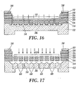
- FIGs. 16 and 17 illustrate another embodiment of the present invention.
- the substrate of FIG. 5 is illustrated.
- an isotropic etch is performed.
- ICP inductively coupled plasma
- the isotropic etch illustrated in FIG. 16 forms a chamber 50 under the mesh 18 thereby releasing the mesh 18.
- an anisotropic etch such as a DRIE etch, is performed using the mesh 18 as an etch mask.
- the anisotropic etch of FIG. 17 forms a plurality of vent openings 60 connecting chamber 50 with acoustic cavity 36.
- the mesh 18 of FIG. 9 , the mesh 18 of FIG. 15 , or the mesh 18 of FIG. 17 may be sealed using known deposition techniques to form a membrane capable of operating as a speaker or a microphone.
- the present invention describes a set of dry etch processes that build an acoustic cavity 36, a chamber 50, and vent openings 52, 60 for acoustically connecting the chamber 50 with the acoustic cavity 36.
- the dry etch processes may use reactive ion etches, which include traditional parallel plate RIE dry etch processes, advanced deep and inductively coupled plasma RIE processes.
- the three embodiments of the present invention illustrate how the present invention may be modified to achieve the result of forming a chamber under a micro-machined mesh, to thereby release the mesh, and acoustically connecting that chamber with an acoustic cavity formed on the back side of the substrate. By forming the cavity on the back side of the substrate, the depth of the vent holes is decreased. Additionally, using the micro-machined mesh as an etch mask for the vent holes makes the process self-aligning.
Landscapes
- Engineering & Computer Science (AREA)
- Health & Medical Sciences (AREA)
- Manufacturing & Machinery (AREA)
- Life Sciences & Earth Sciences (AREA)
- Acoustics & Sound (AREA)
- Signal Processing (AREA)
- Physics & Mathematics (AREA)
- Biomedical Technology (AREA)
- Microelectronics & Electronic Packaging (AREA)
- Birds (AREA)
- Epidemiology (AREA)
- Animal Behavior & Ethology (AREA)
- General Health & Medical Sciences (AREA)
- Public Health (AREA)
- Veterinary Medicine (AREA)
- Micromachines (AREA)
- Electrostatic, Electromagnetic, Magneto- Strictive, And Variable-Resistance Transducers (AREA)
Claims (26)
- Prozess, der umfasst:Reduzieren der Dicke einer Rückseite eines Substrats in einem Bereich, in dem Löcher ausgebildet werden sollen;Ablösen eines Gitters von einer Oberseite des Substrats; undBilden von Lochöffnungen, die das gelöste Gitter und den Bereich mit reduzierter Dicke verbinden.
- Prozess nach Anspruch 1, der außerdem umfasst:Bilden von Pilotöffnungen in dem Substrat in dem Bereich mit reduzierter Dicke unter Verwendung des Gitters als eine Ätzmaske, wobei das Ablösen das Entfernen eines Abschnitts des Substrats unterhalb des Gitters umfasst und wobei das Bilden im Wesentlichen gleichzeitig mit dem Ablösen ausgeführt wird.
- Prozess nach Anspruch 2, der außerdem umfasst:Aufbringen und Strukturieren einer Resistschicht, um bestimmte Abschnitte des Gitters auszuwählen, damit sie als Ätzmaske wirken.
- Prozess nach Anspruch 2, wobei ein anisotropes Ätzen verwendet wird, um die Pilotöffnungen zu bilden, und ein isotropes Ätzen verwendet wird, um das Gitter abzulösen und die Lochöffnungen zu bilden.
- Prozess nach Anspruch 1, wobei das Bilden nach dem Ablösen ausgeführt wird.
- Prozess nach Anspruch 5, wobei das Bilden das Verwenden des Gitters als eine Ätzmaske umfasst.
- Prozess nach Anspruch 6, wobei ein isotropes Ätzen verwendet wird, um das Gitter abzulösen, und ein anisotropes Ätzen für das Bilden verwendet wird.
- Prozess nach Anspruch 1, wobei das Bilden ausgehend von der Rückseite des Substrats vor dem Ablösen ausgeführt wird.
- Prozess nach Anspruch 8, wobei ein anisotropes Ätzen für das Bilden verwendet wird und ein isotropes Ätzen für das Ablösen verwendet wird.
- Prozess nach Anspruch 1, wobei:das Gitter ein mikrobearbeitetes Gitter ist;das Reduzieren der Dicke einen akustischen Hohlraum bildet;das Gitter durch Bilden einer Kammer unter dem Gitter abgelöst wird; unddie Kammer mit dem akustischen Hohlraum akustisch verbunden ist.
- Prozess nach Anspruch 10, der außerdem umfasst:Bilden von Pilotöffnungen in dem Substrat in einem Bereich, in dem sich der akustische Hohlraum befindet, in dem das Gitter als eine Ätzmaske verwendet wird;wobei das Bilden einer Kammer das Entfernen eines Substratanteils von unterhalb des Gitters umfasst und wobei das Verbinden das Verwenden der Pilotöffnungen zum Bilden von Lochöffnungen im Wesentlichen gleichzeitig mit dem Bilden einer Kammer umfasst.
- Prozess nach Anspruch 11, der außerdem umfasst:Aufbringen und Strukturieren einer Resistschicht, um bestimmte Abschnitte des Gitters auszuwählen, damit sie als die Ätzmaske wirken.
- Prozess nach Anspruch 11, wobei ein anisotropes Ätzen verwendet wird, um die Pilotöffnungen zu bilden, und ein isotropes Ätzen verwendet wird, um die Kammer zu bilden und um die Lochöffnungen zu bilden.
- Prozess nach Anspruch 10, wobei das Verbinden nach dem Bilden einer Kammer ausgeführt wird.
- Prozess nach Anspruch 14, wobei das Verbinden das Verwenden des Gitters als eine Ätzmaske zum Bilden von Lochöffnungen umfasst.
- Prozess nach Anspruch 15, wobei ein isotropes Ätzen verwendet wird, um die Kammer zu bilden, und ein anisotropes Ätzen verwendet wird, um die Lochöffnungen zu bilden.
- Prozess nach Anspruch 10, wobei das Verbinden umfasst:Bilden von Lochöffnungen von der Rückseite des Substrats, bevor die Kammer gebildet wird, wobei das Bilden der Kammer das Entfernen eines Substratanteils von unterhalb des Gitters umfasst und wobei das Verbinden umfasst, dass während des Bildens der Kammer die Lochöffnungen mit der Kammer gekreuzt werden.
- Prozess nach Anspruch 17, wobei ein anisotropes Ätzen verwendet wird, um die Lochöffnungen zu bilden, und ein isotropes Ätzen verwendet wird, um die Kammer zu bilden.
- Prozess nach Anspruch 1, wobei:das Gitter ein mikrobearbeitetes Gitter ist und durch Bilden einer Kammer unter dem Gitter abgelöst wird; undim Wesentlichen gleichzeitig mit dem Bilden der Kammer die Kammer mit dem Hohlraum, der durch Reduzierung der Dicke gebildet wird, verbunden wird.
- Prozess nach Anspruch 19, wobei das Verbinden das Bilden von Lochöffnungen zwischen der Kammer und dem Hohlraum umfasst.
- Prozess nach Anspruch 20, wobei das Bilden einer Kammer und das Bilden von Lochöffnungen ein isotropes Ätzen umfassen.
- Prozess nach Anspruch 19, der außerdem umfasst:Bilden von Lochöffnungen von der Rückseite des Substrats im Hohlraum, wobei das Verbinden umfasst, dass während des Bildens der Kammer die Lochöffnungen mit der Kammer gekreuzt werden.
- Prozess nach Anspruch 22, wobei das Bilden einer Kammer und das Verbinden ein isotropes Ätzen umfasst.
- Prozess zum akustischen Verbinden einer Kammer, die unter einem mikrobearbeiteten Gitter gebildet ist, mit einem Hohlraum, der auf der Rückseite eines Substrats gebildet ist, der umfasst:Ätzen von der Oberseite des Substrats, um die Kammer mit dem Hohlraum zu verbinden.
- Prozess nach Anspruch 24, wobei das Ätzen das Bilden von Löchern in dem Substrat in dem Bereich des Hohlraums unter Verwendung des mikrobearbeiteten Gitters als eine Ätzmaske umfasst.
- Prozess nach Anspruch 25, wobei das Ätzen ein anisotropes Ätzen umfasst.
Applications Claiming Priority (2)
| Application Number | Priority Date | Filing Date | Title |
|---|---|---|---|
| US349618 | 2003-01-23 | ||
| US10/349,618 US7049051B2 (en) | 2003-01-23 | 2003-01-23 | Process for forming and acoustically connecting structures on a substrate |
Publications (3)
| Publication Number | Publication Date |
|---|---|
| EP1441561A2 EP1441561A2 (de) | 2004-07-28 |
| EP1441561A3 EP1441561A3 (de) | 2009-06-03 |
| EP1441561B1 true EP1441561B1 (de) | 2011-05-25 |
Family
ID=32594932
Family Applications (1)
| Application Number | Title | Priority Date | Filing Date |
|---|---|---|---|
| EP04380017A Expired - Lifetime EP1441561B1 (de) | 2003-01-23 | 2004-01-22 | Verfahren zur Herstellung und akustischen Verbindung von Strukturen auf einem Substrat |
Country Status (4)
| Country | Link |
|---|---|
| US (1) | US7049051B2 (de) |
| EP (1) | EP1441561B1 (de) |
| JP (1) | JP4672984B2 (de) |
| AT (1) | ATE511320T1 (de) |
Families Citing this family (39)
| Publication number | Priority date | Publication date | Assignee | Title |
|---|---|---|---|---|
| US20050095814A1 (en) * | 2003-11-05 | 2005-05-05 | Xu Zhu | Ultrathin form factor MEMS microphones and microspeakers |
| US7358151B2 (en) | 2004-12-21 | 2008-04-15 | Sony Corporation | Microelectromechanical system microphone fabrication including signal processing circuitry on common substrate |
| DE102005007540A1 (de) | 2005-02-18 | 2006-08-31 | Robert Bosch Gmbh | Mikromechanischer Membransensor mit Doppelmembran |
| US7439093B2 (en) | 2005-09-16 | 2008-10-21 | Dalsa Semiconductor Inc. | Method of making a MEMS device containing a cavity with isotropic etch followed by anisotropic etch |
| US8043950B2 (en) * | 2005-10-26 | 2011-10-25 | Semiconductor Energy Laboratory Co., Ltd. | Semiconductor device and manufacturing method thereof |
| DE102006002106B4 (de) * | 2006-01-17 | 2016-03-03 | Robert Bosch Gmbh | Mikromechanischer Sensor mit perforationsoptimierter Membran sowie ein geeignetes Hestellungsverfahren |
| DE102006022378A1 (de) | 2006-05-12 | 2007-11-22 | Robert Bosch Gmbh | Verfahren zur Herstellung eines mikromechanischen Bauelements und mikromechanisches Bauelement |
| KR20080005854A (ko) * | 2006-07-10 | 2008-01-15 | 야마하 가부시키가이샤 | 압력 센서 및 그의 제조 방법 |
| DE102007019647A1 (de) * | 2007-04-26 | 2008-10-30 | Robert Bosch Gmbh | Verfahren zur Herstellung eines mikromechanischen Bauelements mit Auffüllschicht und Maskenschicht |
| TW200919593A (en) * | 2007-10-18 | 2009-05-01 | Asia Pacific Microsystems Inc | Elements and modules with micro caps and wafer level packaging method thereof |
| EP2218094A1 (de) * | 2007-12-03 | 2010-08-18 | Kolo Technologies, Inc. | Waferdurchgangsverbindungen eines elektrostatischen wandlers und anordnung |
| CN101874343B (zh) * | 2007-12-03 | 2014-09-10 | 科隆科技公司 | 静电换能器阵列的封装和连接 |
| US7795063B2 (en) * | 2007-12-31 | 2010-09-14 | Solid State System Co., Ltd. | Micro-electro-mechanical systems (MEMS) device and process for fabricating the same |
| US8258591B2 (en) * | 2008-01-16 | 2012-09-04 | Solid State System Co., Ltd. | Micro-electro-mechanical systems (MEMS) device |
| US8173471B2 (en) * | 2008-04-29 | 2012-05-08 | Solid State System Co., Ltd. | Method for fabricating micro-electro-mechanical system (MEMS) device |
| TWI380456B (en) | 2008-04-30 | 2012-12-21 | Pixart Imaging Inc | Micro-electro-mechanical device and method for making same |
| CN101580222B (zh) * | 2008-05-15 | 2011-11-16 | 原相科技股份有限公司 | 微机电元件与制作方法 |
| US8144906B2 (en) * | 2008-05-21 | 2012-03-27 | Akustica, Inc. | Wind immune microphone |
| US8345895B2 (en) | 2008-07-25 | 2013-01-01 | United Microelectronics Corp. | Diaphragm of MEMS electroacoustic transducer |
| US8280097B2 (en) * | 2008-08-21 | 2012-10-02 | United Microelectronics Corp. | Microelectromechanical system diaphragm and fabricating method thereof |
| US7951636B2 (en) * | 2008-09-22 | 2011-05-31 | Solid State System Co. Ltd. | Method for fabricating micro-electro-mechanical system (MEMS) device |
| US20100173437A1 (en) * | 2008-10-21 | 2010-07-08 | Wygant Ira O | Method of fabricating CMUTs that generate low-frequency and high-intensity ultrasound |
| TWI484594B (zh) * | 2009-10-07 | 2015-05-11 | United Microelectronics Corp | 具有微機電系統元件之積體電路及其製造方法 |
| US8445324B2 (en) * | 2009-12-16 | 2013-05-21 | Oakland University | Method of wafer-level fabrication of MEMS devices |
| US8030112B2 (en) * | 2010-01-22 | 2011-10-04 | Solid State System Co., Ltd. | Method for fabricating MEMS device |
| US8865500B2 (en) * | 2010-02-03 | 2014-10-21 | United Microelectronics Corp. | Method of fabricating a MEMS microphone with trenches serving as vent pattern |
| TWI430424B (zh) * | 2011-03-18 | 2014-03-11 | Pixart Imaging Inc | 微機電系統聲壓感測元件及其製作方法 |
| CN102752699B (zh) * | 2011-04-19 | 2014-09-17 | 原相科技股份有限公司 | 微机电系统麦克风装置及其制作方法 |
| US8643140B2 (en) | 2011-07-11 | 2014-02-04 | United Microelectronics Corp. | Suspended beam for use in MEMS device |
| US8525354B2 (en) | 2011-10-13 | 2013-09-03 | United Microelectronics Corporation | Bond pad structure and fabricating method thereof |
| CN103347808B (zh) * | 2011-12-29 | 2016-02-10 | 歌尔声学股份有限公司 | 硅基mems麦克风、包含该麦克风的系统和封装 |
| US9402138B2 (en) | 2012-10-12 | 2016-07-26 | Infineon Technologies Ag | MEMS device and method of manufacturing a MEMS device |
| WO2014092541A1 (en) * | 2012-12-10 | 2014-06-19 | Mimos Berhad | A method for releasing mems device |
| US8981501B2 (en) | 2013-04-25 | 2015-03-17 | United Microelectronics Corp. | Semiconductor device and method of forming the same |
| KR102126714B1 (ko) * | 2013-09-03 | 2020-06-26 | 삼성디스플레이 주식회사 | 표시 패널 및 이를 포함하는 유기 발광 표시 장치 |
| US9219185B2 (en) | 2013-12-19 | 2015-12-22 | Excelitas Technologies Singapore Pte. Ltd | CMOS integrated method for the fabrication of thermopile pixel with umbrella absorber on semiconductor substrate |
| US9373772B2 (en) * | 2014-01-15 | 2016-06-21 | Excelitas Technologies Singapore Pte. Ltd. | CMOS integrated method for the release of thermopile pixel on a substrate by using anisotropic and isotropic etching |
| CN106865485B (zh) | 2015-12-10 | 2021-09-21 | 联华电子股份有限公司 | 微机电结构及其制作方法 |
| CN111741423B (zh) * | 2020-08-21 | 2020-11-20 | 中芯集成电路制造(绍兴)有限公司 | Mems麦克风的制造方法 |
Family Cites Families (24)
| Publication number | Priority date | Publication date | Assignee | Title |
|---|---|---|---|---|
| NL8303185A (nl) | 1983-09-15 | 1985-04-01 | Philips Nv | Hybried luidsprekersysteem eventueel met een of meer korrektieketens. |
| JP3172953B2 (ja) * | 1991-08-22 | 2001-06-04 | 株式会社山武 | 静電容量式圧力センサ |
| GB9205711D0 (en) | 1992-03-16 | 1992-04-29 | Lynxvale Ltd | Micromechanical sensor |
| WO1994030030A1 (en) | 1993-06-04 | 1994-12-22 | The Regents Of The University Of California | Microfabricated acoustic source and receiver |
| US5393647A (en) | 1993-07-16 | 1995-02-28 | Armand P. Neukermans | Method of making superhard tips for micro-probe microscopy and field emission |
| US5774252A (en) | 1994-01-07 | 1998-06-30 | Texas Instruments Incorporated | Membrane device with recessed electrodes and method of making |
| US5452268A (en) * | 1994-08-12 | 1995-09-19 | The Charles Stark Draper Laboratory, Inc. | Acoustic transducer with improved low frequency response |
| US5876187A (en) | 1995-03-09 | 1999-03-02 | University Of Washington | Micropumps with fixed valves |
| US5717631A (en) | 1995-07-21 | 1998-02-10 | Carnegie Mellon University | Microelectromechanical structure and process of making same |
| US5949892A (en) | 1995-12-07 | 1999-09-07 | Advanced Micro Devices, Inc. | Method of and apparatus for dynamically controlling operating characteristics of a microphone |
| IL116536A0 (en) | 1995-12-24 | 1996-03-31 | Harunian Dan | Direct integration of sensing mechanisms with single crystal based micro-electric-mechanics systems |
| US5751469A (en) | 1996-02-01 | 1998-05-12 | Lucent Technologies Inc. | Method and apparatus for an improved micromechanical modulator |
| US5936846A (en) * | 1997-01-16 | 1999-08-10 | Ford Global Technologies | Optimized solder joints and lifter pads for improving the solder joint life of surface mount chips |
| DE69731604D1 (de) | 1997-01-31 | 2004-12-23 | St Microelectronics Srl | Herstellungsverfahren für integrierte Halbleitervorrichtung mit einem chemoresistiven Gasmikrosensor |
| US5870482A (en) * | 1997-02-25 | 1999-02-09 | Knowles Electronics, Inc. | Miniature silicon condenser microphone |
| US5867302A (en) | 1997-08-07 | 1999-02-02 | Sandia Corporation | Bistable microelectromechanical actuator |
| US6181050B1 (en) | 1997-10-27 | 2001-01-30 | Hewlett Packard Company | Electrostatic micromotor with large in-plane force and no out-of-plane force |
| EP1105344B1 (de) * | 1998-08-11 | 2012-04-25 | Infineon Technologies AG | Mikromechanischer sensor und verfahren zu seiner herstellung |
| US6255757B1 (en) | 1999-09-01 | 2001-07-03 | Jds Uniphase Inc. | Microactuators including a metal layer on distal portions of an arched beam |
| US6829131B1 (en) * | 1999-09-13 | 2004-12-07 | Carnegie Mellon University | MEMS digital-to-acoustic transducer with error cancellation |
| US6262946B1 (en) | 1999-09-29 | 2001-07-17 | The Board Of Trustees Of The Leland Stanford Junior University | Capacitive micromachined ultrasonic transducer arrays with reduced cross-coupling |
| US6753638B2 (en) * | 2000-02-03 | 2004-06-22 | Calient Networks, Inc. | Electrostatic actuator for micromechanical systems |
| JP3873630B2 (ja) * | 2001-01-29 | 2007-01-24 | セイコーエプソン株式会社 | コンデンサマイクロホンの製造方法 |
| US6943448B2 (en) * | 2003-01-23 | 2005-09-13 | Akustica, Inc. | Multi-metal layer MEMS structure and process for making the same |
-
2003
- 2003-01-23 US US10/349,618 patent/US7049051B2/en not_active Expired - Lifetime
-
2004
- 2004-01-22 EP EP04380017A patent/EP1441561B1/de not_active Expired - Lifetime
- 2004-01-22 AT AT04380017T patent/ATE511320T1/de not_active IP Right Cessation
- 2004-01-23 JP JP2004015101A patent/JP4672984B2/ja not_active Expired - Fee Related
Also Published As
| Publication number | Publication date |
|---|---|
| JP2004223710A (ja) | 2004-08-12 |
| ATE511320T1 (de) | 2011-06-15 |
| US20040146810A1 (en) | 2004-07-29 |
| EP1441561A2 (de) | 2004-07-28 |
| EP1441561A3 (de) | 2009-06-03 |
| JP4672984B2 (ja) | 2011-04-20 |
| US7049051B2 (en) | 2006-05-23 |
Similar Documents
| Publication | Publication Date | Title |
|---|---|---|
| EP1441561B1 (de) | Verfahren zur Herstellung und akustischen Verbindung von Strukturen auf einem Substrat | |
| US6936524B2 (en) | Ultrathin form factor MEMS microphones and microspeakers | |
| EP1529753B1 (de) | Herstellung von sehr dünnen MEMS Mikrophonen und Mikrolautsprechern | |
| US8445324B2 (en) | Method of wafer-level fabrication of MEMS devices | |
| EP1443017B1 (de) | Multimetallschicht MEMS-Struktur und deren Herstellungsverfahren | |
| KR100421217B1 (ko) | 점착 방지 미세 구조물 제조 방법 | |
| WO2009024762A2 (en) | Mems process and device | |
| US10829368B2 (en) | MEMS device and method of manufacturing a MEMS device | |
| KR101601219B1 (ko) | 마이크로폰 및 그 제조 방법 | |
| US7439093B2 (en) | Method of making a MEMS device containing a cavity with isotropic etch followed by anisotropic etch | |
| EP1880977A2 (de) | Silicium auf Metall für MEMS-Vorrichtungen | |
| CN101468784B (zh) | 半导体微型悬浮结构及其制造方法 | |
| GB2452941A (en) | MEMS transducer device and fabrication process | |
| US20070184633A1 (en) | Method of segmenting wafer | |
| US7060522B2 (en) | Membrane structures for micro-devices, micro-devices including same and methods for making same | |
| US9373772B2 (en) | CMOS integrated method for the release of thermopile pixel on a substrate by using anisotropic and isotropic etching | |
| JP2008264951A (ja) | 傾斜形状の加工方法 | |
| US20160039668A1 (en) | Apparatus and method to fabricate mems devce | |
| CN111453694B (zh) | Mems器件及其制造方法 | |
| KR101337568B1 (ko) | 마이크로 그리드 구조체 제조방법 | |
| EP1770057A2 (de) | Verfahren zum Herstellen einer mikroeletrektromechanischen Einrichtung mit einem Diaphragma | |
| WO2014092541A1 (en) | A method for releasing mems device | |
| US20100109121A1 (en) | Microelectromechanical system | |
| KR20030057826A (ko) | 시스템온칩 장치내 미세가공소자의 제조 방법 | |
| CN101200280A (zh) | 制作悬浮结构的方法 |
Legal Events
| Date | Code | Title | Description |
|---|---|---|---|
| PUAI | Public reference made under article 153(3) epc to a published international application that has entered the european phase |
Free format text: ORIGINAL CODE: 0009012 |
|
| AK | Designated contracting states |
Kind code of ref document: A2 Designated state(s): AT BE BG CH CY CZ DE DK EE ES FI FR GB GR HU IE IT LI LU MC NL PT RO SE SI SK TR |
|
| AX | Request for extension of the european patent |
Extension state: AL LT LV MK |
|
| PUAL | Search report despatched |
Free format text: ORIGINAL CODE: 0009013 |
|
| AK | Designated contracting states |
Kind code of ref document: A3 Designated state(s): AT BE BG CH CY CZ DE DK EE ES FI FR GB GR HU IE IT LI LU MC NL PT RO SE SI SK TR |
|
| AX | Request for extension of the european patent |
Extension state: AL LT LV MK |
|
| 17P | Request for examination filed |
Effective date: 20091028 |
|
| AKX | Designation fees paid |
Designated state(s): AT BE BG CH CY CZ DE DK EE ES FI FR GB GR HU IE IT LI LU MC NL PT RO SE SI SK TR |
|
| 17Q | First examination report despatched |
Effective date: 20100519 |
|
| GRAP | Despatch of communication of intention to grant a patent |
Free format text: ORIGINAL CODE: EPIDOSNIGR1 |
|
| GRAS | Grant fee paid |
Free format text: ORIGINAL CODE: EPIDOSNIGR3 |
|
| GRAA | (expected) grant |
Free format text: ORIGINAL CODE: 0009210 |
|
| AK | Designated contracting states |
Kind code of ref document: B1 Designated state(s): AT BE BG CH CY CZ DE DK EE ES FI FR GB GR HU IE IT LI LU MC NL PT RO SE SI SK TR |
|
| REG | Reference to a national code |
Ref country code: GB Ref legal event code: FG4D |
|
| REG | Reference to a national code |
Ref country code: CH Ref legal event code: EP |
|
| REG | Reference to a national code |
Ref country code: IE Ref legal event code: FG4D |
|
| REG | Reference to a national code |
Ref country code: DE Ref legal event code: R096 Ref document number: 602004032789 Country of ref document: DE Effective date: 20110707 |
|
| REG | Reference to a national code |
Ref country code: NL Ref legal event code: VDEP Effective date: 20110525 |
|
| PG25 | Lapsed in a contracting state [announced via postgrant information from national office to epo] |
Ref country code: PT Free format text: LAPSE BECAUSE OF FAILURE TO SUBMIT A TRANSLATION OF THE DESCRIPTION OR TO PAY THE FEE WITHIN THE PRESCRIBED TIME-LIMIT Effective date: 20110926 Ref country code: SE Free format text: LAPSE BECAUSE OF FAILURE TO SUBMIT A TRANSLATION OF THE DESCRIPTION OR TO PAY THE FEE WITHIN THE PRESCRIBED TIME-LIMIT Effective date: 20110525 |
|
| PG25 | Lapsed in a contracting state [announced via postgrant information from national office to epo] |
Ref country code: CY Free format text: LAPSE BECAUSE OF FAILURE TO SUBMIT A TRANSLATION OF THE DESCRIPTION OR TO PAY THE FEE WITHIN THE PRESCRIBED TIME-LIMIT Effective date: 20110525 Ref country code: GR Free format text: LAPSE BECAUSE OF FAILURE TO SUBMIT A TRANSLATION OF THE DESCRIPTION OR TO PAY THE FEE WITHIN THE PRESCRIBED TIME-LIMIT Effective date: 20110826 Ref country code: AT Free format text: LAPSE BECAUSE OF FAILURE TO SUBMIT A TRANSLATION OF THE DESCRIPTION OR TO PAY THE FEE WITHIN THE PRESCRIBED TIME-LIMIT Effective date: 20110525 Ref country code: FI Free format text: LAPSE BECAUSE OF FAILURE TO SUBMIT A TRANSLATION OF THE DESCRIPTION OR TO PAY THE FEE WITHIN THE PRESCRIBED TIME-LIMIT Effective date: 20110525 Ref country code: ES Free format text: LAPSE BECAUSE OF FAILURE TO SUBMIT A TRANSLATION OF THE DESCRIPTION OR TO PAY THE FEE WITHIN THE PRESCRIBED TIME-LIMIT Effective date: 20110905 Ref country code: SI Free format text: LAPSE BECAUSE OF FAILURE TO SUBMIT A TRANSLATION OF THE DESCRIPTION OR TO PAY THE FEE WITHIN THE PRESCRIBED TIME-LIMIT Effective date: 20110525 Ref country code: BE Free format text: LAPSE BECAUSE OF FAILURE TO SUBMIT A TRANSLATION OF THE DESCRIPTION OR TO PAY THE FEE WITHIN THE PRESCRIBED TIME-LIMIT Effective date: 20110525 |
|
| PG25 | Lapsed in a contracting state [announced via postgrant information from national office to epo] |
Ref country code: NL Free format text: LAPSE BECAUSE OF FAILURE TO SUBMIT A TRANSLATION OF THE DESCRIPTION OR TO PAY THE FEE WITHIN THE PRESCRIBED TIME-LIMIT Effective date: 20110525 |
|
| PG25 | Lapsed in a contracting state [announced via postgrant information from national office to epo] |
Ref country code: EE Free format text: LAPSE BECAUSE OF FAILURE TO SUBMIT A TRANSLATION OF THE DESCRIPTION OR TO PAY THE FEE WITHIN THE PRESCRIBED TIME-LIMIT Effective date: 20110525 Ref country code: CZ Free format text: LAPSE BECAUSE OF FAILURE TO SUBMIT A TRANSLATION OF THE DESCRIPTION OR TO PAY THE FEE WITHIN THE PRESCRIBED TIME-LIMIT Effective date: 20110525 |
|
| PG25 | Lapsed in a contracting state [announced via postgrant information from national office to epo] |
Ref country code: RO Free format text: LAPSE BECAUSE OF FAILURE TO SUBMIT A TRANSLATION OF THE DESCRIPTION OR TO PAY THE FEE WITHIN THE PRESCRIBED TIME-LIMIT Effective date: 20110525 Ref country code: DK Free format text: LAPSE BECAUSE OF FAILURE TO SUBMIT A TRANSLATION OF THE DESCRIPTION OR TO PAY THE FEE WITHIN THE PRESCRIBED TIME-LIMIT Effective date: 20110525 Ref country code: SK Free format text: LAPSE BECAUSE OF FAILURE TO SUBMIT A TRANSLATION OF THE DESCRIPTION OR TO PAY THE FEE WITHIN THE PRESCRIBED TIME-LIMIT Effective date: 20110525 |
|
| PLBE | No opposition filed within time limit |
Free format text: ORIGINAL CODE: 0009261 |
|
| STAA | Information on the status of an ep patent application or granted ep patent |
Free format text: STATUS: NO OPPOSITION FILED WITHIN TIME LIMIT |
|
| 26N | No opposition filed |
Effective date: 20120228 |
|
| REG | Reference to a national code |
Ref country code: DE Ref legal event code: R097 Ref document number: 602004032789 Country of ref document: DE Effective date: 20120228 |
|
| PG25 | Lapsed in a contracting state [announced via postgrant information from national office to epo] |
Ref country code: MC Free format text: LAPSE BECAUSE OF NON-PAYMENT OF DUE FEES Effective date: 20120131 |
|
| REG | Reference to a national code |
Ref country code: CH Ref legal event code: PL |
|
| REG | Reference to a national code |
Ref country code: IE Ref legal event code: MM4A |
|
| PG25 | Lapsed in a contracting state [announced via postgrant information from national office to epo] |
Ref country code: CH Free format text: LAPSE BECAUSE OF NON-PAYMENT OF DUE FEES Effective date: 20120131 Ref country code: LI Free format text: LAPSE BECAUSE OF NON-PAYMENT OF DUE FEES Effective date: 20120131 |
|
| PG25 | Lapsed in a contracting state [announced via postgrant information from national office to epo] |
Ref country code: IE Free format text: LAPSE BECAUSE OF NON-PAYMENT OF DUE FEES Effective date: 20120122 |
|
| PG25 | Lapsed in a contracting state [announced via postgrant information from national office to epo] |
Ref country code: BG Free format text: LAPSE BECAUSE OF FAILURE TO SUBMIT A TRANSLATION OF THE DESCRIPTION OR TO PAY THE FEE WITHIN THE PRESCRIBED TIME-LIMIT Effective date: 20110825 |
|
| PG25 | Lapsed in a contracting state [announced via postgrant information from national office to epo] |
Ref country code: TR Free format text: LAPSE BECAUSE OF FAILURE TO SUBMIT A TRANSLATION OF THE DESCRIPTION OR TO PAY THE FEE WITHIN THE PRESCRIBED TIME-LIMIT Effective date: 20110525 |
|
| PG25 | Lapsed in a contracting state [announced via postgrant information from national office to epo] |
Ref country code: LU Free format text: LAPSE BECAUSE OF NON-PAYMENT OF DUE FEES Effective date: 20120122 |
|
| PGFP | Annual fee paid to national office [announced via postgrant information from national office to epo] |
Ref country code: FR Payment date: 20140124 Year of fee payment: 11 |
|
| PG25 | Lapsed in a contracting state [announced via postgrant information from national office to epo] |
Ref country code: HU Free format text: LAPSE BECAUSE OF FAILURE TO SUBMIT A TRANSLATION OF THE DESCRIPTION OR TO PAY THE FEE WITHIN THE PRESCRIBED TIME-LIMIT Effective date: 20040122 |
|
| REG | Reference to a national code |
Ref country code: FR Ref legal event code: ST Effective date: 20150930 |
|
| PG25 | Lapsed in a contracting state [announced via postgrant information from national office to epo] |
Ref country code: FR Free format text: LAPSE BECAUSE OF NON-PAYMENT OF DUE FEES Effective date: 20150202 |
|
| PGFP | Annual fee paid to national office [announced via postgrant information from national office to epo] |
Ref country code: DE Payment date: 20200324 Year of fee payment: 17 Ref country code: IT Payment date: 20200122 Year of fee payment: 17 Ref country code: GB Payment date: 20200127 Year of fee payment: 17 |
|
| REG | Reference to a national code |
Ref country code: DE Ref legal event code: R119 Ref document number: 602004032789 Country of ref document: DE |
|
| GBPC | Gb: european patent ceased through non-payment of renewal fee |
Effective date: 20210122 |
|
| PG25 | Lapsed in a contracting state [announced via postgrant information from national office to epo] |
Ref country code: DE Free format text: LAPSE BECAUSE OF NON-PAYMENT OF DUE FEES Effective date: 20210803 Ref country code: GB Free format text: LAPSE BECAUSE OF NON-PAYMENT OF DUE FEES Effective date: 20210122 |
|
| PG25 | Lapsed in a contracting state [announced via postgrant information from national office to epo] |
Ref country code: IT Free format text: LAPSE BECAUSE OF NON-PAYMENT OF DUE FEES Effective date: 20210122 |