FIELD OF THE INVENTION
The present invention relates to display devices, such as
organic electroluminescence display devices, which have a
display panel comprising a plurality of pixels arranged in the
form of a matrix.
BACKGROUND OF THE INVENTION
Progress has been made in recent years in developing
organic electroluminescence displays (hereinafter referred to
as "organic EL displays"). Use of organic EL displays, for
example, in portable telephones is under study. The methods
of driving organic EL display already known are the passive
matrix drive method wherein scanning electrodes and data
electrodes are used for time division driving, and the active
matrix drive method wherein each pixel is held luminescent for
one vertical scanning period.
With organic EL displays of the active matrix drive type,
each pixel 52 has as shown in FIG. 51 an organic EL element 50,
a drive transistor TR2 for controlling the energization of the
EL element 50, a write transistor TR1 which is brought into
conduction upon application of scanning voltage SCAN by a
scanning electrode, and a capacitance element C to which data
voltage DATA is applied from a data electrode by the
conduction of the write transistor TR1. The output voltage of
the capacitance element C is applied to the gate of the drive
transistor TR2.
First, voltage is applied to scanning electrodes one
after another to cause a plurality of write transistors TR1
connected to the same scanning electrode to conduct, and data
voltage (input signal) is applied to data electrodes in
synchronism with the scanning. Since the write transistor TR1
is in conduction at this time, a charge corresponding to the
data voltage is stored in the capacitance element C. The
operating state of the drive transistor TR2 is dependent on
the quantity of charge stored in the capacitance element C.
When the drive transistor TR2 is brought into conduction, a
value of current corresponding to the data voltage is supplied
to the EL element 50 via the drive transistor TR2.
Consequently, the EL element 50 luminesces with brightness
corresponding to the data voltage. The element 50 is held
thus luminescent during one vertical scanning period.
The problem of display irregularities is encountered
with organic EL displays of the analog drive type wherein a
value of current corresponding to the data voltage is supplied
to the organic EL element 50 to cause the luminescence of the
EL element 50 with brightness in proportion to the data
voltage. Accordingly, an organic EL display of the digital
drive type has been proposed in which pulse current having a
duty ratio in accordance with data voltage is supplied to the
organic EL element 50 to thereby realize multi-level gradation
(see, for example, JP-A No. 1998-312173).
With the organic EL display of the digital drive type, 1
field (or 1 frame) which is the display period of a screen of
data or image is divided into a plurality of (N) subfields (or
subframes) SF, and each subfield SF comprises a scanning
period and a luminescence period as shown in FIG. 53 (a). The
scanning periods included in one field are all equal in length,
but the luminescence periods have varying lengths of nth power
of 2 (n = 0, 1, 2, ... N-1.). In the illustrated case (N = 4),
four luminescence periods are given respective lengths of 8, 4,
2, 1, and on/off changes of the luminescence periods realize
expression of 16-level gradation.
In each subfield SF of the subfield drive method
described, scanning voltage is applied during the scanning
period to the write transistor TR1 constituting each pixel to
write binary data of the subfield to the capacitance element C,
and current corresponding to the binary data is supplied to
the EL element by the drive transistor TR2 during the
subsequent luminescence period.
However, in the organic EL display using the subfield
drive method described, all the horizontal scanning lines must
be scanned in each of the subfields within one field, so that
there arise the problem that multi-level gradation requires
high-speed scanning, and the problem that quasi-contours will
occur.
The present applicant has therefore proposed an organic
EL display device shown in FIG. 52. This EL display device
has pixels 51 each comprising an organic EL element 50, a
drive transistor TR2 for energizing or deenergizing the EL
element 50 in response to an on/off control signal input to
the gate thereof, a write transistor TR1 brought into
conduction when scanning voltage is applied to the gate
thereof by a scanning driver, a capacitance element C to which
data voltage is applied from a data driver by the conduction
of the write transistor TR1, and a comparator 9 having a pair
of positive and negative input terminals to be supplied with
ramp voltage from a ramp voltage generating circuit and output
voltage from the capacitance element C for comparing the two
voltages. The comparator 9 feeds an output signal to the gate
of the drive transistor TR2.
A current supply line 54 is connected to the source of
the drive transistor TR2, and the EL element 50 is connected
to the drain of the drive transistor TR2. The data driver is
connected to one electrode (e.g., source) of the write
transistor TR1, and the other electrode (e.g., drain) of the
write transistor TR1 has connected thereto one end of the
capacitance element C and the inversion input terminal of the
comparator 9. The output terminal of the ramp voltage
generating circuit is connected to the noninversion input
terminal of the comparator 9.
With the organic EL display device described above, one
field period is divided into a first half, i.e., a scanning
period, and a second half, i.e., a luminescence period as
shown in FIG. 53 (b). During the scanning period, scanning
voltage is applied, for each horizontal line, from the
scanning driver to the write transistor TR1 constituting each
pixel 51 to bring the transistor TR1 into conduction, whereby
data voltage is applied from the data driver to the
capacitance element C and stored therein as a charge.
Consequently, data for one field is set in all the pixels
constituting the EL display device.
The ramp voltage generating circuit produces a ramp
voltage which is held at a high value during the scanning
period in the first half of every field period and which
varies linearly from a low value to a high value during the
luminescence period in the second half of the field period as
shown in FIG. 53 (c). During the first-half scanning period,
the circuit applies a high voltage to the noninversion input
terminal of the comparator 9. This always causes the
comparator 9 to produce a high output as shown in FIG. 53 (d)
irrespective of the input voltage to the inversion input
terminal.
When the ramp voltage is applied from the ramp voltage
generating circuit to the noninversion input terminal of the
comparator 9 during the second-half luminescence period, the
output voltage (data voltage) of the capacitance element C is
applied to the inversion input terminal of the comparator 9 at
the same time, with the result that the output of the
comparator 9 is given low and high two values in accordance
with the result of comparison between the two voltages as
shown in FIG. 53 (d). Stated more specifically, the
comparator produces a low output while the ramp voltage is
lower than the data voltage and produces a high output while
the ramp voltage is higher than the data voltage. The length
of the period during which the comparator output is low is in
proportion to the magnitude of the data voltage.
In this way, the output of the comparator 9 becomes low
only during a period in proportion to the magnitude of the
data voltage, whereby the drive transistor TR2 is brought into
conduction only during this period to energize the EL element
50. As a result, the EL element 50 of each pixel 51
luminesces only during the period in proportion to the
magnitude of the data voltage for the pixel 51 within one
field period, whereby expression of multi-level gradation is
realized.
The organic EL display device described does not require
high-speed scanning since multi-level gradation can be
expressed by scanning once during one field period, and is
free of the likelihood of producing quasi-contours. With the
organic EL device comprising the pixel 51 shown in FIG. 52,
however, there is the likelihood that the characteristics of
transistors constituting the comparator 9 inevitably involve
variations, with the result that the period during which the
output of the comparator 9 is low, namely, the period of time
during which current flows through the EL element 50, becomes
no longer accurately proportional to the magnitude of the data
voltage. Thus, the problem that display irregularities occur
to result in an impaired image quality still remains to be
solved. With the display device disclosed in JP-B No. 3305946
or JP-A No. 2002-297097, the current flowing through the
comparator becomes too great to be negligible as compared with
the current flowing through the EL element, hence the problem
of increased power consumption.
SUMMARY OF THE INVENTION
A first object of the present invention is to provide a
display device of the active matrix drive type wherein the
duration of energization of the display element is accurately
in proportion to the value of data voltage despite variations
in the characteristics of transistors constituting the pixel
of the device.
A second object of the invention is to provide a display
device of the active matrix drive type which is diminished in
power consumption as compared with devices of the prior art.
The present invention provides a display device of the
active matrix drive type comprising a display panel having a
plurality of pixels arranged in the form of a matrix, each of
the pixels of the display panel having a display element
luminescent when supplied with electric power, and a control
circuit for controlling the luminescence period of the display
element within 1 frame period in accordance with data voltage
to be supplied from outside. The control circuit of each
pixel of the display panel comprises a first control element
for starting to energize the display element and a second
control element for deenergizing the display element.
With the display device of the present invention, each
pixel of the display panel has therein a first control element
for starting to energize the display element and a second
control element for deenergizing the display element. In
fabricating the display panel, therefore, the two control
elements in the same pixel are produced at the same time as
positioned in close proximity to each other by the same
process. Accordingly, these two control elements involve
similar variations in characteristics, such that even if the
time for the first control element to operate to start the
energization of the display element differs, the time for the
second control element to operate to deenergize the display
element also differs to the same extent in the same direction.
It therefore follows that the duration of energization of the
display element is a length of time in accordance with the
data voltage despite the variations involved in the
characteristics of the two control elements.
The present invention further provides a display device
of the active matrix drive type comprising a display panel
having a plurality of pixels arranged in the form of a matrix,
and a scanning driver and a data driver which are connected to
the display panel. Each of the pixels of the display panel
comprises:
Stated more specifically, the on-control element
operates when impressed with a voltage in accordance with the
ramp voltage to turn on the drive element, and the off-control
element operates when impressed with a voltage in accordance
with the sum of the data voltage and the ramp voltage to turn
off the drive element. Alternatively, the on-control element
operates when impressed with a voltage in accordance with the
value of sum of the data voltage and the ramp voltage to turn
on the drive element, and the off-control element operates
when impressed with a voltage in accordance with the value of
the ramp voltage to turn off the drive element.
With the display device of the active matrix drive type
according to the present invention, the write element of each
pixel is impressed with scanning voltage from the scanning
driver during the scanning period within 1 frame period and
thereby brought into conduction, whereby data voltage is
applied to the voltage holding means from the data driver and
held in the holding means. During the luminescence period
within 1 frame period, on the other hand, ramp voltage having
a predetermined rate of variation is applied to the pulse-width
modulation control means, which pulse-width-modulates
the output voltage (data voltage) of the voltage holding means
with the ramp voltage, and the on-control element turns on the
drive element according to the result. Upon lapse of a period
in proportion to the data voltage, the off-control element
turns off the drive element. Consequently, the display
element is energized only during a period in proportion to the
data voltage.
The pair of on-control element and off-control element
are positioned in close proximity to each other within the
same pixel and are produced by the same process at the same
time. Accordingly, these two control elements involve similar
variations in characteristics (e.g., in gate-source threshold
level), such that even if the time for the on-control element
to turn on the drive element differs due to the variation, the
time for the off-control element to turn off the drive element
thereafter also differs to the same extent in the same
direction. It therefore follows that the period of from the
time the drive element is turned on by the on-control element
until the time the drive element is turned off by the off-control
element is a length of time in accordance with the
data voltage despite the variations involved in the
characteristics of the two control elements.
With the display device of the active matrix drive type
according to the invention, each pixel of the display panel
has a first control element for starting to energize the
display element, and a second control element for deenergizing
the display element. States more specifically, when the first
control element also serves to drive the display element, the
first control element is provided on and connected in series
with a power supply line extending from a power source for
supplying electric power to the display element, is turned on
when starting to energize the display element and starts to
energize the display element. The second control element is
turned on when deenergizing the display element and turns off
the first control element to thereby deenergize the display
element.
In the case where the first control element and the
second control element comprise a first transistor and a
second transistor, respectively, the first transistor serves
as a drive transistor for driving the display element.
Accordingly, the first transistor can be made to operate in
either one of the linear region (nonsaturation region) and the
saturation region by altering the cathode potential of the
display element. When the drive transistor is operated in the
saturation region, variations in the characteristics of the
drive transistor exert a great influence on the duration of
energization of the display element, whereas if the drive
transistor comprises the first transistor, the first
transistor and the second transistor for controlling the
duration of energization of the display element each have the
characteristics variations offset by those of the other. The
first transistor can therefore be made to operate not only in
the linear region but also in the saturation region.
The first control element, which is provided on and
positioned in series with the power supply line extending from
a power source for supplying electric power to the display
element, on/off-controls the energization of the display
element, so that the current from the power source flows only
through the power supply line for energization. Flow of
useless current is thus avoidable.
With the display device of the active matrix drive type
according to the invention, the control circuit of each pixel
has a first control element for starting to energize the
display element, a second control element for deenergizing the
display element, and luminescence period adjusting means for
adjusting the luminescence period of the display element by
controlling the time to turn on the first control element or
the time to turn on the second control element, in accordance
with the voltage at one terminal of the display element at the
time when luminescence is started.
Every frame period, the luminescence period adjusting
means lengthens the luminescence period of the display element
when the voltage across the terminals of the display element
increases at the time when the luminescence is started, and
shortens the luminescence period of the display element when
the voltage across the terminals diminishes. Consequently,
irrespective of temperature variations of the display element
or alterations thereof with time, the quantity of luminescence
of the display element within 1 frame becomes proportional to
the data voltage to absorb variations in the characteristics
of the display element.
With the display device of the active matrix drive type
according to the invention, the duration of energization of
the display element of each pixel is accurately in proportion
to the data voltage despite variations in the characteristics
of the transistors constituting each pixel. This eliminates
display irregularities to be otherwise produced to provide
images of high quality. The display device embodying the
invention serves to suppress occurrence of ineffective
electric power to achieve a reduction in power consumption.
BRIEF DESCRIPTION OF THE DRAWINGS
FIG. 1 is a block diagram showing the construction of an
organic EL display device of the invention;
FIG. 2 is a diagram showing the circuit construction of
a pixel according to a first embodiment;
FIG. 3 is a waveform diagram showing the operation of
the circuit construction;
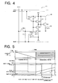
FIG. 4 is a diagram showing the circuit construction of
a pixel according to a second embodiment;
FIG. 5 is a waveform diagram showing the operation of
the circuit construction;
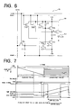
FIG. 6 is a diagram showing the circuit construction of
a pixel according to a third embodiment;
FIG. 7 is a waveform diagram showing the operation of
the circuit construction;
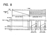
FIG. 8 is a waveform diagram showing the operation of a
fourth embodiment;
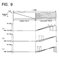
FIG. 9 is a waveform diagram showing the operation of a
fifth embodiment;
FIG. 10 is a block diagram showing the construction of
an organic EL display device according to a sixth embodiment;
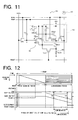
FIG. 11 is a diagram showing the circuit construction of
a pixel according to the sixth embodiment;
FIG. 12 is a waveform diagram showing the operation of
the circuit construction;
FIG. 13 is a diagram showing the circuit construction of
a pixel according to a seventh embodiment;
FIG. 14 is a waveform diagram showing the operation of
the circuit construction;
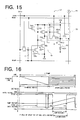
FIG. 15 is a diagram showing the circuit construction of
a pixel according to an eighth embodiment;
FIG. 16 is a waveform diagram showing the operation of
the circuit construction;
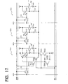
FIG. 17 is a diagram showing the circuit construction of
a plurality of pixels according to a ninth embodiment;
FIG. 18 is a waveform diagram showing the operation of
the circuit construction;
FIG. 19 is a diagram showing the circuit construction of
a pixel according to a tenth embodiment;
FIG. 20 is a waveform diagram showing the operation of
the circuit construction;
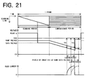
FIG. 21 is a waveform diagram showing the same in the
case where data voltage alters;
FIG. 22 is a diagram showing the circuit construction of
a pixel according to an 11th embodiment;
FIG. 23 is a waveform diagram showing the operation of
the circuit construction;
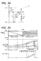
FIG. 24 is a diagram showing the circuit construction of
a pixel according to a 12th embodiment;
FIG. 25 is a waveform diagram showing the operation of
the circuit construction;
FIG. 26 is a waveform diagram showing the same in the
case of an altered data voltage;
FIG. 27 is a waveform diagram for illustrating a
correction operation when the characteristics of the organic
EL element of the circuit construction altered or shifted;
FIG. 28 is a diagram showing the circuit construction of
a pixel according to a 13th embodiment;
FIG. 29 is a waveform diagram showing the operation of
the circuit construction;
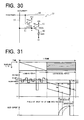
FIG. 30 is a diagram showing the circuit construction of
a pixel according to a 14th embodiment;
FIG. 31 is a waveform diagram showing the operation of
the circuit construction;
FIG. 32 is a diagram showing the circuit construction of
a pixel according to a 15th embodiment;
FIG. 33 is a diagram showing the circuit construction of
a pixel according to a 16th embodiment;
FIG. 34 is a waveform diagram showing the operation of
the circuit construction;
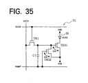
FIG. 35 is a diagram showing the circuit construction of
a pixel according to a 17th embodiment;
FIG. 36 is a diagram showing the circuit construction of
a pixel according to an 18th embodiment;
FIG. 37 is a waveform diagram showing the operation of
the circuit construction;
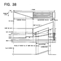
FIG. 38 is a waveform diagram showing the same in the
event of the organic EL characteristics varying or shifting;
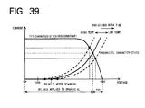
FIG. 39 is a graph showing transistor characteristics
and organic EL'characteristics;
FIG. 40 is a diagram showing the circuit construction of
a pixel according to a 19th embodiment;
FIG. 41 is a diagram showing the circuit construction of
a pixel according to a 20th embodiment;
FIG. 42 is a diagram showing the circuit construction of
a pixel according to a 21st embodiment;
FIG. 43 is a diagram showing the circuit construction of
a pixel according to a 22nd embodiment;
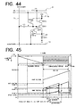
FIG. 44 is a diagram showing the circuit construction of
a pixel according to a 23rd embodiment;
FIG. 45 is a waveform diagram showing the operation of
the circuit construction;
FIG. 46 is a diagram showing the circuit construction of
a pixel according to a 24th embodiment;
FIG. 47 is a waveform diagram showing the operation of
the circuit construction;
FIG. 48 is a diagram showing the circuit construction of
a pixel according to a 25th embodiment;
FIG. 49 is a waveform diagram showing the operation of
the circuit construction;
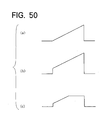
FIG. 50 is a diagram showing various waveforms of ramp
voltages;
FIG. 51 is a diagram showing the circuit construction of
a pixel in a conventional organic EL display device;
FIG. 52 is a diagram showing the circuit construction of
a pixel in an organic EL display device proposed by the
present applicant; and
FIG. 53 is a waveform diagram showing the operation of
the circuit construction.
DETAILED DESCRIPTION OF EMBODIMENTS
Organic EL display devices embodying the present
invention will be described below in detail with reference to
the drawings.
Overall Construction
With reference to FIG. 1, an organic EL display 2
embodying the invention comprises a display panel 5 having a
plurality of pixels arranged in the form of a matrix, and a
scanning driver 3 and a data driver 4 which are connected to
the display panel 5. A TV receiver or like video image source
supplies a video signal to a video signal processing circuit 6,
in which the signal is processed as required for displaying
images, and the resulting video signals of RGB three primary
colors are fed to the data driver 4 of the display 2. The
video signal processing circuit 6 also feeds a horizontal
synchronizing signal Hsync and vertical synchronizing signal
Vsync to a timing signal generating circuit 7. The resulting
timing signal is fed to the scanning driver 3 and the data
driver 4.
The timing signal obtained from the circuit 7 is fed
also to a ramp voltage generating circuit 8, which produces
ramp voltage for driving the EL display 2. The ramp voltage
is supplied to the pixels of the display panel 5. A power
source circuit (not shown) is connected to the circuits,
drivers and EL display shown in FIG. 1.
First Embodiment
A display panel 5 comprises pixels 51 each having the
circuit construction shown in FIG. 2 and arranged in the form
of a matrix. Each of the pixels 51 comprises an organic EL
element 50, a drive transistor TR2 for energizing or
deenergizing the EL element 50 in responses to the input of an
on/off control signal to the gate thereof, a write transistor
TR1 to be brought into conduction when scanning voltage is
applied from the scanning driver to the gate thereof, a
capacitance element C1 to be impressed with data voltage from
the data driver by the conduction of the write transistor TR1,
and a pulse-width modulation control circuit 90 for pulse-width-modulating
the output voltage of the capacitance element
C1 with ramp voltage RAMP to be supplied by the ramp voltage
generating circuit. The capacitance element C1 is connected
at its opposite ends respectively to the drain of the write
transistor TR1 and a ramp voltage supply line. The pulse-width
modulation control circuit 90 comprises an on-control
transistor TR3 for bringing the drive transistor TR2 into
conduction and an off-control transistor TR4 for bringing the
drive transistor TR2 out of conduction.
The organic EL display 2 has a power source VDD of high
potential and a power source VSS of low potential which are
provided in common for the pixels 51. Connected to the power
source VDD of high potential is the source of the drive
transistor TR2 of each pixel 51. The on-control transistor
TR3 and off-control transistor TR4 are connected in parallel
with each other between the power sources VDD and VSS, and a
pair of transistors TR5 and TR6 are connected in series with
each other between the power sources. The junction B of the
two transistors is connected to the gate of the drive
transistor TR2.
The ramp voltage RAMP is supplied to the gate of the on-control
transistor TR3. The output voltage (data voltage) of
the capacitance element C1 is supplied to the gate of the off-control
transistor TR4. Connected to the power source VDD and
the gate of the transistor TR5 are respective opposite ends of
a capacitance element C2, and the source and drain of a reset
transistor TR7. A reset signal line RESET is connected to the
gate of the transistor TR7.
To describe the organic EL display device comprising the
pixels 51 with reference to FIG. 3, the write transistor TR1
is caused to conduct by the supply of scanning voltage SCAN
during the scanning period for the capacitance element C1 to
store data voltage DATA (voltage at point A) therein. The
reset signal RESET thereafter changes from high to low,
bringing the reset transistor TR7 into conduction to set
opposite ends of the capacitance element C2 for the high power
source voltage VDD. As a result, the transistor TR5 is brought
out of conduction. At this time, the other transistors TR2,
TR3, TR4 and TR6 are all nonconducting.
Subsequently during the luminescence period, the ramp
voltage RAMP rises to result in an increased difference
between this voltage and the low-potential power source
voltage VSS. Upon this difference exceeding a threshold level
Vth between the gate of the on-control transistor TR3 and the
source thereof, the transistor TR3 conducts. This brings the
transistor TR6 into conduction, lowering the gate voltage
(voltage a point B) of the drive transistor TR2 and thereby
bringing the transistor TR2 into conduction. Consequently,
current flows from the power source VDD of high potential to
the EL element 50, which starts to luminesce.
Subsequently, with a further rise in the ramp voltage,
the voltage at point A rises, resulting in an increased
difference of this voltage from the low-potential power source
voltage VSS. Upon this difference exceeding the gate-source
threshold level Vth of the off-control transistor TR4, the
transistor TR4 conducts to lower the gate voltage of the
transistor TR6. This brings the transistor TR6 out of
conduction. Simultaneously with this, the transistor TR5
conducts, increasing the gate voltage (voltage at point B) of
the drive transistor TR2 and consequently bringing the
transistor TR2 out of conduction to deenergize the EL element
50 and stop the luminescence.
Thus, the time to stop the luminescence of the organic
EL device 50 alters in accordance with the value of the data
voltage to vary the duration of luminescence in proportion to
the value of the data voltage, whereby expression of multi-level
gradation is realized.
With the pulse-width modulation circuit 90 described,
the on-control transistor TR3 and the off-control transistor
TR4 are positioned in proximity to each other within the same
pixel 51, and the two transistors are produced at the same
time by the same process, such that even if these transistors
involve variations in the gate-source threshold level, the two
transistors exhibit similar variations. Even if the time for
the on-control transistor TR3 to bring the drive transistor
TR2 into conduction differs due to the variation, the time for
the off-control transistor TR4 to bring the drive transistor
TR2 out of conduction thereafter also differs to the same
extent in the same direction.
Accordingly, the period of time from the conduction of
the drive transistor TR2 by the on-control transistor TR3
until the transistor TR2 is brought out of conduction by the
off-control transistor TR4 is accurately in proportion to the
data voltage despite the variations in the threshold level of
the two transistors TR3, TR4.
The signal line extending from the power source VDD of
high potential to the power source VSS of low potential has the
pair of transistors TR5, TR6, and during the scanning period,
the transistor TR5 is brought out of conduction in response to
the input of a reset signal, with the transistor TR6 off.
Subsequently when the transistor TR6 changes from on-state to
off-state in the luminescence period, the transistor TR5 is
brought into conduction at the same time to stop luminescence.
Thus, during the scanning period through the luminescence
period, at least one of the pair of transistors TR5, TR6 is
off to block the current path from the high-potential power
source VDD to the low-potential power source VSS. This obviates
the flow of useless current from the power source VDD to the
power source VSS to thereby reduce power consumption.
Second Embodiment
With reference to FIG. 4, the circuit construction of
each pixel 51 includes a pulse-width modulation circuit 90,
which comprises an on-control transistor TR3 for bringing a
drive transistor TR2 into conduction and an off-control
transistor TR4 for bringing the drive transistor TR2 out of
conduction. The circuit construction is the same as that of
the first embodiment with the exception of the following. The
output voltage (data voltage) of a capacitance element C1 is
supplied to the gate of the on-control transistor TR3, and
ramp voltage RAMP is supplied to the gate of the off-control
transistor TR4. A capacitance element C3 is connected in
parallel with a transistor TR5.
With reference to FIG. 5, in the luminescence period of
the organic EL display device comprising the pixel 51, the
voltage at point A rises with a rise in the ramp voltage RAMP
to produce an increased difference between this voltage and
the low-potential power source voltage Vss. Upon the
difference exceeding the gate-source threshold level Vth of
the on-control transistor TR3, the transistor TR3 conducts.
This brings the transistor TR6 into conduction, lowering the
gate voltage (voltage a point B) of the drive transistor TR2
and thereby bringing the transistor TR2 into conduction.
Consequently, current flows from the power source VDD of high
potential to the EL element 50, which starts to luminesce.
Subsequently, the ramp voltage further rises, producing
an increased difference between this voltage and the low-potential
power source voltage VSS. The difference exceeds the
gate-source threshold level Vth of the off-control transistor
TR4, whereupon the transistor TR4 conducts to lower the gate
voltage of the transistor TR6. This brings the transistor TR6
out of conduction. Simultaneously with this, the transistor
TR5 conducts, increasing the gate voltage (voltage at point B)
of the drive transistor TR2 and consequently bringing the
transistor TR2 out of conduction to deenergize the EL element
50 and stop the luminescence.
Thus, the time to stop the luminescence of the organic
EL device 50 alters in accordance with the value of the data
voltage to vary the duration of luminescence in proportion to
the value of the data voltage, whereby expression of multi-level
gradation is realized.
With the pulse-width modulation circuit 90 described
above, it is likely that the on-control transistor TR3 and the
off-control transistor TR4 will involve variations in the
gate-source threshold level as is the case with the first
embodiment. However, the time for the on-control transistor
TR3 to bring the drive transistor TR2 into conduction and the
time for the off-control transistor TR4 to bring the drive
transistor TR2 out of conduction thereafter will alter to the
same extent in the same direction. Accordingly, the duration
of conduction of the drive transistor TR2 is accurately in
proportion to the data voltage despite the variations in the
threshold level of the two transistors TR3, TR4.
The signal line extending from the power source VDD of
high potential to the power source VSS of low potential has the
pair of transistors TR5, TR6. During the scanning period
through the luminescence period, at least one of the pair of
transistors TR5, TR6 is off to block the current path from the
high-potential power source VDD to the low-potential power
source VSS. This obviates the flow of useless current from the
power source VDD to the power source VSS to thereby reduce
power consumption.
Third Embodiment
With reference to FIG. 6, the circuit construction of
each pixel 51 includes a pulse-width modulation circuit 90,
which comprises an on-control transistor TR3 for bringing a
drive transistor TR2 into conduction and an off-control
transistor TR4 for bringing the drive transistor TR2 out of
conduction. The organic EL display 2 has a power source VDD of
high potential and a power source VSS of low potential which
are provided in common for the pixels 51. Connected to the
power source VDD of high potential is the source of the drive
transistor TR2 of each pixel 51. The on-control transistor
TR3 and off-control transistor TR4 are connected in parallel
with each other between the power sources VDD and VSS, and a
transistor TR5 and a capacitance element C4 are connected in
series with each other between the power sources. The
junction B of the transistor TR5 and the capacitance element
C4 is connected to the gate of the drive transistor TR2.
Ramp voltage RAMP is supplied to the gate of the on-control
transistor TR3. The output voltage (data voltage) of
a capacitance element C1 is supplied to the gate of the off-control
transistor TR4. Connected to the power source VDD of
high potential and the gate of the transistor TR5 are
respective opposite ends of a capacitance element C2, and the
source and drain of a reset transistor TR7. A reset signal
line RESET is connected to the gate of the transistor TR7.
A reset transistor TR8 has its source and drain
connected respectively to the high-potential power source VDD
and one end (point B) of the capacitance element C4. The
reset signal line RESET is connected to the gate of the
transistor TR8. A reset transistor TR9 has its source and
drain connected respectively to the high-potential power
source VDD and the other end of the capacitance element C4. The
reset signal line RESET is connected to the gate of the
transistor TR9.
With reference to FIG. 7, during the scanning period of
the organic EL display device comprising the pixels 51, a
write transistor TR1 is caused to conduct by the supply of
scanning voltage SCAN for the capacitance element C1 to store
data voltage DATA (voltage at point A) therein. The reset
signal RESET thereafter changes from high to low, bringing the
three reset transistors TR7, TR8 and TR9 into conduction to
set opposite ends of the capacitance element C2 for the high
potential VDD, and opposite ends of the capacitance element C4
for the high-potential power source voltage VDD. As a result,
the transistor TR5 is brought out of conduction. At this time,
the other transistors TR2, TR3, TR4 are all nonconducting.
Subsequently during the luminescence period, the ramp
voltage RAMP rises to result in an increased difference
between this voltage and the low-potential power source
voltage VSS. Upon the difference exceeding the gate-source
threshold level Vth of the on-control transistor TR3, the
transistor TR3 conducts. This lowers the potential across
opposite ends of the capacitance element C4, and a drop in the
gate voltage (voltage at point B) brings the drive transistor
TR2 into conduction. Consequently, current flows from the
power source VDD of high potential to the EL element 50, which
starts to luminesce. Incidentally, the transistor TR5 has its
gate voltage held at a high potential by the capacitance
element C2 and remains nonconducting.
Subsequently, with a further rise in the ramp voltage,
the voltage at point A rises, producing an increased
difference between this voltage and the low-potential power
source voltage VSS . The difference exceeds the gate-source
threshold level Vth of the off-control transistor TR4,
whereupon the transistor TR4 conducts to lower the gate
voltage of the transistor TR5. This brings the transistor TR5
into conduction. As a result, the gate voltage (voltage at
point B) of the drive transistor TR2 rises to bring the
transistor TR2 out of conduction, deenergize the EL element 50
and stop the luminescence.
Thus, the time to stop the luminescence of the organic
EL device 50 alters in accordance with the value of the data
voltage to vary the duration of luminescence in proportion to
the value of the data voltage, whereby expression of multi-level
gradation is realized.
With the pulse-width modulation circuit 90 described,
even if the on-control transistor TR3 and the off-control
transistor TR4 involve variations in the gate-source threshold
level as is the case with the first and second embodiments,
the duration of conduction of the drive transistor TR2
accurately corresponds to the data voltage. The signal line
extending from the power source VDD of high potential to the
power source VSS of low potential has the capacitance element
C4, so that during the scanning period through the
luminescence period, no useless current flows from the power
source VDD and to the power source VSS to thereby reduce power
consumption.
Fourth Embodiment
The circuit construction of each pixel 51 according to
this embodiment is the same as that of the first, second or
third embodiment, whereas ramp voltage is produced twice, i.e.,
in the first half and second half of the luminescence period
as shown in FIG. 8. In this way, luminescence can be effected
separately in the first half and the in the second half. This
serves to suppress a color flicker (the phenomenon that an
object moving at a high speed exhibits a color change at its
edge) due to differences in the luminescence time of images of
R, G, B.
Fifth Embodiment
The circuit construction of each pixel 51 according to
this embodiment is the same as that of the first, second or
third embodiment, whereas ramp voltages which are different in
slope are supplied for pixels of three primary colors (R, G,
B) as shown in FIG. 9, (a) to (c).
Thus, ramp voltages of different slopes are used for the
respective pixels of R, G, B, whereby the white balance is
adjustable without altering the data voltage. Furthermore,
the three patterns of FIG. 9, (a), (b), (c) are changed over
for every frame, whereby a color flicker (the phenomenon that
an object moving at a high speed exhibits a color change at
its edge) due to differences in the luminescence time of
images of R, G, B can be suppressed.
Sixth Embodiment
FIG. 10 shows this embodiment, i.e., an organic EL
display device comprising a display panel 5, a constant-current
driver 91 connected to the display panel 5 for causing
a constant current to flow through the organic EL elements 50
of respective pixels by a current program circuit to be
described later, and a pulse-width modulation control circuit
for controlling the energization of the organic EL element 50.
In the EL display device, the pulse-width modulation
control circuit 90 constituting each of pixels 51 has the
constant-current driver 91 connected thereto via a current
program circuit 92 as shown in FIG. 11. The control circuit
90 comprises an on-control transistor TR11 for causing a
current-on transistor TR13 to conduct, and an off-control
transistor TR12 for bringing out of conduction a transistor
TR14 constituting the current program circuit 92. The
current-on transistor TR13 is connected to a power source VDD
via the transistor TR14 constituting the current program
circuit 92.
Connected to the power source VDD and the gate of the
transistor TR14 are respective opposite ends of a capacitance
element C11 and the source and drain of the off-control
transistor TR12. Further connected to the power source VDD and
the gate of the current-on transistor TR13 are respective
opposite ends of a capacitance element C12 and the source and
drain of the on-control transistor TR11.
A junction of the capacitance element C11 and the drain
of the off-control transistor TR12 is connected to the
constant-current driver 91 via transistors TR15 and TR16. A
junction of the transistors TR15 and TR16 is connected to the
drain of the current-on transistor TR13. A junction of the
gate of the current-on transistor TR13 and the drain of the
on-control transistor TR11 is connected to a junction of the
current-on transistor TR13 and the organic EL element 50 via a
transistor TR17, to the gate of which is connected a resent
signal line RESET.
With EL display device comprising the pixel 51, a reset
signal RESET supplied brings the transistor TR17 into
conduction first during a reset period as shown in FIG. 12 to
bring the current-on transistor TR13 out of conduction. At
this time, transistors TR1, TR11, TR12, TR14, TR15 and TR16
are nonconducting.
During the subsequent scanning period, the supply of
scanning voltage SCAN brings the write transistor TR1 into
conduction to store data voltage DATA (voltage at point A) in
a capacitance element C1. The transistors TR15 and TR16 are
also brought into conduction, and the transistor TR14 of the
current program circuit 12 is gradually initiated into
conduction. As a result, a programmed current starts to flow
from the power source VDD toward the current driver 91 via the
transistors TR14 and TR16, eventually ensuring a gate voltage
for the transistor TR14. A charge corresponding to the
programmed current is stored in the capacitance element C11.
The gate voltage of the on-control transistor TR11 drops
with a drop in ramp voltage RAMP during the subsequent
luminescence period, producing an increased difference from
the power source voltage VDD. Upon the difference exceeding
the gate-source threshold level of the on-control transistor
TR11, this transistor TR11 conducts, consequently bringing the
current-on transistor TR13 into conduction and causing
programmed current to flow from the power source VDD to the EL
element 50 via the transistors TR14 and TR13 to start
luminescence.
The ramp voltage further drops to produce an increased
difference from the power source voltage VDD. Upon the
difference exceeding the gate-source threshold level of the
off-control transistor TR12, the transistor TR12 conducts, and
the transistor TR14 of the current program circuit 92 is
brought out of conduction. Consequently, the EL element 50 is
deenergized to stop luminescence.
Thus, the time to start the luminescence of the organic
EL device 50 alters in accordance with the value of the data
voltage to vary the duration of luminescence in proportion to
the value of the data voltage, whereby expression of multi-level
gradation is realized.
With the pulse-width modulation circuit 90 described,
the duration of energization of the organic EL element 50
accurately corresponds to the data voltage despite the
variations to be involved in the gate-source threshold levels
of the on-control transistor TR11 and the off-control
transistor TR12. The current from the power source VDD flows
through the EL element 50 only during a period of time also
corresponding to the data voltage. This obviates the flow of
useless current to thereby reduce power consumption.
Seventh Embodiment
With reference to FIG. 13, the circuit construction of
each of pixels 51 includes a pulse-width modulation circuit 90,
which comprises an on-control transistor TR11 and an off-control
transistor TR12. The circuit construction is the same
as that of the sixth embodiment except that ramp voltage RAMP
is supplied to the gate of the on-control transistor TR11, and
that the output voltage (data voltage) of a capacitance
element C1 is supplied to the gate of the off-control
transistor TR12.
With reference to FIG. 14 showing the operation of the
EL display device comprising the pixel 51, the gate voltage of
the on-control transistor TR11 drops with a drop in the ramp
voltage RAMP during the luminescence period, producing an
increased difference from the power source voltage VDD. Upon
the difference exceeding the gate-source threshold level of
the on-control transistor TR11, this transistor TR11 conducts,
consequently bringing the current-on transistor TR13 into
conduction and causing current to flow from the power source
VDD to the EL element 50 via the transistors TR14 and TR13 to
start luminescence.
The ramp voltage further drops to produce an increased
difference from the power source voltage VDD. Upon the
difference exceeding the gate-source threshold level of the
off-control transistor TR12, the transistor TR12 conducts, and
the transistor TR14 of the current program circuit 92 is
brought out of conduction. Consequently, the EL element 50 is
deenergized to stop luminescence.
Thus, the time to stop the luminescence of the organic
EL device 50 alters in accordance with the value of the data
voltage to vary the duration of luminescence in proportion to
the value of the data voltage, whereby expression of multi-level
gradation is realized. With the pulse-width modulation
circuit 90 described, the duration of energization of the
organic EL element 50 accurately corresponds to the data
voltage. The current from the power source VDD flows through
the EL element 50 only during a period of time also
corresponding to the data voltage. This obviates the flow of
useless current to thereby reduce power consumption.
Eighth Embodiment
With reference to FIG. 15, the circuit construction of
each pixel 51 of this embodiment comprises the pulse-width
modulation circuit 90 of the first embodiment shown in FIG. 2,
and the current program circuit 92 shown in FIG. 11 and
connected to the circuit 90. This embodiment operates in the
same manner as the first embodiment as shown in FIG. 16 to
control the energization of the organic EL element 50.
Ninth Embodiment
With reference to FIG. 17, this embodiment, i.e., an
organic EL display device, comprises pixels 51 which are
divided into groups of pixels 51a, 51b, 51c which are adjacent
to one another. One of the adjacent pixels, i.e., the pixel
51a, has a circuit construction incorporating a pulse-width
modulation circuit 90, while the other pixels 51b, 51c have a
circuit construction incorporating only part of the circuit 90.
The pixels 51a, 51b, 51c of the same pixel group are in common
with respect to the other circuit portion.
The pulse-width modulation control circuit 90
incorporated in the pixel 51a comprises an on-control
transistor TR11 for bringing a drive transistor TR2 into
conduction and an off-control transistor TR12 for bringing the
drive transistor TR2 out of conduction. The pixel 51a has
connected thereto a power source VDD of high potential and a
power source VSS of low potential. An organic EL element 50 is
connected to the power source VDD of high potential via the
drive transistor TR2.
The on-control transistor TR11 and off-control
transistor TR12 are connected in parallel with each other
between the power sources VDD and VSS, and a capacitance
element C21 and two transistors TR21 and TR22 in series
therewith are connected between the power sources. A junction
B of the off-control transistor TR12 and the capacitance
element C21 is connected to the gate of the drive transistor
TR2. The high-potential power source VDD is connected to the
drain of a transistor TR21 via a transistor TR23. A first
reset signal line RST1 is connected to the gates of the two
transistors TR23, TR21.
A transistor TR24 has a drain and a source which are
connected respectively to the gate of the transistor TR22 and
the low-potential power source VSS. A second reset signal line
RST2 is connected to the gate of the transistor TR24. Ramp
voltage RAMP is supplied to the gate of the on-control
transistor TR11. The output voltage (data voltage) of a
capacitance element C1 is supplied to the gate of the off-control
transistor TR12.
On the other hand, only the off-control transistor TR12
and the capacitance element C21, which are components of the
pulse-width modulation control circuit 90, are provided in
each of the pixels 51b, 51c adjacent to the pixel 51a. The
capacitance elements C21 of the respective pixels are
connected to one another at their low-potential side.
With the organic EL display device comprising the pixels
51a, 51b, 51c, the write transistor TR1 of each pixel is
brought into conduction by the supply of scanning voltage SCAN
during the scanning period, and a charge corresponding to data
voltage (voltage at point A) is stored in the capacitance
element C1 to write data thereto as shown in FIG. 18.
Incidentally at this time, the transistors TR2, TR11, TR12,
TR21, TR22, TR23 and TR24 are all nonconducting.
Subsequently during the luminescence period, the ramp
voltage RAMP drops to result in an increased difference
between this voltage and the high potential VDD. Upon the
difference exceeding the gate-source threshold level Vth of
the on-control transistor TR11, the transistor TR11 conducts.
This brings the transistor TR22 into conduction and the
transistor TR21 also into conduction at the same time to lower
the voltage across opposite ends of the capacitance elements
C21 in the pixels. Consequently, the drive transistor TR2 of
each pixel is brought into conduction, causing current to flow
from the power source VDD of high potential to the EL element
50, which starts to luminesce.
Subsequently, with a further drop in the ramp voltage,
the voltage at point A drops, producing an increased
difference between this voltage and the high potential VDD.
The difference exceeds the gate-source threshold level Vth of
each off-control transistor TR12, whereupon the transistor
TR12 conducts to raise the voltage at point B. As a result,
the drive transistor TR2 is brought out of conduction to
deenergize the EL element 50 and stop the luminescence.
In the subsequent reset period, the first reset signal
RST1 changes from high to low, whereby the transistor TR23 is
brought into conduction. At the same time, the transistor
TR21 is brought out of conduction, and the potential at the
junction of the transistor TR21 and the capacitance elements
C21 of the pixels rises to set the opposite ends of the
capacitance elements C21 for the high potential.
When the ramp voltage then rises to the high level, the
on-control transistor TR11 and the off-control transistor TR12
are brought out of conduction. Subsequently, the second reset
signal RST2 becomes high only for a specified period of time,
whereby the transistor TR24 is brought into conduction and the
transistor TR22 is brought out of conduction. The first reset
signal RST1 thereafter changes to high, thereby bringing the
transistor TR23 out of conduction. This mode of control
prevents current from straightforwardly flowing between the
two power sources VDD and VSS .
With the organic EL display device described above, the
pixel 51a among pixels 51a, 51b, 51c which are adjacent to one
another has the pulse-width modulation control circuit 90 in
its entirety, whereas the other pixels 51b, 51c each have only
some components of the circuit 90. This construction serves
to reduce the number of transistors in the entire display
panel, consequently improving the opening ratio of the display
panel and yield.
Tenth Embodiment
The drive transistor included in the first to ninth
embodiments is omitted from this embodiment, and an on-control
transistor (the first transistor to be described below) serves
both to drive an organic EL element 50 and to control the
energization of the organic EL element 50.
With reference to FIG. 19, each of pixels 51 has an
organic EL element 50, a write transistor TR1 of the p-channel
type having a gate to be impressed with scanning voltage SCAN,
a capacitor C1 to be impressed with data voltage DATA by the
conduction of the write transistor TR1 for holding the voltage,
a first transistor TR31 of the p-channel type provided in
series with a power supply line 55 extending from a power
supply VDD to the EL element 50 and to be brought into
conduction upon the difference between the gate voltage
thereof and the power source voltage VDD exceeding a
predetermined threshold value Vth, and a second transistor
TR32 of the p-channel type to be brought into conduction upon
the difference between the gate voltage thereof and the power
source voltage VDD exceeding a predetermined threshold value
Vth to bring the first transistor TR31 out of conduction.
Applied to the gate of the first transistor TR31 is a voltage
(voltage at point A) corresponding to the sum of ramp voltage
RAMP and the output voltage of the capacitor. The ramp
voltage RAMP is applied to the gate of the second transistor
TR32.
With reference to FIG. 20, the write transistor TR1 is
brought into conduction by the application of the scanning
voltage SCAN in the first-half scanning period of 1 frame,
whereupon the potential at point A is set for the data voltage
to charge the capacitor C1. Subsequently when the ramp
voltage RAMP gradually drops in the second-half luminescence
period of 1 frame, the voltage at point A also gradually drops
along with the ramp voltage at the same rate of reduction.
Upon the difference between the power source voltage VDD and
the data voltage consequently exceeding the threshold value
Vth of the first transistor TR31, this transistor TR31
conducts, starting to energize the EL element 50 from the
power source VDD. As a result, the current flowing through the
EL element 50 gradually increases as seen in FIG. 20, causing
the element %50 to luminesce.
Upon the difference between the power source voltage VDD
and the ramp voltage RAMP thereafter exceeding the threshold
value Vth of the second transistor TR32, the second transistor
TR32 conducts, with the result that the potential at point A
increases toward the power source voltage VDD to bring the
first transistor TR31 out of conduction. As a result, the
supply of current to the EL element 50 from the power source
VDD is discontinued to stop the luminescence of the element 50.
When 1 frame completion time is reached, the ramp voltage
resumes the original value, permitting the voltage at point A
to also resume the original value, followed by the operation
for the next frame.
FIG. 21 shows variations in voltages and variations in
the current flowing through the organic EL element 50 in the
event of the data voltage altering. The luminescence period
of the EL element 50 thus varies with the variation of the
data voltage, whereby multi-level gradation of images is
expressed. For example when the threshold value of the first
transistor TR31 involves a positive variation, the time to
start the luminescence of the EL element 50 is delayed as
indicated in broken lines in FIGS. 20 and 21, but since the
time to stop the luminescence is also delayed by the same
length of time, the luminescence period of the EL element 50
is of the same length corresponding to the data voltage
despite the variation in the threshold values of the two
transistors TR31, TR32. This obviates display irregularities
to show images of high quality.
Further the first transistor TR31 can be made to operate
in either one of the linear region and the saturation region
by altering the cathode potential CV of the EL element 50. By
allowing the first transistor TR31 to operate in the linear
region, it is possible to ensure reduced power consumption,
while the first transistor TR31 can be made less susceptible
to the influence of temperature or alterations with time when
allowed to operate in the saturation region.
Further because the first transistor TR31 is provided on
the power supply line 55 in series therewith for energizing or
deenergizing the organic EL element 50, the current from the
power source VDD flows only through the supply line 55. This
serves to obviates waste of current. Incidentally, the write
transistor TR1 need not always be of the p-channel type, but
can be of the n-channel type, or can be a CMOS switch
comprising a n-channel circuit and a p-channel circuit as
connected in parallel with each other.
11th Embodiment
With reference to FIG. 22, each pixel 51 has an organic
EL element 50, a write p-channel transistor TR1, a capacitor
C1 to be caused to hold data voltage DATA therein by the
conduction of the write transistor TR1, a first p-channel
transistor TR31 provided in series with a power supply line 55
and to be brought into conduction upon the difference between
the gate voltage thereof and power source voltage VDD exceeding
a predetermined threshold value Vth, and a second p-channel
transistor TR32 to be brought into conduction upon the
difference between the gate voltage thereof and the power
source voltage VDD exceeding a predetermined threshold value
Vth to bring the first transistor TR31 out of conduction. The
present embodiment is the same as the tenth embodiment in this
construction. However, two kinds of ramp voltages RAMP1 and
RAMP2 which are different in rate of variation are supplied to
each pixel 51. A capacitor C1 is interposed between a line
for supplying the first ramp voltage RAMP1 and point A, and
the second ramp voltage RAMP2 is applied to the gate of the
second transistor TR32.
With reference to FIG. 23, the voltage at point A drops
with a drop in the first ramp voltage RAMP1 in the
luminescence period. In the case where the capacitor C1 has a
small capacitor, the rate of drop of the voltage at point A is
smaller than that of the ramp voltage RAMP1. Accordingly, the
second ramp voltage RAMP2 is prepared which is the same as the
voltage at point A in variation rate, and is applied to the
gate of the second transistor TR32 to thereby obtain a
luminescence period in accordance with the data voltage.
12th Embodiment
FIG. 24 shows a pixel 51 having a write transistor TR1,
first transistor TR31 and second transistor TR32, each of
which is an n-channel transistor. The first transistor TR31
and the second transistor TR32 are connected to point B so as
to be brought into conduction upon the difference between the
gate voltage and the high-potential-side terminal voltage
(voltage at point B) of an organic EL element 50 exceeding a
predetermined threshold value. A voltage (voltage at point A)
corresponding to the sum of ramp voltage RAMP and the output
of a capacitor C1 is applied to the gate of the first
transistor TR31. The ramp voltage RAMP is applied to the gate
of the second transistor TR32.
With reference to FIG. 25, the write transistor TR1 is
brought into conduction by the application of scanning voltage
SCAN during the scanning period, whereupon the potential at
point A is set for data voltage, whereby the capacitor C1 is
charged. During the subsequent luminescence period, the ramp
voltage RAMP gradually rises, and the voltage at point A also
gradually rises with the ramp voltage at the same rate.
Consequently, upon the difference between the voltage at point
B and the data voltage exceeding the threshold value Vth of
the first transistor TR31, the first transistor TR31 conducts,
permitting a power supply VDD to start to energize the EL
element 50. As a result, the current flowing through the EL
element 50 gradually increases as shown in FIG. 25, causing
the EL element 50 to luminesce. Incidentally in the circuit
construction shown in FIG. 25, the potential at point B rises
with an increase in the current flowing through the EL element
50.
When the difference between the voltage at point B and
the ramp voltage RAMP thereafter exceeds the threshold value
Vth of the second transistor TR32, the second transistor TR32
conducts, thereby causing the potential at point A to drop
toward the potential at point B to bring the first transistor
TR31 out of conduction. As a result, the power source VDD
stops energizing the organic EL element 50 to stop the
luminescence of the element 50. Upon completion of 1 frame
period, the ramp voltage returns to the original level, and
the voltage at point A also resumes the original level along
with the ramp voltage. An operation for the next frame then
follows.
FIG. 26 shows variations in voltages and in the current
flowing through the organic EL element in the event of the
data voltage altering. The luminescence period of the EL
element 50 varies with the variation of the data voltage,
whereby images are displayed with multi-level gradation thus
realized. For example, if the threshold value of the first
transistor TR31 involves a variation in the positive direction,
the time to start the luminescence of the EL element 50 is
delayed as indicated in broken lines in FIGS. 25 and 26, but
the time to stop the luminescence of the element 50 is also
delayed by the same amount, with the result that the EL
element 50 is luminescent for a period in proportion to the
data voltage despite the variations in the threshold values of
the two transistors TR31, TR32. Display irregularities are
thus avoidable to provide images with a high quality.
With the circuit construction of the pixel 51 shown in
FIG. 24, even if the characteristics of the organic EL element
50 vary due to variations in temperature or variations with
time to result in, for example, a lower potential at point B
during the scanning period as indicated by an arrow in FIG. 27,
the waveform of the current flowing through the EL element 50
merely undergoes translation since the drain of the second
transistor TR32 is connected to point B. Display
irregularities are unlikely to occur, therefore.
13th Embodiment
With the pixel 51 shown in FIG. 28, the drain of the
second transistor TR32 connected to point B in the above
embodiment is connected to the power source VSS of low
potential. Upon the difference between the power source
voltage VSS and ramp voltage RAMP exceeding the threshold value
Vth of the second transistor TR32 in this circuit construction
as shown in FIG. 29, the second transistor TR32 conducts,
bringing the first transistor TR31 out of conduction.
Consequently, the power source VDD stops energizing the organic
EL element 50 for the element 50 to discontinue luminescence.
As indicated in broken lines in FIG. 29, the
luminescence period of the EL element 51 remains the same in
length in proportion to the data voltage despite the
variations in the threshold values of the two transistors TR31,
TR32. Despite the variations in the characteristics of the
two transistors TR31, TR32, therefore, the duration of
energization of the EL element 50 is in proportion to the
value of the data voltage and involves no likelihood of
display irregularities. The first transistor TR31 is
positioned on and in series with the power supply line 55 to
energize or deenergize the EL element 50, so that the current
from the power source VDD flows only through the power supply
line 55, hence occurrence of no useless current.
14th Embodiment
The pixel 51 shown in FIG. 30 has a first signal line 56
for applying scanning voltage SCAN in the first half of 1
frame period and ramp voltage RAMP2 in the second half of 1
frame period, and a second signal line 57 for applying data
voltage DATA in the first half of 1 frame period and ramp
voltage RAMP1 in the second half of 1 frame period. A first
transistor TR31 is provided on a power supply line 55 in
series therewith, and the second signal line 57 is connected
via a capacitor C1 to point A connected to the gate of the
first transistor TR31. The drain of a second transistor rTR32
is also connected to point A. Connected to the source of the
second transistor TR32 is a second power source VCC of higher
voltage than a first power source VDD connected to the power
supply line 55. The first signal line 56 is connected to the
gate of the second transistor TR32.
With reference to FIG. 31, the voltage at point A varies
with the data voltage of each scanning line to be applied to
the second signal line 57 during the scanning period. When
the gate of the second transistor TR32 is impressed with the
scanning voltage from the first signal line 56, the transistor
TR32 conducts, setting the voltage at point A for the voltage
VCC of the second power source. At this time, the capacitor C1
is given a potential difference in accordance with the data
voltage relative to the power source voltage VCC. The
potential difference is maintained in spite of the subsequent
variations in the voltage at point A.
In the luminescence period, the voltage at point A is
set first for a voltage in accordance with the difference
between the voltage held in the capacitor C1 and the ramp
voltage RAMP1, and the voltage at point A gradually drops with
a reduction in the ramp voltage RAMP1. Upon the difference
between the power source voltage VDD and the voltage at point A
consequently exceeding the threshold value Vth of the first
transistor TR31, the transistor TR31 conducts, allowing the
power source VDD to energize the organic EL element 50. As a
result, the current flowing through the EL element 50
gradually increases, and the EL element 50 luminesces.
The difference between the second power source voltage
VCC and the ramp voltage RAMP2 thereafter exceeds the threshold
value Vth of the second transistor TR32, whereupon the second
transistor TR32 conducts, thereby bringing the first
transistor TR31 out of conduction. Consequently, the passage
of current from the power source VDD to the EL element 50 is
discontinued to cease the luminescence of the element 50.
With the pixel 51 described, the luminescence period of
the organic EL element 50 remains the same in length in
proportion to the data voltage despite variations in the
threshold values of the two transistors TR31, TR32 as
indicated in broken lines in FIG. 31. Thus, the duration of
energization of the EL element 50 is in proportion to the
value of the data voltage even if the characteristics of the
two transistors TR31, TR32 involve variations, hence no
likelihood of display irregularities. Furthermore, the first
transistor TR31 is positioned on the power supply line 55 in
series therewith for energizing or deenergizing the EL element
50, so that that the current from the power source VDD flows
only through the supply line 55. The flow of useless current
is therefore avoidable.
15th Embodiment
FIG. 32 shows a pixel 51, wherein an n-channel
transistor serves as each of the two p-channel transistors
TR31, TR32 of the above embodiment to realize exactly the same
circuit operation.
16th Embodiment
According to this embodiment, ramp voltage is applied to
a first transistor TR31 for starting energization, while data
voltage is applied to a second transistor TR32 for stopping
energization to control the deenergizing timing.
With reference to FIG. 33, each pixel 51 has an organic
EL element 50, a write transistor TR1 to be impressed with
scanning voltage SCAN for conduction, a first capacitor C2 to
be impressed with data voltage by the conduction of the write
transistor TR, the first transistor TR31 provided on and
positioned in series with a power supply line 55 extending
from a power source VDD to the EL element 50, the second
transistor TR32 for bringing the first transistor TR31 out of
conduction, a third transistor TR33 for applying the voltage
of the power source to the gate of the first transistor 31
when brought into conduction by the application of scanning
voltage, and a second capacitor C3 interposed between the gate
of the first transistor TR31 and a ramp voltage supply line.
The gate of the first transistor TR31 is connected to
the ramp voltage supply line via the second capacitor C3 and
coupled to the power source VDD by way of the second and third
transistors TR32 and TR33. The gate of the second transistor
TR32 is coupled to the ramp voltage supply line via the first
capacitor C2. The gate of the third transistor TR33 is
connected to a scanning voltage supply line.
With reference to FIG. 34, when the write transistor TR1
and the third transistor TR33 of the pixel 51 are brought into
conduction by the application of scanning voltage SCAN during
the scanning period, the first capacitor C2 is charged with
the data voltage to set the output end (point A) thereof for
the data voltage, and point B connected to the gate of the
first transistor TR31 is set for the power source voltage VDD.
The potentials at point A and point B gradually drop as
the ramp voltage RAMP gradually drops during the luminescence
period. Upon the difference between the power source voltage
VDD and the voltage at point B exceeding the threshold value
Vth of the first transistor TR31, the first transistor TR31
conducts, starting to energize the EL element 50. The
difference between the power source voltage VDD and the voltage
at point A thereafter exceeds the threshold value Vth of the
first transistor TR32, whereupon the second transistor TR32
conducts, raising the voltage at point B to the power source
voltage VDD. This brings the first transistor TR31 out of
conduction to deenergize the EL element 50.
The pixel 51 described has the second capacitor C3
between the ramp voltage supply line and point B, hence no
collision between the ramp voltage RAMP and the power source
voltage VDD.
With the pixel 51 described, the luminescence period of
the organic EL element 50 remains the same in length in
proportion to the data voltage despite variations in the
threshold values of the two transistors TR31, TR32 as
indicated in broken lines in FIG. 34. Thus, the duration of
energization of the EL element 50 is in proportion to the
value of the data voltage, hence no likelihood of display
irregularities. Furthermore, the first transistor TR31 is
positioned on the power supply line 55 in series therewith for
energizing or deenergizing the EL element 50, so that that the
current from the power source VDD flows only through the supply
line 55. The flow of useless current is therefore avoidable.
17th Embodiment
FIG. 35 shows an embodiment wherein an organic EL
element 50 is provided at a position of higher potential (VDD)
than a first transistor TR31 for driving, with the sources of
the first transistor TR31 and second transistor TR32 connected
to a power source Vss of low potential. Like the above
embodiment, this embodiment also obviates display
irregularities and the flow of useless current.
18th Embodiment
To be described below are 18th to 24th embodiments
wherein the display element is adapted to luminesce in a
quantity in proportion to the data voltage despite variations
in the characteristics of the EL element.
With reference to the 18th embodiment shown in FIG. 36,
each pixel 51 has a first signal line 61 for applying scanning
voltage SCAN in the first half of 1 frame period and high
selected voltage SEL in the second half of 1 frame period, a
second signal line 62 for applying data voltage DATA in the
first half of 1 frame period and first ramp voltage RAMP1 in
the second half of 1 frame period, a third signal line 63 for
applying a reset signal RST, and a fourth signal line 64 for
applying second ramp voltage RAMP2.
The pixel 51 further has an organic EL element 50, a
write transistor TR1, a capacitor C1 to be impressed with the
data voltage DATA from the second signal line 62 by the
conduction of the write transistor TR1, a first transistor
TR31 provided on a power supply line 6 extending from a power
source VDD of high potential to the EL element 50, a second
transistor TR32 interposed between the output end (point B) of
the capacitor C1 and one end (point C) of the EL element 50,
and a third transistor TR34 provided between the output end
(point B) of the capacitor C1 and a low-potential power source
Vss.
The first signal line 61 is connected to the gate of the
write transistor TR1. The drain of the write transistor TR1
is connected via the capacitor C1 to the gate of the first
transistor TR31. The fourth signal line 64 is connected to
the gate of the second transistor TR32. The third signal line
63 is connected to the gate of the third transistor TR34.
As shown in FIG. 37, one frame is divided into a
scanning period, luminescence period and reset period. The
second ramp voltage RAMP2 drops first in the reset period to
thereby bring the second transistor TR32 out of conduction,
whereupon the reset signal RST changes to high, causing the
third transistor TR34 to conduct to permit the potential at
point B to drop to the power source voltage Vss. The second
ramp voltage RAMP2 thereafter rises, bringing the second
transistor TR3 into conduction. This couples point B to point
C to give these points approximately the same potential. The
first ramp voltage RAMP1 drops while the reset signal RST is
high.
During the scanning period of the next frame, the write
transistor TR1 is brought into conduction by the application
of scanning voltage SCAN, whereupon the potential at the
output end (point A) of the write transistor TR1 rises to the
data voltage. This raises the potential at point B and the
potential at point C to the luminescence starting voltage of
the EL element. At this time, the first transistor TR31 is
nonconducting, and the second transistor TR32 is in conduction,
with the result that the charge in the capacitor C1 flows to
the cathode through the second transistor TR32 and the EL
element 50. Accordingly the rise in the potential at point B
and point C is smaller than the rise of the potential at point
A. The potential at point B is set for the power source
voltage VSS by the reset operation in the reset period and is
unlikely to drop below the voltage VSS. By raising the
potential at point A to the data voltage during the subsequent
scanning period, the potentials at point B and point C can be
raised to the luminescence starting voltage of the EL element
50.
Simultaneously with completion of the scanning period,
the second ramp voltage RAMP2 drops, consequently bringing the
second transistor TR32 out of conduction. During the
subsequent luminescence period, the first ramp voltage RAMP1
and the second ramp voltage RAMP2 start to rise.
The potential at point A consequently rises as changed
over from data voltage to first ramp voltage RAMP1, and the
potential at point B rises along with this potential. As a
result, upon the difference between the potential at point B
and the potential at point C exceeding the threshold level Vth
of the first transistor TR31, the transistor TR31 conducts,
starting to energize the EL element 50 for luminescence.
With a rise in the second ramp voltage RAMP2, the
difference between this voltage and the potential at point C
thereafter exceeds the threshold value Vth of the second
transistor TR32, whereupon the second transistor TR32 conducts.
This brings the first transistor TR31 out of conduction to
deenergize the EL element 50 to complete the luminescence of
the element 50.
With the pixel 51 described, the luminescence period of
the organic EL element 50 remains the same in length in
proportion to the data voltage despite variations in the
threshold values of the two transistors TR31, TR32 as
indicated in broken lines in FIG. 37. Thus, the duration of
energization of the EL element 50 is in proportion to the
value of the data voltage, hence no likelihood of display
irregularities. Furthermore, the first transistor TR31 is
positioned on the power supply line 6 in series therewith for
energizing or deenergizing the EL element 50, so that that the
current from the power source VDD flows only through the supply
line 6. The flow of useless current is therefore avoidable.
Additionally, the problem due to the temperature
variations or variations with time which are involved in the
organic EL element 50 can be overcome by the present
embodiment. Stated more specifically with reference to FIG.
39, the temperature variations or variations with time of the
organic EL element vary the organic EL characteristics,
consequently resulting in an altered point of operation and an
altered quantity of luminescence. This problem is overcome by
feeding back the potential (terminal voltage at the
luminescence starting time) at point C after scanning to the
duration of the EL element 50 according to the invention.
FIG. 38 shows the operation of the EL element when the
organic EL characteristics shift toward the right owing to
temperature variations or variations with time of the organic
EL element. As illustrated, the application of scanning
voltage SCAN during the scanning period raises the potential
at point A to the data voltage, consequently slightly raising
the potential at point B and the potential at point C. The
rises in the potentials at point B and point C are slightly
greater owing to the shift of the organic EL characteristics
than in the absence of shift (FIG. 37) as indicated by an
arrow.
In the subsequent luminescence period, the first ramp
voltage RAMP1 and the second ramp voltage RAMP2 start to rise,
and upon the difference between the potential at point B and
the potential at point C exceeding the threshold value Vth of
the first transistor TR31, this transistor TR31 conducts,
starting to energize the EL element 50 and causing the element
50 to luminesce. This time point is the same as in the case
where there is no characteristics shift (FIG. 37).
Owing to a rise in the second ramp voltage RAMP2, the
difference between the second ramp voltage RAMP2 and the
potential at point C thereafter exceeds the threshold level
Vth of the second transistor TR32, whereupon the transistor
TR32 conducts. However, the potential at point C which is
higher than in the absence of the characteristics shift as
stated above delays the time for the difference between the
second ramp voltage RAMP2 and the potential at point C to
exceed the threshold level Vth of the second transistor TR32,
namely, the luminescence completion timing of the EL element
50.
In the case where the organic EL characteristics shift
toward the right owing to temperature variations or variations
with time of the organic EL element as shown in FIG. 39, the
current flowing through the EL element is lower as illustrated.
Accordingly, the variations in current from the start of
energization of the EL element until the deenergization
thereof are moderate as shown in FIG. 38, and the peak current
is also lower. According to the present embodiment, the
period of time from the start of energization of the EL
element until the deenergization thereof is lengthened so that
the total quantity of luminescence of the EL element from the
start of energization until deenergization within 1 frame is
definite regardless of the amount of shift of the organic EL
characteristics. In the case where the organic EL
characteristics shift toward the left owing to temperature
variations, the total quantity of luminescence from the start
of energization of the EL element until the deenergization
thereof is also definite.
19th Embodiment
FIG. 40 shows a pixel 51 wherein a diode D is provided
between the output end of a capacitor C1 and a power source VSS,
in place of the third transistor TR34 of the 18th embodiment.
The diode D prevents the potential at the outlet end of the
capacitor C1 from dropping below the power source voltage VSS.
This embodiment has the same advantage as the 18th embodiment.
20th Embodiment
FIG. 41 shows a pixel 51 which has signal lines provided
for respective signals, in place of the first signal line 61
and the second signal line 62 of the signal changeover type of
the 18th embodiment. The pixel has a signal line 65
specifically for use in applying first ramp voltage RAMP1 and
a signal line 66 specifically for use in applying select
voltage SEL. With this modification, a transistor TR39 is
interposed between the drain of the write transistor TR1 and
the signal line 65 for the first ramp voltage, and the gate of
the transistor 39 is connected to the signal line 66 for the
select voltage.
The pixel 51 operates in the same manner as in the 18th
embodiment and produces the same effect as the 18th embodiment.
The signal lines provided exclusively for the respective
signals make it possible to start the application of ramp
voltage immediately after the application of scanning voltage,
with the result that 1 frame can be almost entirely usable as
the luminescence period.
21st Embodiment
With reference to FIG. 42, the reset circuit
construction included in the 18th embodiment is omitted from
this embodiment. Organic EL elements 50 have a capacitance
component because of their structure, while this embodiment is
useful in the case where the capacitance of the EL element 50
is sufficiently greater than the capacitance C1. With
reference to FIG. 36, variations in the potential at point C
are small relative to variations in the potential at point A
in this case, so that the drop in the potential at point B
does not become excessive, hence no need for a resetting
operation for suppressing the drop in the voltage at point B.
22nd Embodiment
FIG: 43 shows a pixel 51 which has signal lines provided
for respective signals, in place of the first signal line 61
and the second signal line 62 of the signal changeover type of
the 21st embodiment. The pixel has a signal line 67
specifically for use in applying ramp voltage RAMP and a
signal line 66 specifically for use in applying select voltage
SEL. With this modification, a transistor TR39 is interposed
between the drain of the write transistor TR1 and the signal
line 67 for the ramp voltage, and the gate of the transistor
39 is connected to the signal line 66 for the select voltage.
The pixel 51 operates in the same manner as in the 21st
embodiment and has the same advantage as in the 21st
embodiment.
23rd Embodiment
With reference to FIG. 44, this embodiment has a first
signal line 71 for applying data voltage DATA in the first
half of 1 frame period and first ramp voltage RAMP1 in the
second half of 1 frame period, a second signal line 72 for
applying scanning voltage SCAN in the first half of 1 frame
period and second ramp voltage RAMP2 in the second half of 1
frame period, a third signal line 73 for applying a high
select signal SEL, and a fourth signal line 74 for applying a
reset signal RST.
The pixel 51 has an organic EL element 50, a capacitor
C1 to be impressed with the data voltage DATA from the first
signal line 71, a first transistor TR31 provided on a power
supply line 6 extending from a power source VDD to the EL
element 50, a second transistor TR32 interposed between the
output end (point B) of the capacitor C1 and one end (point C)
of the EL element 50, a third transistor TR35 provided between
the VDD and the first transistor TR31, and a fourth transistor
TR36 between the VDD and point B.
The first signal line 71 is connected to the gate of the
first transistor TR31 via the capacitor C1. The second signal
line 72 is connected to the gate of the second transistor TR32.
The third signal line 73 is connected to the gate of the third
transistor TR35. The fourth signal line 74 is connected to
the gate of the fourth transistor TR36.
As shown in FIG. 45, one frame is divided into a
scanning period, luminescence period and reset period. The
second ramp voltage RAMP2 drops first in the reset period to
thereby bring the second transistor TR32 out of conduction,
whereupon the reset signal RST changes to high, causing the
fourth transistor TR36 to conduct and permitting the potential
at point B to rise to the power source voltage VDD. The first
ramp voltage RAMP1 drops.
During the scanning period of the next frame, the second
transistor TR32 is brought into conduction by the application
of scanning voltage SCAN, whereupon the potential at point A
rises to the data voltage. The potential at point B drops to
the potential at point C (the luminescence starting voltage of
the EL element).
In the luminescence period, the third transistor TR35 is
brought into conduction by a high select signal SEL. The
first and second ramp voltages RAMP1, RAMP2 start to rise.
This causes the potential at point A to rise as changed over
from data voltage to first ramp voltage RAMP1, and the
potential at point B rises with the potential rise. The
difference between the potential at point B and the potential
at point C exceeds the threshold level Vth of the first
transistor TR31, whereupon this transistor TR31 conducts,
starting to energize the EL element 50 for the start of
luminescence.
With a rise in the second ramp voltage RAMP2, the
difference between this voltage and the potential at point C
thereafter exceeds the threshold value Vth of the second
transistor TR32, whereupon the second transistor TR32 conducts.
This brings the first transistor TR31 out of conduction to
deenergize the EL element 50 to complete the luminescence of
the element 50.
With the pixel 51 described, the luminescence period of
the organic EL element 50 remains the same in length in
proportion to the data voltage despite variations in the
threshold values of the first and second transistors TR31,
TR32 as indicated in broken lines in FIG. 45. Thus, the
duration of energization of the EL element 50 is in proportion
to the value of the data voltage, hence no likelihood of
display irregularities.
Furthermore, the first transistor TR31 is positioned on
the power supply line 6 in series therewith for energizing or
deenergizing the EL element 50, so that the current from the
power source VDD flows only through the supply line 6. The
flow of useless current is therefore avoidable.
Even if temperature variations or variations with time
of the organic EL element 50 vary or shift the organic EL
characteristics, the quantity of luminescence remains
unaltered because the potential at point C after scanning is
fed back to the duration of energization of the organic EL
element 50.
24th Embodiment
FIG. 46 shows a pixel 51 which has signal lines for
individually supplying data voltage DATA, scanning voltage
SCAN, select signal SEL, first ramp signal RAMP1 and second
ramp signal RAMP2, respectively. Each of transistors is a p-channel
transistor.
As shown in FIG. 46, each pixel 51 has a write
transistor TR1 to be impressed with the scanning voltage on
its gate, a capacitor C1 connected to the output end (point A)
of the write transistor TR1, a first transistor TR31 provided
on a power supply line 6 extending from a power source VDD to
an organic EL element 50, a second transistor TR32 interposed
between the power source VDD and the gate of the first
transistor TR31, a third transistor TR37 provided between one
end (point B) of the capacitor C1 and one end (point C) of the
EL element 50, and a fourth transistor TR38 for applying the
first ramp voltage RAMP1 to point B.
Point A is connected to the gate of the first transistor
TR31. The second ramp voltage RAMP2 is applied to the gate of
the second transistor TR32, the scanning voltage SCAN is
applied to the gate of the third transistor TR37, and the
select signal SEL which becomes high during the luminescence
period is applied to the fourth transistor TR38.
With reference to FIG. 47, the scanning voltage SCAN is
applied during the scanning period, whereupon the write
transistor TR1 is brought into conduction, permitting the
potential at point A to rise to the data voltage. The third
transistor TR37 conducts, causing the potential at point B to
drop to the potential (luminescence starting voltage of the EL
element) at point C.
Subsequently in the luminescence period, the application
of select signal brings the fourth transistor TR38 into
conduction. The first and second ramp voltages RAMP1, RAMP2
start to drop, and the potential at point A gradually drops
with the drop in the first ramp voltage RAMP1. Consequently,
upon the difference between the potential at point A and the
power source voltage VDD exceeding the threshold level Vth of
the first transistor TR31, the transistor TR31 conducts,
starting to energize the EL element 50 for the start of
luminescence of the element 50.
The difference between the second ramp voltage RAMP2 and
the power source voltage VDD thereafter exceeds the threshold
level Vth of the second transistor TR32, whereupon the second
transistor TR32 conducts. This brings the first transistor
TR31 out of conduction to deenergize the EL element 50 and
complete luminescence of the element 50. The first ramp
voltage RAMP1 rises upon completion of the luminescence period,
and the potential at point B rises with this voltage.
Subsequently, the second ramp voltage RAMP2 rises to bring the
second transistor TR32 out of conduction.
With the pixel 51 described, the luminescence period of
the EL element 50 remains the same in length in proportion to
the data voltage despite variations in the threshold values of
the first and second transistors TR31, TR32. Thus, the
duration of energization of the EL element 50 is in proportion
to the value of the data voltage, hence no likelihood of
display irregularities.
Furthermore, the first transistor TR31 is positioned on
the power supply line 6 in series therewith for energizing or
deenergizing the EL element 50, so that that the current from
the power source VDD flows only through the supply line 6. The
flow of useless current is therefore avoidable. Even if
temperature variations or variations with time of the organic
EL element 50 vary or shift the organic EL characteristics,
the quantity of luminescence remains unaltered because the
potential at point C after scanning is fed back to the
duration of energization of the organic EL element 50.
25th Embodiment
This embodiment corresponds to the 12th embodiment of
FIG. 24 from which the second transistor TR32 is omitted.
With reference to FIG. 48, each pixel 51 has a write
transistor TR1 and a drive transistor TR30 each of which is an
n-channel transistor, and a capacitor C1 to be impressed with
data voltage by the conduction of the write transistor TR1.
The capacitor C1 is provided between point A connected to the
drain of the write transistor TR1 and a ramp voltage supply
line. Point A is connected to the gate of the drive
transistor TR30. Scanning voltage SCAN is applied to the gate
of the write transistor TR1. The drive transistor TR30 is
provided on a power supply line 55 in series therewith, and is
brought into conduction upon the difference between the gate
voltage thereof and the high-potential terminal voltage
(voltage at point B) of the EL element 50 exceeding a
predetermined threshold value Vth.
When the write transistor TR1 is brought into conduction
by the application of scanning voltage SCAN in the scanning
period, the potential at point A is set for the data voltage
as shown in FIG. 49, whereby the capacitor C1 is charged.
When the ramp voltage RAMP gradually rises subsequently
in the luminescence period, the voltage at point A also
gradually rises with the ramp voltage at the same rate.
Consequently, the difference between the voltage at point B
and the voltage at point A exceeds the threshold value Vth of
the drive transistor TR30, whereupon the transistor TR30
conducts, permitting the power supply VDD to energize the EL
element 50. This increases the current flowing through the EL
element 50 to cause luminescence of the element 50.
Incidentally, the potential at point B rises with an increase
in the current through the EL element 50.
When the ramp voltage thereafter drops to the original
level upon completion of the frame, potential at point A also
drops toward the original level, whereby the drive transistor
TR30 is brought out of conduction. Consequently, the passage
of current from the power source VDD to the EL element 50 is
discontinued to stop the luminescence of the element 50.
With the circuit construction of the pixel 51 described
above, the time to start luminescence is controlled in
accordance with the data voltage by the drive transistor TR30.
However, the time to complete luminescence is fixed at the
frame completion time. It is therefore likely that the
duration of energization of the EL element 50 becomes no
longer proportional to the value of data voltage, possibly
permitting display irregularities if the characteristics of
the drive transistor TR30 involve variations.
However, for example, by passing a very small current
through the drive transistor TR30 in the pixel 51 of FIG, 48,
an inversely proportional relationship will be realized
between the threshold value Vth of the drive transistor TR30
and the potential at point B, namely, such relationship that
if the threshold value Vth of the drive transistor TR30
increases, the potential at point B drops, whereas if the
threshold value Vth decreases, the potential rises. Even if
the threshold value Vth of the drive transistor TR30 involves
variations as indicated by the broken lines in FIG. 49, almost
no difference will then occur in the time for the difference
between the voltage at point B and the voltage at point A to
exceed the threshold value Vth of the drive transistor TR30,
insofar as the data voltage is at the same level.
Consequently, despite variations in the characteristics of the
drive transistor TR30, the duration of energization of the
organic EL element 50 is in proportion to the magnitude of
data voltage. This eliminates the likelihood of display
irregularities.
Although embodiments have been described above with
reference to the case wherein the display element is a current
drive element, a voltage drive element is usable in place of
the current drive element. The drive transistor TR2 in the
first to ninth embodiments can then be dispensed with.
Further the capacitors C2, C3, C12 and C22 can be dispensed
with if the parasitic capacitances or wiring capacitances of
transistors are usable instead. Further in the first to fifth
embodiments, the timing for or duration of application of the
reset signal is determined as desired insofar as the signal is
used during a period other than the luminescence period.
The ramp voltage need not always have a waveform showing
a uniform rate of gradual increase or gradual decrease over
the entire luminescence period as shown in FIG. 50, (a), (b),
(c). For example in the 12th embodiment shown in FIGS. 24 to
27 or in the 18th to 23rd embodiments shown in FIGS. 36 to 45,
it is possible to use a voltage waveform representing a
gradual increase or gradual decrease in the first half of the
luminescence period and a constant value in the second half of
the luminescence period.