EP1437023B1 - Amplifier power detection circuitry - Google Patents
Amplifier power detection circuitry Download PDFInfo
- Publication number
- EP1437023B1 EP1437023B1 EP02798939A EP02798939A EP1437023B1 EP 1437023 B1 EP1437023 B1 EP 1437023B1 EP 02798939 A EP02798939 A EP 02798939A EP 02798939 A EP02798939 A EP 02798939A EP 1437023 B1 EP1437023 B1 EP 1437023B1
- Authority
- EP
- European Patent Office
- Prior art keywords
- output signal
- circuit
- signal
- diode
- power
- Prior art date
- Legal status (The legal status is an assumption and is not a legal conclusion. Google has not performed a legal analysis and makes no representation as to the accuracy of the status listed.)
- Expired - Lifetime
Links
- 238000001514 detection method Methods 0.000 title abstract description 8
- 239000003990 capacitor Substances 0.000 claims description 17
- 230000005540 biological transmission Effects 0.000 claims description 3
- 238000000034 method Methods 0.000 description 11
- 238000005070 sampling Methods 0.000 description 4
- 229910001218 Gallium arsenide Inorganic materials 0.000 description 3
- 238000005259 measurement Methods 0.000 description 3
- 230000008569 process Effects 0.000 description 3
- 230000009467 reduction Effects 0.000 description 3
- 230000008859 change Effects 0.000 description 2
- 238000005516 engineering process Methods 0.000 description 2
- 238000004519 manufacturing process Methods 0.000 description 2
- 230000004048 modification Effects 0.000 description 2
- 238000012986 modification Methods 0.000 description 2
- 229920006395 saturated elastomer Polymers 0.000 description 2
- 229910000577 Silicon-germanium Inorganic materials 0.000 description 1
- 238000004891 communication Methods 0.000 description 1
- 238000012937 correction Methods 0.000 description 1
- 230000008878 coupling Effects 0.000 description 1
- 238000010168 coupling process Methods 0.000 description 1
- 238000005859 coupling reaction Methods 0.000 description 1
- 230000007423 decrease Effects 0.000 description 1
- 230000003247 decreasing effect Effects 0.000 description 1
- 230000000694 effects Effects 0.000 description 1
- 238000003780 insertion Methods 0.000 description 1
- 230000037431 insertion Effects 0.000 description 1
- 238000012545 processing Methods 0.000 description 1
- 230000001105 regulatory effect Effects 0.000 description 1
- 239000004065 semiconductor Substances 0.000 description 1
Images


Classifications
-
- H—ELECTRICITY
- H03—ELECTRONIC CIRCUITRY
- H03F—AMPLIFIERS
- H03F1/00—Details of amplifiers with only discharge tubes, only semiconductor devices or only unspecified devices as amplifying elements
- H03F1/02—Modifications of amplifiers to raise the efficiency, e.g. gliding Class A stages, use of an auxiliary oscillation
- H03F1/0205—Modifications of amplifiers to raise the efficiency, e.g. gliding Class A stages, use of an auxiliary oscillation in transistor amplifiers
- H03F1/0261—Modifications of amplifiers to raise the efficiency, e.g. gliding Class A stages, use of an auxiliary oscillation in transistor amplifiers with control of the polarisation voltage or current, e.g. gliding Class A
- H03F1/0272—Modifications of amplifiers to raise the efficiency, e.g. gliding Class A stages, use of an auxiliary oscillation in transistor amplifiers with control of the polarisation voltage or current, e.g. gliding Class A by using a signal derived from the output signal
-
- H—ELECTRICITY
- H03—ELECTRONIC CIRCUITRY
- H03G—CONTROL OF AMPLIFICATION
- H03G3/00—Gain control in amplifiers or frequency changers
- H03G3/20—Automatic control
- H03G3/30—Automatic control in amplifiers having semiconductor devices
- H03G3/3036—Automatic control in amplifiers having semiconductor devices in high-frequency amplifiers or in frequency-changers
- H03G3/3042—Automatic control in amplifiers having semiconductor devices in high-frequency amplifiers or in frequency-changers in modulators, frequency-changers, transmitters or power amplifiers
-
- H—ELECTRICITY
- H03—ELECTRONIC CIRCUITRY
- H03F—AMPLIFIERS
- H03F2200/00—Indexing scheme relating to amplifiers
- H03F2200/18—Indexing scheme relating to amplifiers the bias of the gate of a FET being controlled by a control signal
-
- H—ELECTRICITY
- H03—ELECTRONIC CIRCUITRY
- H03F—AMPLIFIERS
- H03F2200/00—Indexing scheme relating to amplifiers
- H03F2200/372—Noise reduction and elimination in amplifier
-
- H—ELECTRICITY
- H04—ELECTRIC COMMUNICATION TECHNIQUE
- H04B—TRANSMISSION
- H04B1/00—Details of transmission systems, not covered by a single one of groups H04B3/00 - H04B13/00; Details of transmission systems not characterised by the medium used for transmission
- H04B1/02—Transmitters
- H04B1/04—Circuits
- H04B2001/0408—Circuits with power amplifiers
- H04B2001/0416—Circuits with power amplifiers having gain or transmission power control
Definitions
- the present invention generally relates to radio frequency power amplifiers, and in particular to determining the output power provided by an amplifier.
- Mobile terminals such as wireless telephones, generally require that a specified radio frequency (RF) output power be delivered to a radiating antenna. Further, many such systems are required to control the transmitted power to achieve a specific level depending upon signal strength. To meet these requirements, system architectures generally incorporate a closed-loop power control scheme. Typically, this scheme requires sampling the output of a power amplifier to create a signal, which is sent to control circuitry. The control circuitry generates a control signal that adjusts the output power of the amplifier until it is within the specified power level.
- the document WO 01/56176 A2 describes an integrate RF power sensor that compensates for bias changes. Such sampling of the output power is disadvantageous in that it increases the insertion loss between the output of the power amplifier and the radiating antenna. Therefore, sampling of the output power increases the required output power from the power amplifier and reduces battery life, which in turn reduces talk and standby time of the mobile terminal.
- a common technique for sampling the output power includes the use of a directional coupler on the output of the power amplifier.
- the power coupled from the main signal path is diode detected to generate a signal proportional to the output voltage delivered to the antenna.
- Use of directional couplers adds loss to the system, forcing the power amplifier to deliver more power, thereby reducing the battery life. In typical applications, the aforesaid loss is often 5-10% of the power amplifier output power and relates to significant loss in talk and standby time for the mobile terminal.
- Another common technique for detecting the output power includes measurement of the current consumed by the power amplifier. This technique is limited to power amplifiers operating in a saturated mode, in which the amplifier DC current is a strong function of the output power. This technique is not applicable to power amplifiers operating in a linear mode, since the amplifier DC current does not change as a function of the output power. For the case of a saturated amplifier, the measured current is directly related to the output power generated by the power amplifier, and is also fed back to the control circuitry. This technique is also disadvantageous due to the loss associated with the current measurement Current measurement generally requires that a series "dropping" element be added between the associated battery and the power amplifier bias input. The voltage across this element will determine the current entering the power amplifier for a known resistance across the element.
- the present invention provides a circuit as defined in claim 1 and a mobile terminal as defined in claim 12. It provides an efficient way to detect the transmit power provided by an amplifier.
- a power sense signal indicative of the transmit power of the amplifier is generated and fed back to a control system, which will react accordingly to control input signal levels, bias, gain, or a combination thereof for the amplifier in traditional fashion to control transmit power.
- Detection circuitry representing a scaled version of the amplifier receives the radio frequency (RF) drive in parallel with the amplifier to provide a scaled output signal.
- the scaled output signal is rectified and filtered to generate the power sense signal.
- RF radio frequency
- the present invention includes circuitry including a transistor network, a sense transistor, a rectifier, and an output filter.
- the transistor network receives and amplifies an RF drive to provide an output signal.
- the sense transistor receives the RF drive and provides a scaled output signal proportional to the output signal.
- the sense transistor is proportional to the transistor network, wherein the output signal is a factor A times the scaled output signal.
- the rectifier receives and rectifies the scaled output signal to provide a rectified signal.
- the output filter filters the rectified signal to provide a DC voltage proportional to the output power associated with the output signal. Additional circuitry may be provided for temperature, signal level, and process variations.
- Figure 1 is a schematic representation of a mobile terminal configured according to one embodiment of the present invention.
- Figure 2 is a schematic representation of power amplifier circuitry incorporating power detection circuitry according to a first embodiment of the present invention.
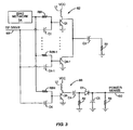
- FIG. 3 is a more detailed schematic representation of the power amplifier circuitry of the first embodiment of the present invention.
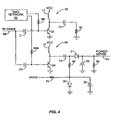
- Figure 4 is a schematic representation of power amplifier circuitry incorporating power detection circuitry according to a second embodiment of the present invention.
- Figure 5 is a schematic representation of power amplifier circuitry incorporating power detection circuitry according to a third embodiment of the present invention.
- Figure 6 is a schematic representation of power amplifier circuitry incorporating power detection circuitry according to a fourth embodiment of the present invention.
- the present invention relates to an efficient technique for detecting transmit power associated with a power amplifier.
- the technique may be implemented in numerous embodiments, several of which are discussed in detail below.
- the embodiments set forth below represent the necessary information to enable those skilled in the art to practice the invention and illustrate the best mode of practicing the invention. Upon reading the following description in light of the accompanying drawing figures, those skilled in the art will understand the concepts of the invention and will recognize applications of these concepts not particularly addressed herein.
- the present invention may be Incorporated in a mobile terminal 20, such as a mobile telephone, wireless personal digital assistant, or like communication device.
- the basic architecture of a mobile terminal 20 is represented in Figure 1 and may include a receiver front end 22, a radio frequency transmitter section 24, an antenna 26, a duplexer or switch 28, a baseband processor 30, a control system 32, a frequency synthesizer 34, and an interface 36.
- the receiver front end 22 receives information bearing radio frequency signals from one or more remote transmitters provided by a base station.
- a low noise amplifier 38 amplifies the signal.
- a filter circuit 40 minimizes broadband interference in the received signal, while downconversion and digitization circuitry 42 downconverts the filtered, received signal to an intermediate or baseband frequency signal, which is then digitized into one or more digital streams.
- the receiver front end 22 typically uses one or more mixing frequencies generated by the frequency synthesizer 34.
- the baseband processor 30 processes the digitized received signal to extract the information or data bits conveyed in the received signal. This processing typically comprises demodulation, decoding, and error correction operations. As such, the baseband processor 30 is generally implemented in one or more digital signal processors (DSPs).
- DSPs digital signal processors
- the baseband processor 30 receives digitized data, which may represent voice, data, or control information, from the control system 32, which it encodes for transmission.
- the encoded data is output to the transmitter 24, where it is used by a modulator 44 to modulate a carrier signal that is at a desired transmit frequency.
- Power amplifier circuitry 46 amplifies the modulated carrier signal to a level appropriate for transmission, and delivers the modulated carrier signal to antenna 26 through a matching network 48.
- a user may interact with the mobile terminal 20 via the interface 36, which may include interface circuitry 50 associated with a microphone 52, a speaker 54, a keypad 56, and a display 58.
- the interface circuitry 50 typically includes analog-to-digital converters, digital-to-analog converters, amplifiers, and the like. Additionally, it may include a voice encoder/decoder, in which case it may communicate directly with the baseband processor 30.
- the microphone 52 will typically convert audio input, such as the user's voice, into an electrical signal, which is then digitized and passed directly or indirectly to the baseband processor 30. Audio information encoded in the received signal is recovered by the baseband processor 30, and converted by the interface circuitry 50 into an analog signal suitable for driving speaker 54.
- the keypad 56 and display 58 enable the user to interact with the mobile terminal 20, input numbers to be dialed, address book information, or the like, as well as monitor call progress information.
- the present invention provides an efficient way to detect the transmit power provided by the power amplifier circuitry 46.
- a signal indicative of transmit power referred to as power sense (POWER SENSE) 60, is generated in the power amplifier circuitry 46 and fed back to the control system 32, which will react accordingly to control input signal levels, bias, gain, or a combination thereof in traditional fashion to control transmit power.
- POWER SENSE power sense
- a first embodiment of the present invention includes an amplifier 62, bias network 64, and detector circuitry 66.
- the detector circuitry 66 includes a transistor ON, which is a scaled version of a transistor network forming the output stage of the amplifier 62.
- the transistor network is represented by the single transistor Q1, bias resistor RB1, and coupling capacitor C1.
- the bias network is configured to deliver bias through bias resistor RB1 to the base of transistor (network) Q1.
- the radio frequency (RF) drive 68 is coupled to the base of transistor (network) Q1 through capacitor C1.
- the transistor (network) Q1 will amplify the RF drive 68 in light of the bias provided by bias network 64 to create an output signal, which is delivered through capacitor C3 to an output load R1.
- the capacitor C3 could be replaced by the output matching network 48 and the output load R1 represents the load impedance of the antenna 26.
- the transistor (network) Q1 is coupled to a voltage source (VCC) through inductor L1.
- the detector circuitry 66 is a scaled version of the amplifier 62 and is configured to include a transistor QN receiving bias from the bias network 64 through resistor RBN and RF drive 68 through capacitor CN.
- the transistor QN is coupled to voltage source VCC through inductor L2.
- the detector circuitry 66 receives the RF drive 68 and bias from the bias network 64 and creates a scaled output signal, which is a scaled version of the output signal generated by the amplifier 62, at the collector of transistor QN.
- Diode D1 rectifies the scaled output signal, and capacitor C5 and resistor R3 filter the rectified signal to create a power sense signal 60 proportional to the transmit power associated with the output signal of the amplifier 62.
- capacitor C4 and resistor R2 represent the RF load impedance for the transistor QN, and this impedance is a scaled replica of the RF load impedance presented to the transistor (network) Q1 by capacitor C3 and resistor R1.
- Capacitor C5 filters RF from the power sense signal 60, and resistor R3, the load resistance of the detector, is selected to set the level of the power sense signal 60.
- the power output capability of transistor QN of the detector network 66 is proportionally less than that of the transistor (network) Q1.
- the emitter area associated with transistor QN relates to the total emitter area of the transistor (network) Q1 by a scaling ratio A. Since the size of Q1 and QN differ by the scaling ratio A, the input and output impedances of the two transistors differ by the scaling ratio A. This in turn will cause that the RF drive 68 will be proportionally divided between the two transistors Q1 and QN. The RF drive delivered to the transistor QN will be 1/(A + 1) times the total RF drive 68.
- the bias provided to the transistor (network) Q1 and the transistor QN of the detector circuitry 66 is set such that the scaled output signal of the detector circuitry 66 relates to the output signal of the amplifier 62 by factor of A.
- the total emitter area, or device size, for transistor (network) Q1 equals A times the emitter area for transistor QN. Accordingly, capacitor C1 equals A times the capacitance of capacitor CN, and the value of resistor R1 equals the resistance of resistor R2 divided by A.
- the scaling ratio chosen is not critical, as long as the above equations are met. For example, the detector circuitry 66 has been fabricated for applications at 900 MHz and 1800 MHz, and scaling ratios of 144, 72 and 48 have been used.
- the transistor (network) Q1 and the transistor QN of the detector circuit may be provided by an array of identical transistors Q1 through QN wherein transistors Q1 through QN-1 are used in the amplifier 62 and a single transistor QN is used in the diode detector circuitry 66.
- each transistor Q1 through QN receives identical bias from the bias network 64 through resistors RB1 through RBN and RF drive 68 through capacitors C1 through CN.
- the collectors of transistors Q1 through QN-1 are coupled together to provide a common output signal to capacitor C3 and load R1, which represent the matching network 48 and the load of antenna 26.
- the collector of transistor QN is coupled to capacitor C4 of the detector circuitry 66 instead of the other collectors of transistors Q1 through QN-1.
- the signals at the collectors of transistors Q1 through QN-1 are combined to form an output signal A times that of the scaled output signal provided by transistor QN, assuming that A equals one less than the total number of transistors, or N-1.
- the transistors Q1 through QN are preferably heterojunction bipolar transistors (HBTs) formed on a single semiconductor and equally sized to form a transistor array.
- HBTs heterojunction bipolar transistors
- the inventive concepts defined herein are independent of technology (Si, GaAs, SiGe, etc.) as well as device type (BJT, FET, MESFET, HBT, etc.).
- the technology in which the invention is implement should have both amplifying elements and a detector element, such as diode D1.
- the amplifying elements are GaAs HBT devices
- the detector element is a GaAs Schottky diode.
- Patent Application Number 09/467,415 entitled BIAS NETWORK FOR HIGH EFFICIENCY RF LINEAR POWER AMPLIFIER, filed December 20,1999, currently pending, the disclosure of which is incorporated herein by reference in its entirety. Upon understanding the present invention, those skilled in the art will be able to construct any number of bias networks that are compatible with the present invention.
- diode D1 In order to improve the low power performance and dynamic range of the detector circuitry 66, a small amount of bias current can be applied to diode D1.
- An exemplary embodiment is illustrated in Figure 4.
- the anode of diode D2 is connected to resistor R2.
- the cathode of diode D2 is connected to ground.
- a regulated voltage (VREG) is provided to drive resistor R4 to provide current through diode D2, which establishes the voltage appearing at the anode of D2.
- diode D2 functions as a voltage source from which a variable amount of DC current may be drawn by the rectifier diode D1.
- resistor R4 and diode D2 may by selected such that approximately 15 ⁇ A of current flow through D1 with no RF present in the circuit.
- the size of the diode D2 may be adjusted in order to adjust the voltage appearing at the anode of D2.
- diode D2 may be composed of 8 or 16 parallel diodes. The paralleling of many diodes lowers the voltage appearing at the anode of diode D2.
- the voltage at the anode of diode D2 is between 0.5 V and 0.6 V. Approximately 1 mA of quiescent current flows through resistor R4 and diode D2 to ground.
- diode voltage source to supply the bias current for the rectifier diode D1 provides temperature and process stability to reduce circuit performance variations due to temperature and diode manufacturing process variations. At higher temperatures, the diode potential drop from anode to cathode for a given diode current decreases. If the bias voltage source, represented by diode D2, were instead a constant voltage source not varying with temperature, then an increase in temperature would result in an increase in the DC voltage appearing at R3 (all other things being equal), since the voltage at R3 is equal to the voltage at D2 minus the potential drop across R2 and D1.
- Capacitor C6 is an RF bypass used to ensure that the RF load impedance of QN, represented by resistor R2, does not substantially change with the addition of the bias circuitry R4 and D2.
- resistor R5 is added in series with resistor R4, and diodes D3 and D4 are coupled between resistors R4 and R5 and ground.
- the voltage drop across diodes D3 and D4 remains stable as VREG varies, thus causing the voltage at the anode of diode D2 to remain more constant as VREG varies.
- Another circuit modification is directed to reduce variations resulting from the voltage at the anode of diode D2 varying as a function of the RF power detected.
- the DC current flowing through resistor R2 diode D1 and resistor R3 likewise increases because diode D1 is rectifying the AC signal appearing at the anode of diode D1.
- the power sense signal 60 voltage appearing at resistor R3 increases as the RF power delivered to resistor R2 increases. Since diode D2 is acting as the voltage source from which the DC current is supplied, and since diode D2 is not an ideal voltage source, when additional DC current is drawn, the voltage across D2 collapses slightly.
- diodes D5 and D6 function as a nonlinear resistance, the value of the resistance decreasing with increasing current flow through the diodes, and this keeps the voltage at diode D2 more stable as a function of the variable current drawn from the diode D2 source, which fluctuates as a function of the RF power delivered to resistor R2.
- the current drawn from the diode D2 source may vary from 15 ⁇ A with no RF present at resistor R2 to approximately 300-500 ⁇ A with maximum RF present at resistor R2, which is approximately 15 dBm.
- the circuit shown in Figure 6 has achieved accuracy better than +/- 0.2 dB.
- VREG is nominally 2.75 volts
- the voltage across resistor R3 may vary from 50 mV with no RF present at resistor R2 to approximately 2.2 volts with 15 dBm present at resistor R2.
- the output signal delivered to the load R1 is typically between 31 dBm to 34 dBm.
Landscapes
- Engineering & Computer Science (AREA)
- Power Engineering (AREA)
- Amplifiers (AREA)
- Transmitters (AREA)
Applications Claiming Priority (3)
| Application Number | Priority Date | Filing Date | Title |
|---|---|---|---|
| US09/952,524 US7190935B2 (en) | 2001-09-14 | 2001-09-14 | Amplifier power detection circuitry |
| US952524 | 2001-09-14 | ||
| PCT/US2002/028622 WO2003026333A1 (en) | 2001-09-14 | 2002-09-10 | Amplifier power detection circuitry |
Publications (2)
| Publication Number | Publication Date |
|---|---|
| EP1437023A1 EP1437023A1 (en) | 2004-07-14 |
| EP1437023B1 true EP1437023B1 (en) | 2006-04-19 |
Family
ID=25492989
Family Applications (1)
| Application Number | Title | Priority Date | Filing Date |
|---|---|---|---|
| EP02798939A Expired - Lifetime EP1437023B1 (en) | 2001-09-14 | 2002-09-10 | Amplifier power detection circuitry |
Country Status (5)
| Country | Link |
|---|---|
| US (1) | US7190935B2 (enExample) |
| EP (1) | EP1437023B1 (enExample) |
| JP (1) | JP4139329B2 (enExample) |
| DE (1) | DE60210796T2 (enExample) |
| WO (1) | WO2003026333A1 (enExample) |
Families Citing this family (30)
| Publication number | Priority date | Publication date | Assignee | Title |
|---|---|---|---|---|
| US6701138B2 (en) * | 2001-06-11 | 2004-03-02 | Rf Micro Devices, Inc. | Power amplifier control |
| US6957092B2 (en) * | 2002-12-30 | 2005-10-18 | Motorola, Inc. | Disposable device with removable radio module |
| US7010330B1 (en) | 2003-03-01 | 2006-03-07 | Theta Microelectronics, Inc. | Power dissipation reduction in wireless transceivers |
| US6969978B2 (en) * | 2003-03-17 | 2005-11-29 | Rf Micro Devices, Inc. | DC-DC converter with reduced electromagnetic interference |
| US20050032499A1 (en) * | 2003-08-08 | 2005-02-10 | Cho Jin Wook | Radio frequency power detecting circuit and method therefor |
| US20050037716A1 (en) * | 2003-08-12 | 2005-02-17 | Motorola, Inc. | Apparatus and method for wideband integrated radio frequency detection |
| US6998919B2 (en) * | 2003-10-22 | 2006-02-14 | Rf Micro Devices, Inc. | Temperature compensated power amplifier power control |
| US6980039B1 (en) | 2004-03-03 | 2005-12-27 | Rf Micro Devices, Inc. | DC-DC converter with noise spreading to meet spectral mask requirements |
| US7053713B1 (en) | 2004-06-02 | 2006-05-30 | Rf Micro Devices, Inc. | Multi-phase switching power supply having both voltage and current feedback loops |
| US7301400B1 (en) | 2004-06-02 | 2007-11-27 | Rf Micro Devices, Inc. | Multi-phase switching power supply for mobile telephone applications |
| US7193459B1 (en) | 2004-06-23 | 2007-03-20 | Rf Micro Devices, Inc. | Power amplifier control technique for enhanced efficiency |
| US7109791B1 (en) | 2004-07-09 | 2006-09-19 | Rf Micro Devices, Inc. | Tailored collector voltage to minimize variation in AM to PM distortion in a power amplifier |
| WO2006018784A2 (en) * | 2004-08-16 | 2006-02-23 | Koninklijke Philips Electronics N.V. | High accuracy power detector for handset applications |
| US7132891B1 (en) | 2004-08-17 | 2006-11-07 | Rf Micro Devices, Inc. | Power amplifier control using a switching power supply |
| US7340235B1 (en) * | 2004-08-20 | 2008-03-04 | Rf Micro Devices, Inc. | System for limiting current in an output stage of a power amplifier |
| US7167054B1 (en) | 2004-12-02 | 2007-01-23 | Rf Micro Devices, Inc. | Reconfigurable power control for a mobile terminal |
| US7256650B1 (en) | 2005-02-28 | 2007-08-14 | Rf Micro Devices, Inc. | VSWR tolerant power detector |
| US7336127B2 (en) * | 2005-06-10 | 2008-02-26 | Rf Micro Devices, Inc. | Doherty amplifier configuration for a collector controlled power amplifier |
| US7671684B2 (en) * | 2005-07-05 | 2010-03-02 | Japan Radio Co., Ltd. | FET bias circuit |
| US8700093B2 (en) * | 2005-09-26 | 2014-04-15 | 8631654 Canada Inc. | Wireless communication base station with current limiting capability |
| US20070071047A1 (en) * | 2005-09-29 | 2007-03-29 | Cymer, Inc. | 6K pulse repetition rate and above gas discharge laser system solid state pulse power system improvements |
| US7330071B1 (en) | 2005-10-19 | 2008-02-12 | Rf Micro Devices, Inc. | High efficiency radio frequency power amplifier having an extended dynamic range |
| US7551027B2 (en) * | 2007-03-09 | 2009-06-23 | Tri Quint Semiconductor, Inc. | RF power amplifier mirror circuit for sensing current |
| JP4685836B2 (ja) * | 2007-05-28 | 2011-05-18 | パナソニック株式会社 | 高周波電力増幅器 |
| US7852063B2 (en) * | 2008-06-04 | 2010-12-14 | Silicon Storage Technology, Inc. | Integrated power detector with temperature compensation for fully-closed loop control |
| US8027648B2 (en) * | 2009-04-29 | 2011-09-27 | Lockheed Martin Corporation | Radio frequency power monitor |
| JP2011030110A (ja) * | 2009-07-28 | 2011-02-10 | Panasonic Corp | 半導体装置およびそれを用いた高周波スイッチ並びに高周波モジュール |
| CN107110898B (zh) * | 2014-12-22 | 2022-06-07 | 美高森美公司 | 对数线性功率检测器 |
| US12273072B2 (en) * | 2021-12-29 | 2025-04-08 | Qualcomm Incorporated | Envelope detector with clamping circuitry |
| CN118473336B (zh) * | 2024-07-15 | 2024-10-11 | 苏州悉芯射频微电子有限公司 | 一种应用于功率放大器的功率检测器 |
Family Cites Families (31)
| Publication number | Priority date | Publication date | Assignee | Title |
|---|---|---|---|---|
| US3109992A (en) * | 1958-01-23 | 1963-11-05 | Collins Radio Co | Temperature-stabilized and distortionless diode detector |
| US3449680A (en) * | 1966-03-29 | 1969-06-10 | Motorola Inc | Transistor protection circuit |
| US4122400A (en) * | 1976-11-08 | 1978-10-24 | Rca Corporation | Amplifier protection circuit |
| US4233474A (en) * | 1978-01-10 | 1980-11-11 | Nippon Electric Co., Ltd. | Telephone transmitter amplifier |
| US4523155A (en) * | 1983-05-04 | 1985-06-11 | Motorola, Inc. | Temperature compensated automatic output control circuitry for RF signal power amplifiers with wide dynamic range |
| US4924194A (en) * | 1989-05-19 | 1990-05-08 | Motorola, Inc. | RF power amplifier |
| JPH03258121A (ja) * | 1990-03-08 | 1991-11-18 | Oki Electric Ind Co Ltd | 検波回路 |
| US5126688A (en) * | 1990-03-20 | 1992-06-30 | Oki Electric Co., Ltd. | Power amplifying apparatus for wireless transmitter |
| JPH0423506A (ja) * | 1990-05-17 | 1992-01-27 | Nec Corp | Agc検波回路 |
| JPH0440105A (ja) * | 1990-06-06 | 1992-02-10 | Oki Electric Ind Co Ltd | 線形化増幅回路 |
| KR960000775B1 (ko) * | 1990-10-19 | 1996-01-12 | 닛본덴기 가부시끼가이샤 | 고주파 전력 증폭기의 출력레벨 제어회로 |
| TW225619B (enExample) * | 1991-07-19 | 1994-06-21 | Nippon Electric Co | |
| US5204614A (en) | 1991-08-14 | 1993-04-20 | Hewlett-Packard Company | Broad-band microwave power sensor using diodes above their resonant frequency |
| JPH06177780A (ja) * | 1992-12-07 | 1994-06-24 | Uniden Corp | 送信出力安定回路 |
| US5608353A (en) * | 1995-03-29 | 1997-03-04 | Rf Micro Devices, Inc. | HBT power amplifier |
| JP3223750B2 (ja) * | 1995-03-31 | 2001-10-29 | 株式会社日立製作所 | 出力制御電力増幅器、無線通信端末及び無線通信基地局 |
| US5678209A (en) * | 1995-03-31 | 1997-10-14 | Lucent Technologies Inc. | Transmit power level detection circuit with enhanced gain characteristics |
| US6434374B1 (en) * | 1996-03-29 | 2002-08-13 | Thomson Licensing S.A. | Apparatus for controlling the conversion gain of a down converter |
| JP3093638B2 (ja) * | 1996-06-18 | 2000-10-03 | 埼玉日本電気株式会社 | 出力レベル制御回路 |
| GB2318004A (en) * | 1996-10-01 | 1998-04-08 | Nokia Mobile Phones Ltd | A diode detector |
| US5923153A (en) * | 1997-02-24 | 1999-07-13 | Lucent Technologies Inc. | Circuit for moderating a peak reverse recovery current of a rectifier and method of operation thereof |
| US5956627A (en) * | 1997-07-08 | 1999-09-21 | Uniden San Diego Research & Development Center, Inc. | Temperature compensated power control circuit |
| US6108527A (en) * | 1997-07-31 | 2000-08-22 | Lucent Technologies, Inc. | Wide range multiple band RF power detector |
| US6272336B1 (en) * | 1998-12-30 | 2001-08-07 | Samsung Electronics Co., Ltd. | Traffic-weighted closed loop power detection system for use with an RF power amplifier and method of operation |
| JP3235580B2 (ja) * | 1999-01-08 | 2001-12-04 | 日本電気株式会社 | 高効率増幅器 |
| US6262630B1 (en) * | 1999-06-04 | 2001-07-17 | Telefonaktiebolaget Lm Ericsson (Publ) | Rapidly-responding diode detector with temperature compensation |
| US6307364B1 (en) * | 1999-08-27 | 2001-10-23 | Rf Micro Devices, Inc. | Power sensor for RF power amplifier |
| US6211735B1 (en) * | 2000-01-21 | 2001-04-03 | Harris Corporation | RF power amplifier having improved power supply for RF drive circuits |
| US6265943B1 (en) | 2000-01-27 | 2001-07-24 | Rf Micro Devices, Inc. | Integrated RF power sensor that compensates for bias changes |
| US6624702B1 (en) * | 2002-04-05 | 2003-09-23 | Rf Micro Devices, Inc. | Automatic Vcc control for optimum power amplifier efficiency |
| US6822515B2 (en) * | 2002-07-19 | 2004-11-23 | Ikuroh Ichitsubo | Accurate power sensing circuit for power amplifiers |
-
2001
- 2001-09-14 US US09/952,524 patent/US7190935B2/en not_active Expired - Lifetime
-
2002
- 2002-09-10 JP JP2003529795A patent/JP4139329B2/ja not_active Expired - Fee Related
- 2002-09-10 WO PCT/US2002/028622 patent/WO2003026333A1/en not_active Ceased
- 2002-09-10 DE DE60210796T patent/DE60210796T2/de not_active Expired - Lifetime
- 2002-09-10 EP EP02798939A patent/EP1437023B1/en not_active Expired - Lifetime
Also Published As
| Publication number | Publication date |
|---|---|
| WO2003026333A1 (en) | 2003-03-27 |
| US20030054778A1 (en) | 2003-03-20 |
| EP1437023A1 (en) | 2004-07-14 |
| US7190935B2 (en) | 2007-03-13 |
| JP4139329B2 (ja) | 2008-08-27 |
| JP2005528001A (ja) | 2005-09-15 |
| DE60210796T2 (de) | 2006-12-28 |
| DE60210796D1 (de) | 2006-05-24 |
Similar Documents
| Publication | Publication Date | Title |
|---|---|---|
| EP1437023B1 (en) | Amplifier power detection circuitry | |
| US5559471A (en) | Amplifier and biasing circuit therefor | |
| US6701138B2 (en) | Power amplifier control | |
| US7193459B1 (en) | Power amplifier control technique for enhanced efficiency | |
| JP3079095B2 (ja) | 移動通信端末機の電源供給方法及びその装置 | |
| US6285239B1 (en) | Feed-forward biasing for RF amplifiers | |
| US6972628B2 (en) | Integratable, voltage-controlled RF power amplifier | |
| US5796309A (en) | Temperature compensated wide dynamic range power detection circuitry for portable RF transmission terminals | |
| EP1897216B1 (en) | Automatic bias control circuit for linear power amplifiers | |
| US6839549B2 (en) | System and method of RF power amplification | |
| US6850119B2 (en) | Power amplifier overload protection | |
| US20050032499A1 (en) | Radio frequency power detecting circuit and method therefor | |
| US7772927B1 (en) | Active bias Darlington amplifier | |
| WO1999067893A1 (en) | Dual band cellular phone with two power amplifiers and power control circuit therefor | |
| US7256650B1 (en) | VSWR tolerant power detector | |
| EP1800395B1 (en) | Dual bias control circuit | |
| US7454179B1 (en) | Radio frequency power detector and decision circuit used with DC supply voltage controlled power amplifiers | |
| GB2440772A (en) | A power supply modulator for an RF amplifier | |
| CN1075286C (zh) | 功率放大器电路 | |
| US7440734B1 (en) | Active quadrature radio frequency power detector | |
| US20040070454A1 (en) | Continuous bias circuit and method for an amplifier | |
| WO2006018784A2 (en) | High accuracy power detector for handset applications |
Legal Events
| Date | Code | Title | Description |
|---|---|---|---|
| PUAI | Public reference made under article 153(3) epc to a published international application that has entered the european phase |
Free format text: ORIGINAL CODE: 0009012 |
|
| 17P | Request for examination filed |
Effective date: 20040316 |
|
| AK | Designated contracting states |
Kind code of ref document: A1 Designated state(s): AT BE BG CH CY CZ DE DK EE ES FI FR GB GR IE IT LI LU MC NL PT SE SK TR |
|
| AX | Request for extension of the european patent |
Extension state: AL LT LV MK RO SI |
|
| 17Q | First examination report despatched |
Effective date: 20041126 |
|
| GRAP | Despatch of communication of intention to grant a patent |
Free format text: ORIGINAL CODE: EPIDOSNIGR1 |
|
| GRAS | Grant fee paid |
Free format text: ORIGINAL CODE: EPIDOSNIGR3 |
|
| GRAA | (expected) grant |
Free format text: ORIGINAL CODE: 0009210 |
|
| AK | Designated contracting states |
Kind code of ref document: B1 Designated state(s): DE FR GB |
|
| REG | Reference to a national code |
Ref country code: GB Ref legal event code: FG4D |
|
| REF | Corresponds to: |
Ref document number: 60210796 Country of ref document: DE Date of ref document: 20060524 Kind code of ref document: P |
|
| ET | Fr: translation filed | ||
| PLBE | No opposition filed within time limit |
Free format text: ORIGINAL CODE: 0009261 |
|
| STAA | Information on the status of an ep patent application or granted ep patent |
Free format text: STATUS: NO OPPOSITION FILED WITHIN TIME LIMIT |
|
| 26N | No opposition filed |
Effective date: 20070122 |
|
| REG | Reference to a national code |
Ref country code: FR Ref legal event code: PLFP Year of fee payment: 15 |
|
| PGFP | Annual fee paid to national office [announced via postgrant information from national office to epo] |
Ref country code: DE Payment date: 20160907 Year of fee payment: 15 Ref country code: GB Payment date: 20160907 Year of fee payment: 15 |
|
| PGFP | Annual fee paid to national office [announced via postgrant information from national office to epo] |
Ref country code: FR Payment date: 20160816 Year of fee payment: 15 |
|
| REG | Reference to a national code |
Ref country code: DE Ref legal event code: R119 Ref document number: 60210796 Country of ref document: DE |
|
| GBPC | Gb: european patent ceased through non-payment of renewal fee |
Effective date: 20170910 |
|
| REG | Reference to a national code |
Ref country code: FR Ref legal event code: ST Effective date: 20180531 |
|
| PG25 | Lapsed in a contracting state [announced via postgrant information from national office to epo] |
Ref country code: GB Free format text: LAPSE BECAUSE OF NON-PAYMENT OF DUE FEES Effective date: 20170910 Ref country code: DE Free format text: LAPSE BECAUSE OF NON-PAYMENT OF DUE FEES Effective date: 20180404 |
|
| PG25 | Lapsed in a contracting state [announced via postgrant information from national office to epo] |
Ref country code: FR Free format text: LAPSE BECAUSE OF NON-PAYMENT OF DUE FEES Effective date: 20171002 |