EP1434276A2 - Angepasster Bildsensor für eine Packung in Chip-Grösse - Google Patents
Angepasster Bildsensor für eine Packung in Chip-Grösse Download PDFInfo
- Publication number
- EP1434276A2 EP1434276A2 EP03256671A EP03256671A EP1434276A2 EP 1434276 A2 EP1434276 A2 EP 1434276A2 EP 03256671 A EP03256671 A EP 03256671A EP 03256671 A EP03256671 A EP 03256671A EP 1434276 A2 EP1434276 A2 EP 1434276A2
- Authority
- EP
- European Patent Office
- Prior art keywords
- image sensor
- sensor die
- spacer ring
- die
- stack bumps
- Prior art date
- Legal status (The legal status is an assumption and is not a legal conclusion. Google has not performed a legal analysis and makes no representation as to the accuracy of the status listed.)
- Granted
Links
Images


Classifications
-
- H—ELECTRICITY
- H10—SEMICONDUCTOR DEVICES; ELECTRIC SOLID-STATE DEVICES NOT OTHERWISE PROVIDED FOR
- H10F—INORGANIC SEMICONDUCTOR DEVICES SENSITIVE TO INFRARED RADIATION, LIGHT, ELECTROMAGNETIC RADIATION OF SHORTER WAVELENGTH OR CORPUSCULAR RADIATION
- H10F39/00—Integrated devices, or assemblies of multiple devices, comprising at least one element covered by group H10F30/00, e.g. radiation detectors comprising photodiode arrays
- H10F39/80—Constructional details of image sensors
- H10F39/804—Containers or encapsulations
Definitions
- the present invention is related to image sensing integrated circuits, and more particularly, to a simplified chip scale package for image sensors.
- Image sensors are now extensively used in many applications ranging from cell phone cameras, PC cameras, digital still cameras, and security cameras. Most of these applications require that the image sensor withstand varying environmental conditions. Because of this, chip package solutions for image sensors have been developed to protect the image sensor from environmental factors.
- FIG. 1 A prior art structure is shown in Figure 1 in exploded isometric view.
- Figure 2 shows the structure of Figure 1 in assembled cross-section view.
- the chip package includes a substrate 101 that has incorporated a lead frame.
- the image sensor 103 is adhered to the substrate 101.
- the lead frame is then wire bonded to contact pads on the image sensor 103.
- a cap or spacer 105 is then secured to the lead frame in order to provide spacing between a glass lid 107 and the image sensor 103.
- the glass lid 107 is required to allow transparent optical imaging by the image sensor 103 to the outside world. Additionally, the glass lid 107 and the spacer 105 serve to prevent environmental contaminants from affecting the operation of the image sensor 103.
- the lead frame/substrate 101 provides a means by which signals can be read out from the image sensor 103.
- the substrate is a ceramic substrate and thus referred to as a ceramic package.
- Examples of various types of packaging techniques for image sensor are shown in U.S. Patent Application Publication No. 2002/0079438 to Lin, U.S. Patent Application Publication No. 2002/0140072 to Chiu, U.S. Patent Application Publication No. 2002/0148946 to Tu et al., and U.S. Patent Application Publication No. 2002/0006687 to Lam.
- multiple components are required to mount the image sensor onto a substrate and protect the image sensor with a glass lid.
- the present invention provides an image sensor according to Claim 1.
- Figure 1 is a prior art chip scale packaging technique for image sensor integrated circuits.
- Figure 2 is a cross-section view of the prior art structure of Figure 1 that has been assembled.
- Figure 3 is a top view of an image sensor die formed in accordance with the prior art.
- Figure 4 is a cross-section of the image sensor die of Figure 3 taken along line A-A'.
- Figure 5 is a top view of an image sensor die formed in accordance with the present invention.
- Figure 6 is a cross-section of the image sensor die of Figure 5 taken along line B-B'.
- Figure 7 is an image sensor die formed in accordance with the present invention with a glass lid attached.
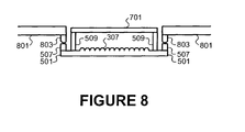
- Figure 8 shows an image sensor die of the present invention mounted onto a flexible tape.
- an image sensor is formed that includes structures on the image sensor die that aid in simplifying the packaging of the image sensor die.
- Figure 3 shows a prior art image sensor die 301 that includes a pixel array 303 and a signal processing block 305. Both the pixel array 303 and the signal processing block 305 are formed on the die 301.
- Other circuitry (such as input/output buffers, drivers, and other components) are typically present on the die 301, but are not shown to avoid obscuring the present invention.
- the image sensor die 301 includes microlenses 307 that are formed atop of each pixel in the pixel array.
- the microlenses 307 are present to aid in increasing the fill factor of each pixel.
- bonding pads 302 are formed into the substrate of the die 301.
- the bonding pads 302 are also referred to as contact pads and are used for wire bonding the image sensor die 301 to the lead frame 101 of Figure 1.
- the prior art image sensor die 301 of Figures 3 and 4 requires the multiple component chip scale package shown in Figures 1 and 2. As noted earlier, because of the multiple components required to package this image sensor die 301, the cost is relatively high.
- Figures 5 and 6 illustrate an image sensor die formed in accordance with the present invention.
- the core areas of the die 501 remain the same, i.e., the pixel array 503 and the signal processing block remain as in the prior art.
- the structure of the pixel area 503, the signal processing block, and other circuit structures are well known in the art.
- OmniVision Technologies, Inc. is the owner of several patents detailing the formation of an image sensor die, those patents be incorporated by reference in their entirety.
- the present invention is directed towards modifying those prior art image sensor dies with additional structures in order to more efficiently provide chip scale packaging.
- stack bumps 507 are present along the peripheral regions of the die 501.
- the stack bumps 507 are typically formed from a conductive material, such as aluminum, tungsten, copper, titanium, or the like. In one embodiment, the stack bumps 507 are formed by a deposition and etch process. However, other methods for forming the stack bumps 507 are suitable. In one embodiment, the stack bumps 507 are raised above the surface of the image sensor die, and typically raised well above the surface of the microlenses 307. The stack bumps 507 serve to propagate signals output by the image sensor die 501 to either a printed circuit board or other packaging system. Therefore, the stack bumps 507 can be directly attached to a printed circuit board, similar to a ball grid array (BGA) connection technique.
- BGA ball grid array
- a spacer ring 509 is formed around the pixel array 503.
- the purpose of the spacer ring 509 is to support a glass lid 701 (see Figure 7) that will form a seal and protect the pixel array 503.
- the term glass lid as used herein is not limited to a glass material, but refers to any material that is substantially transparent to radiation having a selected wavelength.
- the spacer ring 509 extends around the entire periphery of the image sensor die 501, encompassing nearly all of the circuitry except for the stack bumps 507.
- the spacer ring 507 only surrounds the pixel array 503 and the glass lid 701 is sized to coincide with the shape of the spacer ring 509.
- the material used to form the spacer ring is variable, but preferably should not be a conducting material.
- the material to form the spacer ring 509 should be easily formed onto an image sensor die 501 using conventional semiconductor processes.
- an oxide or other dielectric material may be used.
- the formation of the spacer ring 509 can be performed using conventional semiconductor techniques including deposition, masking, and etching. Alternatively, the spacer ring 509 can be formed by direct printing or dispensing.
- the spacer ring 509 should extend above the microlenses 307 such that the glass lid 701 is not in contact with the microlenses 307.
- the spacer ring 509 is shown to be taller than the stack bumps 507, in other embodiments, the spacer ring 509 has a lesser height than the stack bumps 507.
- the spacer ring 509 Other types of materials suitable for use for the spacer ring 509 are epoxies, polyimides, or resins.
- the advantage of an epoxy is that the glass lid 701 can be secured directly to the spacer ring 509.
- the glass lid 701 may be secured to the spacer ring 509 either prior to or after the image sensor die 501 have been diced into individual units out of the wafer.
- the glass lid 701 is secured to the individual image sensor die 501 prior to dicing. This has the advantage of minimizing or eliminating particulate contamination of the pixel array during the dicing process.
- a flexible tape 801 includes connectors 803 that can be electrically attached to the stack bumps 507, by any number of conventional means. Further, although a flexible tape 801 is shown, a printed circuit board can easily be substituted therefore.
- the present invention discloses an image sensor die that has structures intended to more efficiently package the image sensor die.
- the structures include a spacer ring and stack bumps.
- the spacer ring serves to support a glass lid over the pixel array of the image sensor die.
- the stack bumbs are raised in order to facilitate direct connection to flexible tape or a printed circuit board.
- a method for forming image sensor dies comprises forming a plurality of image sensor dies onto a semiconductor wafer.
- the image sensor die include a spacer ring structure and stack bumps. Glass lids are placed onto the spacer ring to seal and protect the pixel array.
- the wafer is then diced into individual image sensor die. Following dicing, the individual image sensor die are then packaged further by attaching, through the stack bumps, to a flexible tape or a printed circuit board, or in fact any other type of structural apparatus.
Landscapes
- Solid State Image Pick-Up Elements (AREA)
- Transforming Light Signals Into Electric Signals (AREA)
- Studio Devices (AREA)
- Apparatus For Radiation Diagnosis (AREA)
Applications Claiming Priority (2)
| Application Number | Priority Date | Filing Date | Title |
|---|---|---|---|
| US330824 | 2002-12-26 | ||
| US10/330,824 US20040124486A1 (en) | 2002-12-26 | 2002-12-26 | Image sensor adapted for reduced component chip scale packaging |
Publications (3)
| Publication Number | Publication Date |
|---|---|
| EP1434276A2 true EP1434276A2 (de) | 2004-06-30 |
| EP1434276A3 EP1434276A3 (de) | 2004-07-14 |
| EP1434276B1 EP1434276B1 (de) | 2009-07-01 |
Family
ID=32469049
Family Applications (1)
| Application Number | Title | Priority Date | Filing Date |
|---|---|---|---|
| EP03256671A Expired - Lifetime EP1434276B1 (de) | 2002-12-26 | 2003-10-23 | Angepasster Bildsensor für eine Packung in Chip-Grösse |
Country Status (6)
| Country | Link |
|---|---|
| US (1) | US20040124486A1 (de) |
| EP (1) | EP1434276B1 (de) |
| CN (1) | CN100373628C (de) |
| AT (1) | ATE435503T1 (de) |
| DE (1) | DE60328159D1 (de) |
| TW (1) | TWI240409B (de) |
Cited By (1)
| Publication number | Priority date | Publication date | Assignee | Title |
|---|---|---|---|---|
| CN101369591B (zh) * | 2007-08-17 | 2010-07-07 | 精材科技股份有限公司 | 影像感测元件封装体及其制作方法 |
Families Citing this family (8)
| Publication number | Priority date | Publication date | Assignee | Title |
|---|---|---|---|---|
| US7365442B2 (en) * | 2003-03-31 | 2008-04-29 | Osram Opto Semiconductors Gmbh | Encapsulation of thin-film electronic devices |
| JP4551638B2 (ja) * | 2003-08-01 | 2010-09-29 | 富士フイルム株式会社 | 固体撮像装置の製造方法 |
| JP2005056998A (ja) * | 2003-08-01 | 2005-03-03 | Fuji Photo Film Co Ltd | 固体撮像装置およびその製造方法 |
| US7288757B2 (en) | 2005-09-01 | 2007-10-30 | Micron Technology, Inc. | Microelectronic imaging devices and associated methods for attaching transmissive elements |
| JP2007142042A (ja) * | 2005-11-16 | 2007-06-07 | Sharp Corp | 半導体パッケージとその製造方法,半導体モジュール,および電子機器 |
| CN101627450B (zh) * | 2007-03-08 | 2013-10-30 | 日本电气株式会社 | 电容元件、印刷布线板、半导体封装以及半导体电路 |
| KR101711007B1 (ko) | 2010-04-29 | 2017-03-02 | 삼성전자주식회사 | 이미지 센서 패키지를 갖는 이미지 센서 모듈 |
| JP2018093290A (ja) * | 2016-11-30 | 2018-06-14 | キヤノン・コンポーネンツ株式会社 | イメージセンサユニット、画像読取装置および画像形成装置 |
Citations (3)
| Publication number | Priority date | Publication date | Assignee | Title |
|---|---|---|---|---|
| JPH11121653A (ja) | 1997-07-31 | 1999-04-30 | Fuji Film Microdevices Co Ltd | 半導体装置とその製造方法 |
| EP1041628A2 (de) | 1999-03-29 | 2000-10-04 | Interuniversitair Microelektronica Centrum Vzw | BGA-Bildsensor-Verpackung und deren Herstellungsmethode |
| US6285064B1 (en) | 2000-03-28 | 2001-09-04 | Omnivision Technologies, Inc. | Chip scale packaging technique for optical image sensing integrated circuits |
Family Cites Families (6)
| Publication number | Priority date | Publication date | Assignee | Title |
|---|---|---|---|---|
| JPH09232551A (ja) * | 1996-02-26 | 1997-09-05 | Toshiba Corp | 光電変換装置 |
| US6037609A (en) * | 1997-01-17 | 2000-03-14 | General Electric Company | Corrosion resistant imager |
| WO2001061994A1 (en) * | 2000-02-18 | 2001-08-23 | Intelligent Pixels, Inc. | Very low-power parallel video processor pixel circuit |
| US6396116B1 (en) * | 2000-02-25 | 2002-05-28 | Agilent Technologies, Inc. | Integrated circuit packaging for optical sensor devices |
| TW454323B (en) * | 2000-08-10 | 2001-09-11 | Uincent Lin | Image sensor package structure and substrate thereof |
| US20030111588A1 (en) * | 2001-12-18 | 2003-06-19 | Pao-Jung Chen | Near-contact optical touch-screen sensor module |
-
2002
- 2002-12-26 US US10/330,824 patent/US20040124486A1/en not_active Abandoned
-
2003
- 2003-10-09 TW TW092128199A patent/TWI240409B/zh not_active IP Right Cessation
- 2003-10-23 EP EP03256671A patent/EP1434276B1/de not_active Expired - Lifetime
- 2003-10-23 AT AT03256671T patent/ATE435503T1/de not_active IP Right Cessation
- 2003-10-23 DE DE60328159T patent/DE60328159D1/de not_active Expired - Lifetime
- 2003-10-24 CN CNB2003101043720A patent/CN100373628C/zh not_active Expired - Lifetime
Patent Citations (3)
| Publication number | Priority date | Publication date | Assignee | Title |
|---|---|---|---|---|
| JPH11121653A (ja) | 1997-07-31 | 1999-04-30 | Fuji Film Microdevices Co Ltd | 半導体装置とその製造方法 |
| EP1041628A2 (de) | 1999-03-29 | 2000-10-04 | Interuniversitair Microelektronica Centrum Vzw | BGA-Bildsensor-Verpackung und deren Herstellungsmethode |
| US6285064B1 (en) | 2000-03-28 | 2001-09-04 | Omnivision Technologies, Inc. | Chip scale packaging technique for optical image sensing integrated circuits |
Non-Patent Citations (1)
| Title |
|---|
| LU B ET AL.: "Active Pixel Sensor (APS) Package", PROCEEDINGS OF THE SPIE, vol. 3830, 1999, pages 175 - 178, XP000980682 |
Cited By (1)
| Publication number | Priority date | Publication date | Assignee | Title |
|---|---|---|---|---|
| CN101369591B (zh) * | 2007-08-17 | 2010-07-07 | 精材科技股份有限公司 | 影像感测元件封装体及其制作方法 |
Also Published As
| Publication number | Publication date |
|---|---|
| CN1512593A (zh) | 2004-07-14 |
| DE60328159D1 (de) | 2009-08-13 |
| CN100373628C (zh) | 2008-03-05 |
| TW200514243A (en) | 2005-04-16 |
| EP1434276B1 (de) | 2009-07-01 |
| ATE435503T1 (de) | 2009-07-15 |
| TWI240409B (en) | 2005-09-21 |
| EP1434276A3 (de) | 2004-07-14 |
| US20040124486A1 (en) | 2004-07-01 |
Similar Documents
| Publication | Publication Date | Title |
|---|---|---|
| US6627983B2 (en) | Stacked package structure of image sensor | |
| US6559539B2 (en) | Stacked package structure of image sensor | |
| US7321455B2 (en) | Microelectronic devices and methods for packaging microelectronic devices | |
| EP2393116B1 (de) | Waferlevel-Bildsensorverpackungsstruktur und Herstellungsverfahren dafür | |
| US6737292B2 (en) | Method of fabricating an image sensor module at the wafer level and mounting on circuit board | |
| US7929033B2 (en) | Image sensor package and camera module having same | |
| US20050099532A1 (en) | Image pickup device and a manufacturing method thereof | |
| US6933493B2 (en) | Image sensor having a photosensitive chip mounted to a metal sheet | |
| US20060091488A1 (en) | Image sensor chip package and method of fabricating the same | |
| US20040238909A1 (en) | Packaged microelectronic devices and methods of packaging microelectronic devices | |
| US20020096731A1 (en) | Package structure of an image sensor and method for packaging the same | |
| US7405100B1 (en) | Packaging of a semiconductor device with a non-opaque cover | |
| US7888157B2 (en) | Image sensor chip package method | |
| JP2008167426A (ja) | イメージセンサ・モジュール | |
| EP1434276B1 (de) | Angepasster Bildsensor für eine Packung in Chip-Grösse | |
| US20060098244A1 (en) | Image sensor assembly and method for fabricating the same | |
| US7554184B2 (en) | Image sensor chip package | |
| JP2007027713A (ja) | 透明カバーが付着されている光学装置の製造方法及びそれを利用した光学装置モジュールの製造方法 | |
| US20040070076A1 (en) | Semiconductor chip package for image sensor and method of the same | |
| US7342215B2 (en) | Digital camera module package fabrication method | |
| US20070034772A1 (en) | Image sensor chip package | |
| US7592197B2 (en) | Image sensor chip package fabrication method | |
| US7205095B1 (en) | Apparatus and method for packaging image sensing semiconductor chips | |
| US20090179290A1 (en) | Encapsulated imager packaging | |
| KR20050120142A (ko) | 에폭시를 이용한 카메라 모듈 및 그 제조방법 |
Legal Events
| Date | Code | Title | Description |
|---|---|---|---|
| PUAI | Public reference made under article 153(3) epc to a published international application that has entered the european phase |
Free format text: ORIGINAL CODE: 0009012 |
|
| PUAL | Search report despatched |
Free format text: ORIGINAL CODE: 0009013 |
|
| AK | Designated contracting states |
Kind code of ref document: A2 Designated state(s): AT BE BG CH CY CZ DE DK EE ES FI FR GB GR HU IE IT LI LU MC NL PT RO SE SI SK TR |
|
| AX | Request for extension of the european patent |
Extension state: AL LT LV MK |
|
| AK | Designated contracting states |
Kind code of ref document: A3 Designated state(s): AT BE BG CH CY CZ DE DK EE ES FI FR GB GR HU IE IT LI LU MC NL PT RO SE SI SK TR |
|
| AX | Request for extension of the european patent |
Extension state: AL LT LV MK |
|
| RIC1 | Information provided on ipc code assigned before grant |
Ipc: 7H 01L 31/0203 B Ipc: 7H 01L 27/146 A |
|
| 17P | Request for examination filed |
Effective date: 20041102 |
|
| RAP1 | Party data changed (applicant data changed or rights of an application transferred) |
Owner name: OMNIVISION INTERNATIONAL HOLDING LTD |
|
| AKX | Designation fees paid |
Designated state(s): AT BE BG CH CY CZ DE DK EE ES FI FR GB GR HU IE IT LI LU MC NL PT RO SE SI SK TR |
|
| 17Q | First examination report despatched |
Effective date: 20061110 |
|
| GRAP | Despatch of communication of intention to grant a patent |
Free format text: ORIGINAL CODE: EPIDOSNIGR1 |
|
| GRAS | Grant fee paid |
Free format text: ORIGINAL CODE: EPIDOSNIGR3 |
|
| GRAA | (expected) grant |
Free format text: ORIGINAL CODE: 0009210 |
|
| AK | Designated contracting states |
Kind code of ref document: B1 Designated state(s): AT BE BG CH CY CZ DE DK EE ES FI FR GB GR HU IE IT LI LU MC NL PT RO SE SI SK TR |
|
| REG | Reference to a national code |
Ref country code: GB Ref legal event code: FG4D |
|
| REG | Reference to a national code |
Ref country code: CH Ref legal event code: EP |
|
| REG | Reference to a national code |
Ref country code: IE Ref legal event code: FG4D |
|
| REF | Corresponds to: |
Ref document number: 60328159 Country of ref document: DE Date of ref document: 20090813 Kind code of ref document: P |
|
| PG25 | Lapsed in a contracting state [announced via postgrant information from national office to epo] |
Ref country code: SI Free format text: LAPSE BECAUSE OF FAILURE TO SUBMIT A TRANSLATION OF THE DESCRIPTION OR TO PAY THE FEE WITHIN THE PRESCRIBED TIME-LIMIT Effective date: 20090701 |
|
| NLV1 | Nl: lapsed or annulled due to failure to fulfill the requirements of art. 29p and 29m of the patents act | ||
| PG25 | Lapsed in a contracting state [announced via postgrant information from national office to epo] |
Ref country code: FI Free format text: LAPSE BECAUSE OF FAILURE TO SUBMIT A TRANSLATION OF THE DESCRIPTION OR TO PAY THE FEE WITHIN THE PRESCRIBED TIME-LIMIT Effective date: 20090701 Ref country code: EE Free format text: LAPSE BECAUSE OF FAILURE TO SUBMIT A TRANSLATION OF THE DESCRIPTION OR TO PAY THE FEE WITHIN THE PRESCRIBED TIME-LIMIT Effective date: 20090701 Ref country code: ES Free format text: LAPSE BECAUSE OF FAILURE TO SUBMIT A TRANSLATION OF THE DESCRIPTION OR TO PAY THE FEE WITHIN THE PRESCRIBED TIME-LIMIT Effective date: 20091012 Ref country code: SE Free format text: LAPSE BECAUSE OF FAILURE TO SUBMIT A TRANSLATION OF THE DESCRIPTION OR TO PAY THE FEE WITHIN THE PRESCRIBED TIME-LIMIT Effective date: 20090701 Ref country code: AT Free format text: LAPSE BECAUSE OF FAILURE TO SUBMIT A TRANSLATION OF THE DESCRIPTION OR TO PAY THE FEE WITHIN THE PRESCRIBED TIME-LIMIT Effective date: 20090701 |
|
| PG25 | Lapsed in a contracting state [announced via postgrant information from national office to epo] |
Ref country code: NL Free format text: LAPSE BECAUSE OF FAILURE TO SUBMIT A TRANSLATION OF THE DESCRIPTION OR TO PAY THE FEE WITHIN THE PRESCRIBED TIME-LIMIT Effective date: 20090701 |
|
| PG25 | Lapsed in a contracting state [announced via postgrant information from national office to epo] |
Ref country code: PT Free format text: LAPSE BECAUSE OF FAILURE TO SUBMIT A TRANSLATION OF THE DESCRIPTION OR TO PAY THE FEE WITHIN THE PRESCRIBED TIME-LIMIT Effective date: 20091102 Ref country code: BG Free format text: LAPSE BECAUSE OF FAILURE TO SUBMIT A TRANSLATION OF THE DESCRIPTION OR TO PAY THE FEE WITHIN THE PRESCRIBED TIME-LIMIT Effective date: 20091001 |
|
| PG25 | Lapsed in a contracting state [announced via postgrant information from national office to epo] |
Ref country code: CZ Free format text: LAPSE BECAUSE OF FAILURE TO SUBMIT A TRANSLATION OF THE DESCRIPTION OR TO PAY THE FEE WITHIN THE PRESCRIBED TIME-LIMIT Effective date: 20090701 Ref country code: RO Free format text: LAPSE BECAUSE OF FAILURE TO SUBMIT A TRANSLATION OF THE DESCRIPTION OR TO PAY THE FEE WITHIN THE PRESCRIBED TIME-LIMIT Effective date: 20090701 Ref country code: DK Free format text: LAPSE BECAUSE OF FAILURE TO SUBMIT A TRANSLATION OF THE DESCRIPTION OR TO PAY THE FEE WITHIN THE PRESCRIBED TIME-LIMIT Effective date: 20090701 |
|
| PLBE | No opposition filed within time limit |
Free format text: ORIGINAL CODE: 0009261 |
|
| STAA | Information on the status of an ep patent application or granted ep patent |
Free format text: STATUS: NO OPPOSITION FILED WITHIN TIME LIMIT |
|
| PG25 | Lapsed in a contracting state [announced via postgrant information from national office to epo] |
Ref country code: SK Free format text: LAPSE BECAUSE OF FAILURE TO SUBMIT A TRANSLATION OF THE DESCRIPTION OR TO PAY THE FEE WITHIN THE PRESCRIBED TIME-LIMIT Effective date: 20090701 Ref country code: MC Free format text: LAPSE BECAUSE OF NON-PAYMENT OF DUE FEES Effective date: 20091031 Ref country code: BE Free format text: LAPSE BECAUSE OF FAILURE TO SUBMIT A TRANSLATION OF THE DESCRIPTION OR TO PAY THE FEE WITHIN THE PRESCRIBED TIME-LIMIT Effective date: 20090701 |
|
| REG | Reference to a national code |
Ref country code: CH Ref legal event code: PL |
|
| 26N | No opposition filed |
Effective date: 20100406 |
|
| PG25 | Lapsed in a contracting state [announced via postgrant information from national office to epo] |
Ref country code: IE Free format text: LAPSE BECAUSE OF NON-PAYMENT OF DUE FEES Effective date: 20091023 Ref country code: GR Free format text: LAPSE BECAUSE OF FAILURE TO SUBMIT A TRANSLATION OF THE DESCRIPTION OR TO PAY THE FEE WITHIN THE PRESCRIBED TIME-LIMIT Effective date: 20091002 Ref country code: CH Free format text: LAPSE BECAUSE OF NON-PAYMENT OF DUE FEES Effective date: 20091031 Ref country code: LI Free format text: LAPSE BECAUSE OF NON-PAYMENT OF DUE FEES Effective date: 20091031 |
|
| PG25 | Lapsed in a contracting state [announced via postgrant information from national office to epo] |
Ref country code: IT Free format text: LAPSE BECAUSE OF FAILURE TO SUBMIT A TRANSLATION OF THE DESCRIPTION OR TO PAY THE FEE WITHIN THE PRESCRIBED TIME-LIMIT Effective date: 20090701 |
|
| PG25 | Lapsed in a contracting state [announced via postgrant information from national office to epo] |
Ref country code: LU Free format text: LAPSE BECAUSE OF NON-PAYMENT OF DUE FEES Effective date: 20091023 |
|
| PG25 | Lapsed in a contracting state [announced via postgrant information from national office to epo] |
Ref country code: HU Free format text: LAPSE BECAUSE OF FAILURE TO SUBMIT A TRANSLATION OF THE DESCRIPTION OR TO PAY THE FEE WITHIN THE PRESCRIBED TIME-LIMIT Effective date: 20100102 |
|
| PG25 | Lapsed in a contracting state [announced via postgrant information from national office to epo] |
Ref country code: TR Free format text: LAPSE BECAUSE OF FAILURE TO SUBMIT A TRANSLATION OF THE DESCRIPTION OR TO PAY THE FEE WITHIN THE PRESCRIBED TIME-LIMIT Effective date: 20090701 |
|
| PG25 | Lapsed in a contracting state [announced via postgrant information from national office to epo] |
Ref country code: CY Free format text: LAPSE BECAUSE OF FAILURE TO SUBMIT A TRANSLATION OF THE DESCRIPTION OR TO PAY THE FEE WITHIN THE PRESCRIBED TIME-LIMIT Effective date: 20090701 |
|
| REG | Reference to a national code |
Ref country code: FR Ref legal event code: PLFP Year of fee payment: 14 |
|
| REG | Reference to a national code |
Ref country code: FR Ref legal event code: PLFP Year of fee payment: 15 |
|
| REG | Reference to a national code |
Ref country code: FR Ref legal event code: PLFP Year of fee payment: 16 |
|
| PGFP | Annual fee paid to national office [announced via postgrant information from national office to epo] |
Ref country code: GB Payment date: 20220914 Year of fee payment: 20 |
|
| PGFP | Annual fee paid to national office [announced via postgrant information from national office to epo] |
Ref country code: FR Payment date: 20220916 Year of fee payment: 20 |
|
| PGFP | Annual fee paid to national office [announced via postgrant information from national office to epo] |
Ref country code: DE Payment date: 20220914 Year of fee payment: 20 |
|
| REG | Reference to a national code |
Ref country code: DE Ref legal event code: R071 Ref document number: 60328159 Country of ref document: DE |
|
| REG | Reference to a national code |
Ref country code: GB Ref legal event code: PE20 Expiry date: 20231022 |
|
| PG25 | Lapsed in a contracting state [announced via postgrant information from national office to epo] |
Ref country code: GB Free format text: LAPSE BECAUSE OF EXPIRATION OF PROTECTION Effective date: 20231022 |
|
| PG25 | Lapsed in a contracting state [announced via postgrant information from national office to epo] |
Ref country code: GB Free format text: LAPSE BECAUSE OF EXPIRATION OF PROTECTION Effective date: 20231022 |